A4962
Sensorless BLDC Controller
FEATURES AND BENEFITS
DESCRIPTION
•
•
•
•
•
•
The A4962 is a three-phase, sensorless, brushless DC (BLDC)
motor controller for use with external complementary P-channel
and N-channel power MOSFETs and is specifically designed
for automotive applications.
•
•
•
•
•
•
Three-phase sensorless BLDC motor control FET driver
Logic level P-N gate drive (P high-side, N low-side)
4.2 to 50 V supply range
Simple block commutation for maximum torque
Sensorless (bemf sensing) startup and commutation
Programmable operating modes:
□□ Integrated speed control
□□ PWM duty cycle control
□□ Current mode control
Cross-conduction prevention
Wide speed range capability
Peak current limiting
Single low-frequency PWM control input
Single open-drain fault output
SPI-compatible interface providing:
□□ Configuration and control
□□ Programmable dead time
□□ Programmable phase advance
□□ Detailed diagnostic reporting
APPLICATIONS
• Automotive fuel, oil, and urea pumps
• Automotive fans and blowers
The A4962 can be used as a stand-alone controller
communicating directly with an electronic control unit (ECU)
or it can be used in a close-coupled system with a local
microcontroller (MCU).
The motor is driven using block commutation (trapezoidal drive)
where phase commutation is determined, without the need for
independent position sensors, by monitoring the motor backEMF (bemf). The sensorless startup scheme allows the A4962
to operate over a wide range of motor and load combinations.
Dedicated circuits allow the A4962 to operate over a wide range of
motor speeds, from less than 100 rpm to in excess of 30,000 rpm,
depending on the supply voltage and motor capability.
Several operational modes are available including duty-cycle
(voltage) control, current (torque limit) control, and closed loop
speed control. Operating mode and control parameters can be
altered through an SPI-compatible serial interface.
Motor operation is controlled by a programmable PWM input
that can be used to define the motor operating state and provide
the proportional input for the selected operating mode.
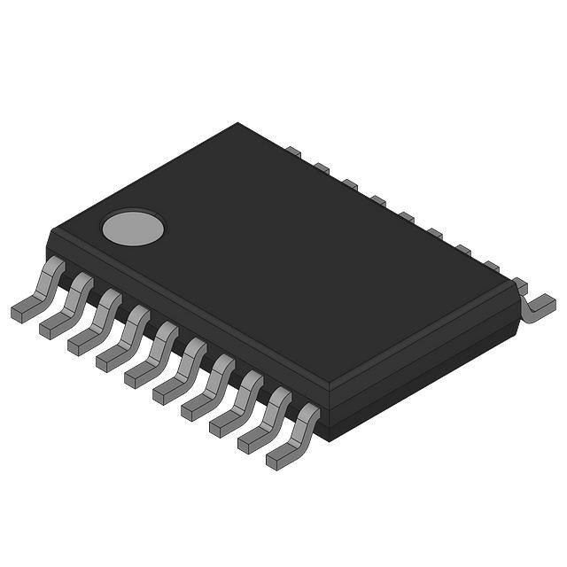
PACKAGE:
20-Pin eTSSOP with Exposed Thermal Pad (suffix LP)
Integrated diagnostics provide indication of undervoltage,
overtemperature, and power bridge faults and can protect the
power switches under most short-circuit conditions. Faults
are indicated by a single open-drain output than can be used
to pull the PWM input low.
The A4962 is provided in a small, thermally enhanced 20-pin
TSSOP with exposed thermal pad.
Not to scale
VBAT
VBAT
PWM
PWM
P
P
FAULTn
ECU
COMMS
P
FAULTn
P
P
P
3-Phase
Motor
A4962
MCU
ECU
N
N
N
N
SPD
3-Phase
Motor
A4962
N
N
Typical Application – Functional Block Diagrams
A4962-DS, Rev. 4
MCO-0000336
January 20, 2020
�A4962
Sensorless BLDC Controller
SELECTION GUIDE
Part Number
Packing
Package
A4962KLPTR-T
4000 pieces per reel
6.5 mm × 4.4 mm, 1.2 mm nominal height
20-pin TSSOP with exposed thermal pad
Table of Contents
Features and Benefits 1
Description 1
Applications 1
Package 1
Typical Application Diagrams 1
Selection Guide 2
Absolute Maximum Ratings 3
Thermal Characteristics 3
Pinout Diagram and Terminal List Table 4
Functional Block Diagram 5
Electrical Characteristics 6
Timing Diagrams 9
Closed-Loop Control Diagrams 11
Functional Description 12
Input and Output Terminal Functions 12
Motor Drive System 13
Motor Control 16
Power Supplies 21
Gate Drive and Bridge PWM 21
Current Limit 24
Diagnostics 27
FAULTn Output 27
Serial Diagnostic Output 27
Fault Action 27
Fault Masks 29
Chip-Level Diagnostics 29
Loss of Synchronization 30
Serial Interface 32
Serial Registers Definition 32
Configuration and Control Registers 33
Diagnostic Register 34
Serial Register Reference 35
Input/Output Structures 40
Package Outline Drawing 41
Allegro MicroSystems
955 Perimeter Road
Manchester, NH 03103-3353 U.S.A.
www.allegromicro.com
2
�A4962
Sensorless BLDC Controller
SPECIFICATIONS
ABSOLUTE MAXIMUM RATINGS*
Characteristic
Symbol
Supply Voltage
Notes
VBB
Rating
Unit
–0.3 to 50
V
Battery-Compliant Inputs
PWM
–0.3 to 50
V
Battery-Compliant Outputs
FAULTn, SPD
–0.3 to 50
V
Logic Inputs
STRn, SCK, SDI
–0.3 to 6.5
V
Logic Outputs
SDO
–0.3 to 6.5
V
VBB – 18 to
VBB + 0.3
V
Pins GHA, GHB, GHC
Pins SA, SB, SC
Pins GLA, GLB, GLC
Sense Amplifier Inputs
VCSI
Ambient Operating Temperature Range
Maximum Continuous Junction Temperature
Storage Temperature Range
CSP, CSM
–4 to 51
V
–0.3 to 18
V
–4 to 6.5
V
TA
–40 to 150
°C
TJ(max)
165
°C
Tstg
–55 to 150
°C
*With respect to GND
THERMAL CHARACTERISTICS: May require derating at maximum conditions; see application information
Characteristic
Package Thermal Resistance
Symbol
RθJA
Test Conditions*
Value
Unit
4-layer PCB based on JEDEC standard
23*
°C/W
2-layer PCB with 3 in.2 copper each side
44*
°C/W
2*
°C/W
RθJT
*Additional thermal information available on the Allegro website.
Allegro MicroSystems
955 Perimeter Road
Manchester, NH 03103-3353 U.S.A.
www.allegromicro.com
3
�A4962
Sensorless BLDC Controller
PINOUT DIAGRAM AND TERMINAL LIST TABLE
VBB
1
20
SA
FAULTn
2
19
SB
SPD
3
18
SC
PWM
4
17
GHA
SDO
5
16
GHB
PAD
SCK
6
15
GHC
STRn
7
14
GLA
SDI
8
13
GLB
GND
9
12
GLC
CSM
10
11
CSP
Package LP, 20-Pin eTSSOP with Exposed Thermal Pad
Terminal List
Name
Number
CSM
10
Sense amp. negative input
Function
Name
Number
SA
20
Function
CSP
11
Sense amp. positive input
SB
19
Phase B motor phase
FAULTn
2
Fault output open drain
SC
18
Phase C motor phase
Phase A motor phase
GHA
17
Phase A HS FET gate drive
SCK
6
Serial clock
GHB
16
Phase B HS FET gate drive
SDI
8
Serial data input
GHC
15
Phase C HS FET gate drive
SDO
5
Serial data output
GLA
14
Phase A LS FET gate drive
SPD
3
Speed output
GLB
13
Phase B LS FET gate drive
STRn
7
Serial strobe (chip select) input
GLA
12
Phase C LS FET gate drive
VBB
1
Main supply
GND
9
Ground
Pad
–
Connect to ground
PWM
4
PWM input, pulled low for fault
Allegro MicroSystems
955 Perimeter Road
Manchester, NH 03103-3353 U.S.A.
www.allegromicro.com
4
�A4962
STRn
SDI
SDO
SCK
Sensorless BLDC Controller
Battery +
Diagnostics &
Protection
Serial Interface
DAC
FAULTn
PWM
PWM
Detect
Start Sequence
& Run Control
VBB
Logic
Supply
Regulator
VREF
Ref
VRI
Dead
Time
Phase A shown
(repeated for B & C)
VBB
GHA
High-Side
Drive
Speed
Control
Phase B
GND
SA
Motor
State
Seq
Gate
Bridge
Drive
Control
Control
x3
VBB
Phase C
GLA
Low-Side
Drive
SPD
GND
Position
Estimator
Blank
Time
+
+
Zero X Detect
–
–
CSP
CSM
VRI
GND
Functional Block Diagram
Allegro MicroSystems
955 Perimeter Road
Manchester, NH 03103-3353 U.S.A.
www.allegromicro.com
5
�A4962
Sensorless BLDC Controller
ELECTRICAL CHARACTERISTICS: Valid at TA= 25°C, VBB = 4.2 to 28 V, unless noted otherwise
Characteristics
Symbol
Test Conditions
Min.
Typ.
Max.
Unit
Operating; outputs active
4.2
–
50
V
Operating; outputs disabled
4.0
–
50
V
0
–
50
V
SUPPLY AND REFERENCE
VBB Functional Operating
Range [1]
VBB
No unsafe states
VBB Quiescent Current
IBBQ
System Clock Period
tOSC
PWM = inactive, VBB = 12 V
–
12
18
mA
47.5
50
52.5
ns
–
200
–
ns
GATE OUTPUT DRIVE
Turn-On Time
tr
CLOAD = 500 pF, 20% to 80%, VBB = 12 V
Turn-Off Time
tf
CLOAD = 500 pF, 20% to 80%, VBB = 12 V
–
200
–
ns
TJ = 25°C, IGHx = –40 mA [2]
12
17
26
Ω
TJ = 150°C, IGHx = –40
20
30
44
Ω
–
300
–
mA
GHx Pull-Up On Resistance
GHx Pull-Up Current Limit
GHx Pull-Down On Resistance
GHx Pull-Down Current Limit
GHx Output Voltage High (Off)
RGHUP
mA [2]
IGHLIMUP
RGHDN
TJ = 25°C, IGHx = 40 mA, VBB = 10 V
18
24
32
Ω
TJ = 150°C, IGHx = 40 mA, VBB = 10 V
30
40
50
Ω
–
100
–
mA
IGHLIMDN
VGHH
–10 µA < IGH < 10 µA
IGH = 10 mA, VBB = 14.5 V
GHx Output Voltage Low (Active)
GLx Pull-Up On Resistance
GLx Pull-Up Current Limit
GLx Pull-Down On Resistance
GLx Pull-Down Current Limit
VGHL
RGLUP
–10 µA < IGH < 10 µA, VBB ≥ 14.1 V
–10 µA < IGH < 10 µA, 9.6 ≤ VBB < 14.1 V
GLx Output Voltage Low (Off)
VGLL
V
4.4
V
VBB – 14.1
–
VBB – 10.7
V
0
–
VBB – 9.4
V
0
–
0.2
V
17
24
31
Ω
TJ = 150°C, IGLx = –40 mA [2], VBB = 10 V
25
35
45
Ω
–
140
–
mA
TJ = 25°C, IGLx = 40 mA
13
20
25
Ω
TJ = 150°C, IGLx = 40 mA
25
35
45
Ω
–
160
–
mA
IGLLIMDN
VGLH
–
–
TJ = 25°C, IGLx = –40 mA [2], VBB = 10 V
–10 µA < IGL < 10 µA, VBB < 8.6 V
GLx Output Voltage High (Active)
–
0.9
–10 µA < IGH < 10 µA, VBB < 9.6 V
IGLLIMUP
RGLDN
VBB – 0.2
VBB – 0.2
–
VBB
V
–10 µA < IGL < 10 µA, 8.6 ≤ VBB < 13.7 V
8.4
–
VBB
V
–10 µA < IGL < 10 µA, VBB ≥ 13.7 V
11.2
–
13.7
V
IGL = –10 mA, VBB = 14.5 V
10
–
13
V
–10 µA < IGL < 10 µA
–
–
0.2
V
GHx Passive Pull-Down
RGHPD
VBB = 0 V, VGH > –0.1 V
–
500
–
kΩ
GLx Passive Pull-Down
RGLPD
VBB = 0 V, VGL < 0.1 V
–
500
–
kΩ
–
300
–
ns
–
300
–
ns
0.9
1.0
1.1
µs
Turn-Off Propagation Delay [3]
tP(off)
Input Change to unloaded Gate output change;
Direct mode
Turn-On Propagation Delay [3]
tP(on)
Input Change to unloaded Gate output change;
Direct mode
Dead Time (Turn-Off to Turn-On
Delay) [3]
tDEAD
Default power-up value
Continued on next page...
Allegro MicroSystems
955 Perimeter Road
Manchester, NH 03103-3353 U.S.A.
www.allegromicro.com
6
�A4962
Sensorless BLDC Controller
ELECTRICAL CHARACTERISTICS (continued): Valid at TA= 25°C, VBB = 4.2 to 28 V, unless noted otherwise
Characteristics
Symbol
Test Conditions
Min.
Typ.
Max.
Unit
VIL
–
–
0.8
V
Input High Voltage (except PWM)
VIH
2.0
–
–
V
Input High Voltage (PWM)
VIH
2.1
–
–
V
LOGIC INPUTS AND OUTPUTS
Input Low Voltage
Input Hysteresis
VIhys
150
550
–
mV
Input Pull-Down Resistor (PWM, SDI,
SCK)
RPD
30
50
70
kΩ
Input Pull-Up Resistor (STRn)
RPU
30
50
70
kΩ
Output Low Voltage (SDO)
VOL
IOL = 1 mA
–
0.2
0.4
V
Output High Voltage (SDO)
VOH
IOL = 1 mA [2]
2.4
3.0
–
V
IO
0 V < VO < 5.5 V, STRn = 1
–1
–
1
µA
VOL
IOL = 4 mA, FAULTn active
–
0.2
0.4
V
0 V < VO < 15 V, FAULTn active
–
10
17
mA
Output
Leakage [2]
(SDO)
Output Low Voltage (FAULTn, SPD)
Output Current Limit (FAULTn, SPD)
Output Leakage [2] (FAULTn, SPD)
IOLIM
IO
15 V ≤ VO < 50 V, FAULTn active
–
–
2
mA
0 V < VO < 12 V, FAULTn inactive
–1
–
1
µA
12 V ≤ VO < 50 V, FAULTn inactive
–
–
1.7
mA
LOGIC I/O – TIMING PARAMETERS
PWM Duty Detect Frequency Range
fPWD
5
–
1000
Hz
PWM Brake Time
tBRK
500
–
–
µs
SERIAL INTERFACE – TIMING PARAMETERS
Clock High Time
tSCKH
A in Figure 1
50
–
–
ns
Clock Low Time
tSCKL
B in Figure 1
50
–
–
ns
Strobe Lead Time
tSTLD
C in Figure 1
30
–
–
ns
Strobe Lag Time
tSTLG
D in Figure 1
30
–
–
ns
Strobe High Time
tSTRH
E in Figure 1
300
–
–
ns
Data Out Enable Time
tSDOE
F in Figure 1
–
–
40
ns
Data Out Disable Time
tSDOD
G in Figure 1
–
–
30
ns
Data Out Valid Time from Clock Falling
tSDOV
H in Figure 1
–
–
40
ns
Data Out Hold Time from Clock Falling
tSDOH
I in Figure 1
5
–
–
ns
Data In Setup Time to Clock Rising
tSDIS
J in Figure 1
15
–
–
ns
Data In Hold Time from Clock Rising
tSDIH
K in Figure 1
10
–
–
ns
MOTOR STARTUP PARAMETERS
Hold Duty Cycle
DH
Default power-up value
35.5
37.5
39.5
%
tHOLD
Default power-up value
15.2
16
16.8
ms
Start Speed
fST
Default power-up value
7.6
8
8.4
Hz
Start Duty Cycle
DST
Default power-up value
47.5
50
52.5
%
Hold Time
Continued on next page...
Allegro MicroSystems
955 Perimeter Road
Manchester, NH 03103-3353 U.S.A.
www.allegromicro.com
7
�A4962
Sensorless BLDC Controller
ELECTRICAL CHARACTERISTICS (continued): Valid at TA= 25°C, VBB = 4.2 to 28 V, unless noted otherwise
Characteristics
Symbol
Test Conditions
Min.
Typ.
Max.
Unit
MOTOR RUN PARAMETERS
Phase Advance (in Electrical Degrees)
θADV
Default power-up value
14
15
16
°
Position Control Proportional Gain
KCP
Default power-up value
–
1
–
–
Position Control Integral Gain
KCI
Default power-up value
–
1
–
–
Speed Control Proportional Gain
KSP
Default power-up value
–
1
–
–
Speed Control Integral Gain
KSI
Default power-up value
–
1
–
–
fMX
Default power-up value
3112.9
3276.7
3440.5
Hz
–5
–
5
%
12.5
–
200
mV
–
200
–
mV
Maximum Control Speed
Speed Error
EfCCMX
CURRENT LIMITING
Current Limit Threshold Voltage
Range
VILIM
VILIM = VCSP – VCSM
Current Limit Threshold Voltage
VILIM
Default power-up value
Current Limit Threshold Voltage
Error [7]
EILIM
VILIM = 200 mV
–5%
–
5%
%FS
Fixed Off-Time
tPW
Default power-up value
47.9
50.4
52.9
µs
Blank Time
tBL
Default power-up value
3.04
3.2
3.36
µs
PROTECTION
VBB Undervoltage Lockout
VBB POR Voltage
VBB POR Voltage Hysteresis
VDS Threshold
VBBON
VBB rising
4.2
4.4
4.6
V
VBBOFF
VBB falling
3.8
4.0
4.2
V
VBBR
VBB falling
–
3.2
3.5
V
–
100
–
mV
VBBRHys
VDST
Default power-up value
1325
1550
1705
mV
VBB ≥ 7 V
–
–
1705
mV
–
–
1000
mV
VDS Threshold Max, High Side
VDST
6 V ≤ VBB < 7 V
5.5 V ≤ VBB < 6 V
–
–
400
mV
VDS Threshold Max, Low Side
VDST
VBB ≥ 4.2 V
–
–
1705
mV
VDS Threshold Offset [4][5]
VDSTO
Temperature Warning Threshold
TJWH
Temperature Warning Hysteresis
TJWHhys
VDST ≥ 1 V
–
±100
–
mV
VDST ≤ 1 V
–150
±50
150
mV
Temperature increasing
125
135
150
°C
–
15
–
°C
Overtemperature Threshold
TJF
Temperature increasing
170
175
180
°C
Overtemperature Hysteresis
TJHyst
Recovery = TJF – TJHyst
–
15
–
°C
[1]
[2]
[3]
[4]
[5]
[6]
[7]
Function is correct but parameters are not guaranteed above or below the general limits (6-28 V).
For input and output current specifications, negative current is defined as coming out of (sourcing) the specified device terminal.
See Figure 2 for gate drive output timing.
As VSX decreases, high-side fault occurs if (VBAT – VSX) > (VDST + VDSTO).
As VSX increases, low-side fault occurs if (VSX) > (VDST + VDSTO).
See Figures 4 and 5 for VDS monitor timing.
Current limit threshold voltage error is the difference between the target threshold voltage and the actual threshold voltage, referred to maximum full-scale (100%) current: EILIM = 100 × (VILIMActual – VILIM) / 200% (VILIM in mV).
Allegro MicroSystems
955 Perimeter Road
Manchester, NH 03103-3353 U.S.A.
www.allegromicro.com
8
�A4962
Sensorless BLDC Controller
STRn
A
C
E
D
B
SCK
J
SDI
K
D15
X
X
F
SDO
X
D14
X
D0
X
G
I
Z
D14’
D15’
Z
D0’
H
X = don’t care; Z = high impedance (tri-state)
Figure 1: Serial Interface Timing
PWM
tDEAD
tP(off)
GHX
GLX
tP(off)
tDEAD
Figure 2: Gate Drive Timing
VBB (V)
2
14
0
12
-2
4
6
8
10
12
VGS(HS) Spec Max
VGS(HS) Typical
VGS(HS) Spec Min
14
16
18
20
VBB
VGS(HS)
-4
VGS(HS) (V)
VGS(LS) (V)
10
8
VBB
6
GHA
GHA
-6
GLA
-8
-10
4
GLA
VGS(LS) Spec Max
VGS(LS) Typical
VGS(LS) Spec Min
2
-12
VGS(LS)
-14
0
2
4
6
8
10
12
14
16
18
20
VBB (V)
Figure 3: Typical Low-Side Gate Drive vs. VBB
Figure 4: Typical High-Side Gate Drive vs. VBB
Allegro MicroSystems
955 Perimeter Road
Manchester, NH 03103-3353 U.S.A.
www.allegromicro.com
9
�A4962
Sensorless BLDC Controller
VDS Fault Monitor Timing Diagrams
Bridge
PWM
tDEAD
tP(off)
GHX
tBL
High-side VDS monitor active
HS monitor disabled
High-side VDS monitor disabled
tP(off)
tDEAD
GLX
tBL
Low-side VDS monitor disabled
Low-side VDS monitor active
disabled
Figure 5: VDS Fault Monitor – Blank Mode Timing (VDQ = 1)
MOSFET turn on
No fault present
MOSFET turn on
Fault present
MOSFET on
Transient disturbance
Fault present
MOSFET on
Fault occurs
Gate
Active
VDS
tVDQ
tVDQ
Fault Bit
Figure 6: VDS Fault Monitor – Blank Mode Timing (VDQ = 1)
MOSFET turn on
No fault present
MOSFET turn on
Fault present
MOSFET on
Transient disturbance
No fault present
MOSFET on
Fault occurs
Gate
Active
VDS
tVDQ
tVDQ
tVDQ
tVDQ
Fault Bit
Figure 7: VDS Fault Monitor – Debounce Mode Timing (VDQ = 0)
Allegro MicroSystems
955 Perimeter Road
Manchester, NH 03103-3353 U.S.A.
www.allegromicro.com
10
�A4962
Sensorless BLDC Controller
Closed-Loop Control Diagrams
VBAT
PWM
Communication Bus
P
FAULTn
P
P
ECU
3-Phase
Motor
A4962
MCU
N
N
SPD
N
Figure 8: Local Closed-Loop Control with High Level ECU Communications
VBAT
Low Frequency PWM Speed or Current Demand
PWM
P
FAULTn
P
P
3-Phase
Motor
A4962
ECU
N
Low Frequency SpeedFeedback
N
SPD
N
Figure 9: Remote Closed-Loop Control
VBAT
Low Frequency PWM Speed or Current Demand
PWM
P
FAULTn
P
P
3-Phase
Motor
A4962
ECU
N
SPD
N
N
Figure 10: Remote Single-Wire Command with Integrated Closed-Loop Control
Allegro MicroSystems
955 Perimeter Road
Manchester, NH 03103-3353 U.S.A.
www.allegromicro.com
11
�A4962
Sensorless BLDC Controller
FUNCTIONAL DESCRIPTION
The A4962 is a three-phase, sensorless, brushless DC (BLDC)
motor controller for use with external complementary P-channel
and N-channel power MOSFETs and is specifically designed for
automotive applications. The motor is driven using block commutation (trapezoidal drive), where phase commutation is determined by a proprietary, motor back-emf (bemf) sensing technique. The motor bemf is sensed to determine the rotor position
without the need for independent position sensors. An integrated
sensorless startup scheme allows a wide range of motor and load
combinations.
Motor current is provided by six external power MOSFETs
arranged as a three-phase bridge with three N-channel lowside MOSFETs and three P-channel high-side MOSFETS. The
A4962 provides six high current gate drives, three high-side and
three low-side, capable of driving a wide range of MOSFETs.
The maximum MOSFET drive voltage is internally limited
under all supply conditions to protect the MOSFET from excessive gate-source voltage without the need for an external clamp
circuit. The minimum MOSFET drive voltage is determined by
the supply voltage allowing operation at very low voltage by
using logic-level MOSFETs.
Three basic operational modes are available: open-loop speed
(voltage) control, closed-loop torque (current) control, and
closed-loop speed control. Operating mode and control parameters can be altered through an SPI-compatible serial interface.
Motor operation is controlled by a single, low-frequency PWM
input that determines the motor operating state and provides
proportional input for the selected operating mode.
Input and Output Terminal Functions
VBB: Main power supply for internal regulators and charge
pump. The main power supply should be connected to VBB
through a reverse voltage protection circuit and should be
decoupled with ceramic capacitors connected close to the supply
and ground terminals.
GND: Analog reference, Digital and power ground. Connect to
supply ground—see layout recommendations.
GHA, GHB, GHC: High-side, gate drive outputs for external
P-channel MOSFETs.
SA, SB, SC: Motor phase connections. These terminals sense
the voltages switched across the load.
GLA, GLB, GLC: Low-side, gate drive outputs for external
N-channel MOSFETs.
CSP, CSM: Differential current sense amplifier inputs. Connect
directly to each end of the sense resistor using separate PCB
traces.
PWM: Programmable PWM input to control the motor operating mode and the proportional duty cycle input for the selected
control mode. Can be shorted to ground or VBB without damage.
SPD: Open-drain speed output indicator. Output frequency is
programmable. It can be the commutation frequency (TACHO)
or the electrical cycle frequency (FG). Can be shorted to ground
or VBB without damage.
Startup (inrush) current and peak motor current are limited by
an integrated fixed off-time PWM current limiter. The maximum
current limit is set by a single external sense resistor, and the
active current limit can be modified through the serial interface.
FAULTn: Open-drain active-low fault indicator. Can be connected to PWM input to provide single wire interface to a controlling ECU. Can be shorted to ground or VBB without damage.
Integrated diagnostics provide indication of undervoltage,
overtemperature, and power bridge faults and can be configured
to protect the power FETs under most short-circuit conditions.
A single FAULT flag is provided, and detailed diagnostics are
available through the serial interface.
SDO: Serial data output. High impedance when STRn is high.
Outputs bit 15 of the diagnostic register, the fault flag, as soon as
STRn goes low.
Specific functions are described more fully in following sections.
SDI: Serial data input. 16-bit serial word input msb first.
SCK: Serial clock. Data is latched in from SDI on the rising
edge of CLK. There must be 16-rising edges per write and SCK
must be held high when STRn changes.
STRn: Serial data strobe and serial access enable. When STRn
is high, any activity on SCK or SDI is ignored and SDO is high
impedance, allowing multiple SDI slaves to have common SDI,
SCK, and SDO connections.
Allegro MicroSystems
955 Perimeter Road
Manchester, NH 03103-3353 U.S.A.
www.allegromicro.com
12
�A4962
Sensorless BLDC Controller
Motor Drive System
The motor drive system consists of three half-bridge gate drive
outputs, each driving one leg of an external 3-phase MOSFET
power bridge. The state of the gate drive outputs is determined
by a state sequencer with six possible states. These states are
shown in Table 1 and change in a set sequence. The effect of
these states on the motor phase voltage is illustrated in Figure
11. This sequence creates a moving magnetic field in the poles of
the stator, against which the permanent magnets in the rotor can
react to produce torque at the motor output shaft.
Seq
1
2
3
4
5
6
1
2
3
4
6
5
SA
SB
The point at which the state of the gate outputs change is defined
as the commutation point and must occur each time the magnetic
poles of the rotor reach a specific point in relation to the poles of
the stator. This point is determined by a closed-loop commutation controller consisting of a position estimator and commutation timer. This controller uses the output of a complete selfcontained bemf sensing scheme to determine the actual position
of the motor and adjust the estimated position and commutation
frequency to synchronize with the rotor poles in the motor.
SC
TACHO
FG
Figure 11: Motor Phase State Sequence
In the A4962, motor speed is always defined as the frequency
of the electrical cycle, fS. This is the same frequency as the FG
signal, if selected, on the SPD output.
The motor speed can be determined by monitoring the SPD
output. There are two options for the signal available at the
SPD terminal selected via the serial interface. The default is a
signal, defined as FG, at the frequency of the complete electrical
cycle (the 6-state sequence in Table 1). FG goes high on entering state 1 and goes low on entering state 4. The alternative is
a square wave signal, defined as TACHO, at the commutation
frequency with the falling edge synchronized to the commutation
point. FG and TACHO are shown in Figure 11.
The actual mechanical speed of the motor, ω, will depend on the
number of pole pairs, NPP, and is determined by:
�=
60 × fs
NPP
where fS is in Hz and ω is in rpm (mechanical revolutions per
minute).
Table 1: Control and Phase Sequence
Control Bits
RUN
BRK
1
0
DIR=1
DIR0
State
1
Motor Phase
Gate Drive Outputs
SA
SB
SC
GHA
GLA
GHB
GLB
GHC
GLC
HI
Z
LO
ON
OFF
OFF
OFF
OFF
ON
1
0
2
Z
HI
LO
OFF
OFF
ON
OFF
OFF
ON
1
0
3
LO
HI
Z
OFF
ON
ON
OFF
OFF
OFF
1
0
4
LO
Z
HI
OFF
ON
OFF
OFF
ON
OFF
1
0
5
Z
LO
HI
OFF
OFF
OFF
ON
ON
OFF
1
0
6
HI
LO
Z
ON
OFF
OFF
ON
OFF
OFF
Mode
Run
0
x
x
x
x
Z
Z
Z
OFF
OFF
OFF
OFF
OFF
OFF
Coast
1
1
x
x
x
LO
LO
LO
OFF
ON
OFF
ON
OFF
ON
Brake
x ≡ don’t care, HI ≡ high-side FET active, LO ≡ low-side FET active, Z ≡ high impedance, both FETs off
ON ≡ high-side output (GHx) low, low-side output (GLx) high
OFF ≡ high-side output (GHx) high, low-side output (GLx) low
Allegro MicroSystems
955 Perimeter Road
Manchester, NH 03103-3353 U.S.A.
www.allegromicro.com
13
�A4962
Sensorless BLDC Controller
Rotor Position Sensing Using Motor bemf
A key element of the controller is the back-emf zero crossing detector. Determining the rotor position using direct bemf
sensing relies on the accurate comparison of the voltage on the
undriven (tri-state) motor phase (indicated by Z in Table 1) to
the voltage at the center tap of the motor, approximated using an
internally generated reference voltage. The bemf zero crossing—the point where the voltage of the undriven motor winding
crosses the reference voltage—occurs when a pole of the rotor is
in alignment with a pole of the stator and is used as a positional
reference for the commutation controller.
The internally generated zero crossing reference voltage follows
the bridge drive voltage levels to allow bemf crossing detection
during both PWM-on and PWM-off states. The comparator adds
hysteresis to the reference voltage in order to reduce the effect
of low-level noise on the comparison. The effects of large signal
noise, such as switching transients, are removed by digital filtering.
When the motor is running at a constant speed, with no phase
advance, this zero crossing should occur approximately halfway
through one commutation period. The commutation controller
compares the expected zero crossing point to the detected zero
crossing point and adjusts the phase and frequency of the position estimator and commutation timer to minimize the difference
between the expected and actual crossing points over a number
of commutation periods.
The controller also allows the commutated magnetic field of
the stator to be out of phase with the rotor. The expected zero
crossing point is adjusted to be later in the commutation period,
and the controller modifies the commutation timing to minimize
the difference between the estimated and measured bemf zerocrossing points. This is known as phase advance, and the amount
of phase advance in electrical degrees is set (up to 28°) by the
contents of the PA[3:0] variable.
In any electric motor, a force is produced by the interaction of
rotor magnetic poles and stator magnetic field. The motor and
the commutation system are designed such that a portion of
this force is tangential to the rotor and will produce a rotational
torque. Applying phase advance will have the effect of changing the direction of force vector relative to the rotor and will
increase the tangential component of the force. This will increase
the effectiveness of the torque produced by the stator field and
permit a higher motor speed than for no phase advance at the
same input demand.
The controller uses proportional and integral feedback (PI
control) to provide a fast response with good long-term accuracy. The amount of proportional and integral feedback can be
adjusted independently by setting the CP[3:0] and CI[3:0] variables respectively, through the serial interface. This allows the
dynamic response to be tuned to different system conditions if
required; however, the default values for CP and CI will achieve
optimum results in most applications.
The control method used is tolerant to missing bemf zero crossing detections and will simply change the speed of the applied
commutation sequence by an amount determined by the proportional gain of the control loop. This results in a much more
stable system that does not lose synchronization due to impulse
perturbations in the motor load torque. It also means that real
loss of synchronization cannot be determined by missing bemf
zero crossing detection and has to be determined in a different
way.
In the extreme case, when a motor stalls due to excessive load
on the output, there will be no bemf zero crossing detection,
and the frequency of the commutation sequence will be reduced
each commutation point to try and regain synchronization. If the
resulting speed reduces below the low speed threshold, then the
controller will enter the loss of synchronization state and either
stop or attempt to restart the motor. The low speed threshold will
be 25% of the start speed set by the value of the SS[3:0] variable.
In some cases, rather than a complete stall, it is also possible
for the motor to vibrate at a whole fraction (subharmonic) of
the commutation frequency produced by the controller. In this
case, the controller will still detect the bemf zero crossing, but
at a rate much higher than the motor is capable of running. If the
resulting speed increases above the overspeed threshold, then the
controller will enter the loss of synchronization state and either
stop or attempt to restart the motor. The overspeed threshold is
determined by the product of the maximum limit ratio and the
maximum speed. The maximum limit ratio is set by the value of
the SH[1:0] variable, and the maximum speed is by set the value
of the SMX[2:0] variable.
The maximum speed, defined by SMX, determines the motor
speed for 100% input when operating in the closed-loop speed
control mode. However, it must still be set to a suitable level to
provide an appropriate overspeed threshold for all other operating modes.
Allegro MicroSystems
955 Perimeter Road
Manchester, NH 03103-3353 U.S.A.
www.allegromicro.com
14
�A4962
Sensorless BLDC Controller
Startup
To correctly detect the zero crossing, the changing motor bemf
on any phase must be detectable when that phase is not being
driven. When the motor is running at a relatively constant speed,
this is ensured by the commutation scheme used. However, during startup, the motor must be accelerated from rest in such a
way that the bemf zero crossing can be detected. Initially, as the
motor is started, there is no rotor position information from the
bemf sensor circuits, and the motor must be driven using forced
commutation.
mode used during running will not be able to maintain control
of the motor current during the PWM off-time, and the current
may rise uncontrollably. To overcome this effect, the A4962 uses
a mixed decay mode PWM during startup to keep the current
under control. Mixed decay is where the bridge is first switched
into fast decay mode then into slow decay after a portion of the
PWM period. This applies a reverse voltage to the motor phase
winding and counteracts the effect of the out-of-phase bemf
voltage.
To ensure that the motor startup and sensorless bemf capture
is consistent, the start sequencer always forces the motor to a
known hold position and for a programmable hold time by driving phase C low and applying a programmable duty cycle PWM
signal to phase A. The hold time is defined by the contents of the
HT[3:0] variable and the hold duty cycle by the contents of the
HD[3:0] variable.
The portion of the PWM period during which fast decay is used
is called percent fast decay (PFD). Two values of PFD—12.5%
or 25%—can be selected by the PFD variable in configuration
register 1. Mixed decay is applied automatically for the first
sixteen full electrical cycles (96 commutation periods).
Following the hold time, the motor phases are commutated to
the next state to force the motor to start in the required direction,
and the PWM duty cycle is changed to the startup duty cycle set
by the contents of the SD[3:0] variable. For the forwards direction when DIR = 0, phase C will be held low, and the startup
duty cycle is applied to phase B. For the reverse direction when
DIR = 1, phase B will be held low, and the startup duty cycle is
applied to phase A. The duration of the first commutation period
is determined by the start speed set by the value of the SS[3:0]
variable. This value is also used as the starting speed for the
closed-loop commutation controller and for the speed controller
if selected.
At the end of the second commutation period, control is
passed to the closed-loop commutation controller, and the start
sequencer is reset. The SPD terminal will immediately output
FG or TACHO as selected by the SPO variable.
During the start sequence, it is possible for the motor to be
rotating out of synchronization with the commutated field,
as sequenced by the A4962. In some cases, it is possible for
the motor bemf produce a voltage that reinforces, rather than
opposes, the supply voltage. If this occurs, then the slow decay
Following the start sequence, the commutation controller is
expected to attain synchronization with the motor and stabilize
at a running frequency to match the control input demand. If
synchronization is not achieved, the commutation controller will
either reduce the resulting motor frequency below the low-speed
limit or increase it above the overspeed limit. If this happens,
the A4962 will indicate a loss of synchronization condition by
repeatedly pulling the FAULTn output active low for three PWM
periods and inactive for three periods.
If a loss of synchronization occurs, the RUN and RSC bits are
set to 1, and the PWM signal applied to the PWM input terminal is not 0% (or is not less than 25% for closed-loop speed
control mode) then the FAULTn output will go active low for
three PWM periods, inactive for three periods, then repeat
this sequence before the start sequencer is reset and the start
sequence initiated as shown in Figure 4. This cycle will continue
until stopped by holding the PWM terminal in the inactive state
or setting either RUN bit or the RSC bit to 0.
If a loss of synchronization occurs and RSC = 0, the FAULTn
output will continue to indicate loss of synchronization until the
PWM signal applied to the PWM input terminal is 0% (or


 工商网监
湘ICP备2023018690号
工商网监
湘ICP备2023018690号
