A5984
DMOS Microstepping Driver with Translator
and Overcurrent Protection
FEATURES AND BENEFITS
•
•
•
•
•
•
•
•
•
•
•
•
•
•
•
•
•
DESCRIPTION
Drop-in replacement for A4984
Proprietary Adaptive Percent Fast Decay option
Low RDS(on) outputs
Single supply
Microstepping up to 32 microsteps per full step
Full torque step modes
Short-to-ground protection
Shorted load protection
Short-to-battery protection
Fault output
Low current Sleep mode, < 10 µA
No smoke no fire (NSNF) compliance (ET package)
Thin profile QFN and TSSOP packages
Thermal shutdown circuitry
Synchronous rectification for low power dissipation
Internal UVLO
Crossover-current protection
APPLICATIONS
• Video Security Cameras
• Printers
• Scanners
• Robotics
• ATM
• POS
The A5984 is a complete microstepping motor driver with
built-in translator for easy operation. It is designed to operate
bipolar stepper motors from full-step up to 1/32 step modes.
Step modes are selectable by MSx logic inputs. It has an output
drive capacity of up to 40 V and ±2 A.
A5984 introduces a proprietary Adaptive Percent Fast Decay
(APFD) algorithm to optimize the current waveform over a
wide range of stepper speeds and stepper motor characteristics.
APFD adjusts on-the-fly the amount of fast decay during a
PWM cycle to keep current ripple at a low level over the
various operating conditions. This adaptive feature improves
performance of the system resulting in reduced audible motor
noise, reduced vibration, and increased step accuracy.
The translator is the key to the easy implementation of the
A5984. Simply inputting one pulse on the STEP input drives
the motor one microstep. There are no phase sequence tables,
high frequency control lines, or complex interfaces to program.
The A5984 interface is an ideal fit for applications where a
complex microprocessor is unavailable or is overburdened.
The ET package meets customer requirements for no smoke
no fire (NSNF) designs by adding no-connect pins between
critical output, sense, and supply pins. So, in the case of a
pin-to-adjacent-pin short, the device does not cause smoke
or fire. Additionally, the device does not cause smoke or fire
when any pin is shorted to ground or left open.
Continued on the next page…
5V
0.1 µF
0.1 µF
5 kΩ
SLEEP
ROSC
CP1
CP2
VCP
VBB2
STEP
MS1
Microcontroller or
Controller Logic
MS2
MS3
VBB1
OUT1A
A5984
OUT1B
SENSE1
DIR
ENABLE
RESET
5V
OUT2A
VREF
OUT2B
5 kΩ
nFAULT
SENSE2
GND
PAD
Typical Application Diagram
5984-DS, Rev. 1
100 µF
�DMOS Microstepping Driver with Translator
and Overcurrent Protection
A5984
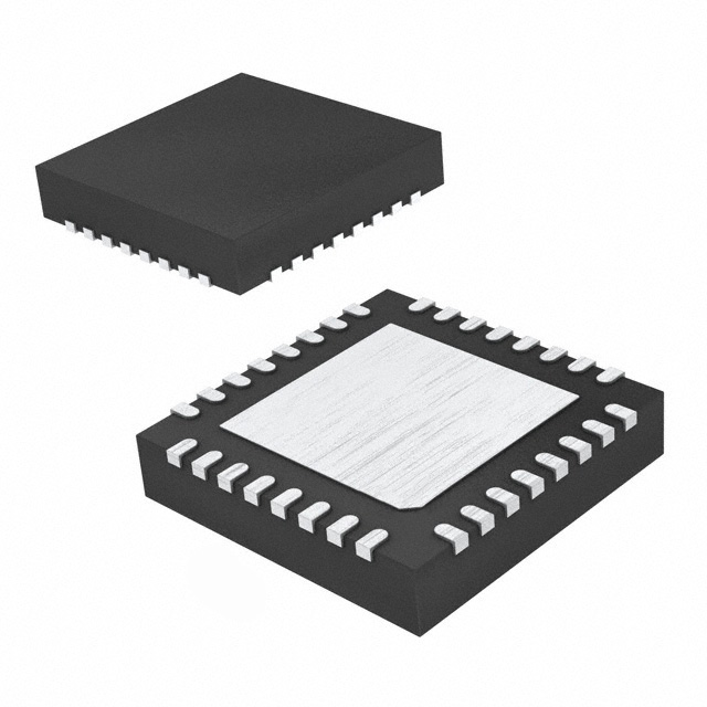
PACKAGES:
DESCRIPTION (continued)
Internal synchronous rectification control circuitry is provided to
improve power dissipation during PWM operation. Internal circuit
protection includes: thermal shutdown with hysteresis, undervoltage
lockout (UVLO), and crossover-current protection. Special power-on
sequencing is not required.
24-contact QFN
with exposed thermal pad
4 mm × 4 mm × 0.75 mm
(ES package)
The A5984 is supplied in three surface mount packages: two QFN
packages, the 4 mm × 4 mm, 0.75 mm nominal overall height ES
package, and the 5 mm × 5 mm × 0.90 mm ET package. The LP
package is a 24‑pin TSSOP. All three packages have exposed pads
for enhanced thermal dissipation, and are lead (Pb) free (suffix –T),
with 100% matte-tin-plated leadframes.
32-contact QFN
with exposed thermal pad
5 mm × 5 mm × 0.90 mm
(ET package)
24-pin TSSOP
with exposed thermal pad
(LP Package)
SPECIFICATIONS
Selection Guide
Part Number
Package
Packing
A5984GESTR-T
24-pin QFN with exposed thermal pad
1500 pieces per 7-in. reel
A5984GETTR-T*
32-pin QFN with exposed thermal pad
1500 pieces per 7-in. reel
A5984GLPTR-T
24-pin TSSOP with exposed thermal pad
4000 pieces per 13-in. reel
* Contact marketing for availability.
Absolute Maximum Ratings
Characteristic
Symbol
Notes
Rating
Units
Load Supply Voltage
VBB
40
V
Output Current
IOUT
±2
A
Logic Input Voltage
VIN
Motor Outputs Voltage
Sense Voltage
Reference Voltage
Operating Ambient Temperature
Maximum Junction
Storage Temperature
VSENSE
VREF
–0.3 to 6
V
–2.0 to VBB + 2 V
V
–0.5 to 0.5
V
5.5
V
–40 to 105
ºC
TJ(max)
150
ºC
Tstg
–55 to 150
ºC
TA
Range G
Allegro MicroSystems, LLC
115 Northeast Cutoff, Box 15036
Worcester, Massachusetts 01615-0036 (508) 853-5000
www.allegromicro.com
2
�A5984
DMOS Microstepping Driver with Translator
and Overcurrent Protection
Table of Contents
Specifications
Functional Block Diagram
Pinout Diagrams and Terminal List Table
Electrical Characteristics
Thermal Characteristics
Logic Interface
Functional Description
2
4
5
6
7
8
9
Device Operation
9
Stepping Current Control
9
100 Percent Torque Operation
9
9
Microstep Select (MSx)
Reset Input (¯R¯ ¯E¯ ¯S¯ ¯E¯ ¯T¯ )
9
Step Input (STEP)
12
Direction Input (DIR)
12
12
Internal PWM Current Control
Blanking 12
12
ROSC
Charge Pump (CP1 and CP2)
12
¯ ¯E¯ )
Enable Input ( ¯E¯ ¯
N¯ ¯
A¯ ¯B¯ ¯L
12
¯ ¯E
¯ ¯E
¯ ¯P
¯ )
13
Sleep Mode ( S¯ ¯L
Synchronous Rectification
13
Protection Functions
Fault Output (nFAULT)
Thermal or Undervoltage Fault Shutdown
Overcurrent Protection
Application Information
13
13
13
13
14
Layout
Pin Circuit Diagrams
Phase Current Diagrams
Full Step (100% Torque)
Half Step (100% Torque)
Sixteenth Step
Thirty-Secondth Step
Full Step (Modified)
Half Step (Modified)
Eighth Step
Quarter Step
Stepping Phase Tables
Full Torque Modes
Common Modes
14
15
16
16
16
17
17
18
18
19
19
20
20
21
Package Outline Drawings
25
Allegro MicroSystems, LLC
115 Northeast Cutoff, Box 15036
Worcester, Massachusetts 01615-0036 (508) 853-5000
www.allegromicro.com
3
�DMOS Microstepping Driver with Translator
and Overcurrent Protection
A5984
0.1 µF
ROSC
Internal
Regulator
CP1
CP2
Charge
Pump
OSC
VCP
0.1 µF
REF
DMOS Full Bridge
DAC
VBB1
OUT1A
OUT1B
PWM Latch
Blanking
Mixed Decay
STEP
DIR
OCP
Gate
Drive
RESET
MS1
100 kΩ
Translator
MS2
SENSE1
DMOS Full Bridge
Control
Logic
100 kΩ
PWM Latch
Blanking
Mixed Decay
100 kΩ
ENABLE
OUT2B
SENSE2
Fault
RS2
DAC
SLEEP
RS1
OUT2A
OCP
MS3
VBB2
5V
VREF
nFAULT
GND
PAD
Functional Block Diagram
Allegro MicroSystems, LLC
115 Northeast Cutoff, Box 15036
Worcester, Massachusetts 01615-0036 (508) 853-5000
www.allegromicro.com
4
�DMOS Microstepping Driver with Translator
and Overcurrent Protection
A5984
OUT2B
1
18 OUT1B
ENABLE
2
17 DIR
GND
3
CP1
4
15 REF
CP2
5
14 STEP
VCP
6
13 MS3
16 GND
PAD
OUT2B
NC
VBB2
NC
ENABLE
GND
CP1
1
2
3
4
5
6
7
CP2
8
25 SENSE1
29 NC
28 NC
27 OUT1A
26 NC
32 SENSE2
31 NC
30 OUT2A
19 VBB1
20 SENSE1
21 OUT1A
22 OUT2A
23 SENSE2
24 VBB2
Pinout Diagrams and Terminal List Table
24
23
22
21
20
19
18
PAD
OUT1B
NC
VBB1
NC
CP1 1
24 GND
CP2 2
23 ENABLE
VCP 3
22 OUT2B
MS2 6
DIR
GND
REF
17 STEP
RESET 7
ROSC 8
SLEEP 9
MS3 16
VCP 9
nFAULT 10
MS1 11
MS2 12
RESET 13
ROSC 14
SLEEP 15
SLEEP 12
ROSC 11
RESET 10
9
MS2
8
MS1
nFAULT 7
20 SENSE2
MS1 5
MS3 10
ES Package Pinouts
21 VBB2
nFAULT 4
STEP 11
REF 12
ET Package Pinouts
PAD
19 OUT2A
18 OUT1A
17 SENSE1
16 VBB1
15 OUT1B
14 DIR
13 GND
LP Package Pinouts
Terminal List Table
Number
Name
CP1
Description
ES
ET*
LP
4
7
1
Charge pump capacitor terminal
CP2
5
8
2
Charge pump capacitor terminal
DIR
17
20
14
Logic input
¯E¯ ¯N¯ ¯
A¯ ¯B¯ ¯L¯ ¯E¯
2
5
23
Logic input
nFAULT
7
10
4
Fault output, active low
GND
3, 16
6, 19
13, 24
MS1
8
11
5
Ground
Logic input
MS2
9
12
6
Logic input
MS3
13
16
10
Logic input
NC
–
2, 4, 21, 23,
26, 28, 29, 31
–
No connection
OUT1A
21
27
18
DMOS Full Bridge 1 Output A
OUT1B
18
24
15
DMOS Full Bridge 1 Output B
OUT2A
22
30
19
DMOS Full Bridge 2 Output A
OUT2B
1
1
22
DMOS Full Bridge 2 Output B
REF
15
18
12
Gm reference voltage input
¯R¯ ¯
E¯ ¯S¯ ¯E¯ ¯T¯
10
13
7
Logic input
ROSC
11
14
8
Timing set
SENSE1
20
25
17
Sense resistor terminal for Bridge 1
SENSE2
23
32
20
Sense resistor terminal for Bridge 2
¯S¯ ¯
L¯ ¯E¯ ¯E¯ ¯P¯
12
15
9
Logic input
STEP
14
17
11
Logic input
VBB1
19
22
16
Load supply
VBB2
24
3
21
Load supply
VCP
6
9
3
Reservoir capacitor terminal
PAD
–
–
–
Exposed pad for enhanced thermal dissipation*
*The GND pins must be tied together externally by connecting to the PAD ground plane under the device.
Allegro MicroSystems, LLC
115 Northeast Cutoff, Box 15036
Worcester, Massachusetts 01615-0036 (508) 853-5000
www.allegromicro.com
5
�A5984
DMOS Microstepping Driver with Translator
and Overcurrent Protection
ELECTRICAL CHARACTERISTICS1 valid at TA = 25°C, VBB = 40 V (unless otherwise noted)
Characteristics
Min.
Typ.2
Max.
Units
Operating
8
–
40
V
During Sleep Mode
0
–
40
V
Source + Sink Driver, IOUT = –2 A,
TA = 25°C
–
640
860
mΩ
Source Diode, IF = –2 A
–
–
1.4
V
Sink Diode, IF = 2 A
–
–
1.4
V
10% to 90%
50
100
150
ns
Symbol
Test Conditions
Output Drivers
Load Supply Voltage Range
Output On Resistance
Body Diode Forward Voltage
Output Driver Slew Rate
Motor Supply Current
VBB
RDS(on)
VF
SROUT
fPWM < 50 kHz
–
7.5
10
mA
Operating, outputs disabled
–
6.5
8
mA
Sleep Mode
–
–
10
μA
VIN(1)
2
–
–
V
VIN(0)
–
–
0.8
V
VIN(SLEEP)
IIN(1)
IIN(0)
–
–20
–20
–


 工商网监
湘ICP备2023018690号
工商网监
湘ICP备2023018690号
