A89306
50 V Ultra-Low Noise FOC Motor Controller
FEATURES AND BENEFITS
DESCRIPTION
• Code-free sensorless field-oriented control (FOC),
for driving motors at up to 400 Hz
• Constant speed, constant torque, constant power, or openloop operating mode
• I2C interface for motor control and status readback
• Universal 32-point speed/power/torque/duty curve
• Ultra-quiet operation
• Proprietary non-reverse fast startup
• Soft-On Soft-Off (SOSO) for quiet operation
• Analog / PWM / Clock mode speed control
• Configurable current limit
• Windmill startup operation (fwd and rev)
• Lock detection
• Short-circuit protection (OCP)
• Brake and direction inputs
• Adjustable gate drive
The A89306 is a 3-phase sensorless brushless DC (BLDC)
motor driver (gate driver) which can operate from 5.5 to 50 V.
APPLICATIONS
A simple I2C interface is provided for setting motor-rated
voltage, rated current, rated speed, resistance, and startup
profiles. The I2C interface can also be used for on/off control,
output control and for speed and status readback.
•
•
•
•
Ceiling fans, pedestal fans
Bathroom exhaust fans
Air purifier, humidifier, dehumidifier fans
Home appliance fans and pumps
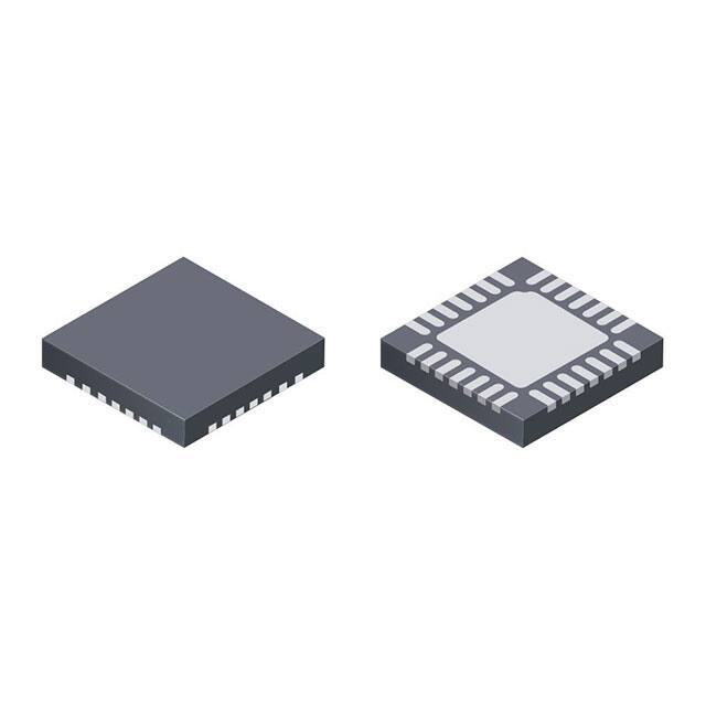
PACKAGE
28-contact QFN
with exposed thermal pad
5 mm × 5 mm × 0.90 mm
(ET package)
A field-oriented control (FOC) algorithm is fully integrated to
achieve the best efficiency and acoustic noise performance.
Constant torque and constant power modes are provided, as
well as constant speed and open-loop operating modes. The
device also optimizes the motor startup performance from a
stationary condition, a windmill condition, and even from a
reverse windmill condition.
Motor output, speed, torque, or power is controlled through
analog, PWM, or using I2C. A universal speed/power/torque/
duty curve is stored in EEPROM and allows for flexible control
schemes. An optional clock mode is available for closed-loop
speed control, with a programmable clock frequency to rpm
ratio.
The A89306 is available in a surface mount 28-contact 5 mm ×
5 mm QFN (suffix ET) package. The package has an exposed
pad for enhanced thermal dissipation, and lead (Pb) free, with
100% matte-tin leadframe plating.
Not to scale
VBB
0.1 µF
FG
SPD
FAULT
DIR
BRK
0.22 µF
CP1
CP2
0.1 µF
VCP
VBB
GHx
A89306
VREG
SENN
GLx
SENP
LSS
Figure 1: Typical Application
A89306-DS
MCO-0000798
March 19, 2020
�A89306
50 V Ultra-Low Noise FOC Motor Controller
SPECIFICATIONS
SELECTION GUIDE
Part Number
Packaging
Packing
A89306GETSR
28-contact QFN with exposed thermal pad
6000 pieces per 13-inch reel
ABSOLUTE MAXIMUM RATINGS
Characteristic
Symbol
Supply Voltage
VBB
Logic Input Voltage Range
VIN
Logic Output
VO
LSS
VLSS
VREG
VREG
Notes
Rating
Unit
50
V
SPD, BRAKE, DIR
–0.3 to 6
V
FG, FAULT (I < 5 mA)
–0.3 to 6
V
±500
mV
±4
V
DC
tW < 500 ns
0 to 4
V
±500
mV
±4
V
SA, SB, SC
–2 to VBB + 2
V
SA, SB, SC, tW < 50 ns
–4 to VBB + 4
V
DC
SENN, SENP
VSENN, VSENP
Output Voltage
VOUT
GHx
VGHx
VSx – 0.3 to VCP + 0.3
V
GLx
VGLx
VLSS – 0.3 to 8.5
V
VCP
VCP
VBB – 0.3 to VBB + 8
V
CP1
VCP1
–0.3 to VBB + 0.3
V
VCP2
VBB – 0.3 to VCP + 0.3
V
EEPROMW(MAX)
1000
cycles
CP2
Maximum EEPROM write cycles
tW < 500 ns
Junction Temperature
TJ
150
°C
Storage Temperature Range
Tstg
–55 to 150
°C
Operating Temperature Range
TA
–40 to 105
°C
Range G
THERMAL CHARACTERISTICS
Characteristic
Package Thermal Resistance
Symbol
RθJA
Test Conditions*
Value
Unit
40
°C/W
28-contact QFN (package ET), on 2-sided PCB 1-in.2 copper
*Additional thermal information available on the Allegro website.
Allegro MicroSystems
955 Perimeter Road
Manchester, NH 03103-3353 U.S.A.
www.allegromicro.com
2
�A89306
50 V Ultra-Low Noise FOC Motor Controller
22 BRAKE
23 VREG
24 SPD
25 DIR
26 FAULT
27 FG
28 SENN
PINOUT DIAGRAM AND TERMINAL LIST TABLE
SENP
1
21 NC
GND
2
20 CP1
NC
3
GLA
4
GLB
5
17 VBB
GLC
6
16 NC
LSS
7
15 VCP
19 CP2
NC 14
GHC 13
18 NC
SC 12
GHB 11
SB 10
GHA 9
SA 8
PAD
ET Package Pinouts
Terminal List Table
Number
Name
Function
19
CP2
Charge pump
20
CP1
Charge pump
22
BRAKE
Logic input
23
VREG
2.8 V regulator voltage
24
SPD
PWM or clock mode speed control
25
DIR
Direction control
26
FAULT
Fault indicator output
27
FG
28
SENN
Motor speed output
Current sense negative terminal
1
SENP
Current sense positive terminal
2
GND
Ground
4
GLA
Low-side gate drive output
5
GLB
Low-side gate drive output
6
GLC
Low-side gate drive output
7
LSS
Low-side source
8
SA
9
GHA
10
SB
11
GHB
12
SC
Motor output
High-side gate drive output
Motor output
High-side gate drive output
Motor output
13
GHC
3, 14, 16,
18, 21
High-side gate drive output
NC
No connect
15
VCP
Charge pump
17
VBB
Power supply
PAD
PAD
Exposed pad for enhanced thermal dissipation
Allegro MicroSystems
955 Perimeter Road
Manchester, NH 03103-3353 U.S.A.
www.allegromicro.com
3
�A89306
50 V Ultra-Low Noise FOC Motor Controller
FUNCTIONAL BLOCK DIAGRAM
0.1 µF X5R
CP1
CP2
0.22 µF X5R 10 V
VREG
2.8 V
VREF
VREG
7.3 V
Clock
mode
Analog to
Duty
VREF
PWM to
Duty
Charge
Pump
VBB
Universal
Curve
HSD
SPD
VREF
OCP
SDA
GATE
DRIVE
Demand
Control
I2C
BRAKE
VREF
DIR
FAULT
VBB
GHA
GHB
GHC
SCL
FG
0.1 µF X5R
VCP
LSD
EEPROM
Control
Logic
FOC
Controller
6
SA
SB
SC
GLA
GLB
GLC
LSS
Current
Sense
Amp
SENP
SENN
GND
Allegro MicroSystems
955 Perimeter Road
Manchester, NH 03103-3353 U.S.A.
www.allegromicro.com
4
�A89306
50 V Ultra-Low Noise FOC Motor Controller
ELECTRICAL CHARACTERISTICS: Valid over operating ambient temperature range and voltage range, unless noted otherwise
Characteristics
Symbol
Test Conditions
Min.
Typ.
Max.
Unit
Driving
5.5
–
48
V
Operating
5.5
–
50
V
GENERAL
Supply Voltage Range
VBB
VBB Supply Current
IBB
Reference Voltage
VREG
IVREG = 0 mA
–
8
12
mA
Standby mode
–
10
20
µA
IOUT = 10 mA
2.70
2.86
2.95
V
VBB = 8 V
6.5
6.8
–
V
GATE DRIVE
High-Side Gate Drive Output
Low-Side Gate Drive Output
Gate Drive Source Current
Gate Drive Sink Current
VGH
VGL
ISO
ISI
VBB = 24 V
6.5
6.8
–
V
VBB = 8 V
6.5
7.3
–
V
VBB = 24 V
6.5
7.3
–
V
VBB = 8 V; level 0
–
15
–
mA
VBB = 8 V; level 1
–
30
–
mA
VBB = 8 V; level 2
–
55
–
mA
VBB = 8 V; level 0
–
30
–
mA
VBB = 8 V; level 1
–
60
–
mA
VBB = 8 V; level 2
–
105
–
mA
Level 0
–
1
–
V
Level 1
–
2
–
V
VDS SENSING FOR OCP
VDS Comparator Threshold
VDS_THR
MOTOR DRIVE
PWM Duty On Threshold
PWMON
Relative to target
–0.5
–
+0.5
%
PWM Duty Off Threshold
PWMOFF
Relative to target
–0.5
–
+0.5
%
PWM Input Frequency Range
fPWM(MIN)
Clock Input Frequency Range
fCLOCK
PWM input frequency setting = 0
2.5
–
100
kHz
PWM input frequency setting = 1
80
–
3200
Hz
CLOCK mode
1
–
2000
Hz
SPD Standby Threshold
(Analog Enter)
VSPD(TH_ENT)
50
100
150
mV
SPD Standby Threshold
(Analog Exit)
VSPD(TH_EXIT)
0.4
0.75
1.0
V
210
250
290
mV
–
2.5
–
V
–
9.78
–
mV
–40
–
40
mV
SPD On Threshold
VSPD(ON)
SPD Maximum
VSPD(MAX)
ON/OFF setting = 9.7%
SPD ADC Resolution
VSPDADC(RES)
SPD ADC Accuracy
VSPDADC(ACC) VSPD = 0.2 to 2.5 V
Closed-Loop Speed Accuracy
Dead Time
Motor PWM Frequency
fSPD(ACC)
PWM mode or Analog mode
Clock mode
–5
–
5
%
–0.1
–
0.1
rpm
tDT
Code = 9
–
400
–
ns
fPWM
TA = 25°C
23.3
24.4
25.3
kHz
Continued on next page...
Allegro MicroSystems
955 Perimeter Road
Manchester, NH 03103-3353 U.S.A.
www.allegromicro.com
5
�A89306
50 V Ultra-Low Noise FOC Motor Controller
ELECTRICAL CHARACTERISTICS (continued): Valid over operating ambient temperature range and voltage range,
unless noted otherwise
Characteristics
Symbol
Test Conditions
Min.
Typ.
Max.
Unit
–
4.75
4.95
V
PROTECTION
VBB Undervoltage Threshold
VBB(UVLO)
VBB Undervoltage Hysteresis
VBB(HYS)
Thermal Shutdown Temperature
Thermal Shutdown Hysteresis
VBB rising
200
300
450
mV
TJTSD
Temperature increasing
–
165
–
°C
ΔTJ
Recovery = TJTSD – ΔTJ
–
20
–
°C
SPD, FG; VIN = 0 to 5.5 V
–5
1
5
µA
–
50
–
µA
0
–
0.8
V
LOGIC, IO, I2C
Logic Input Current
IIN
Logic Input Low Level
VIL
BRK, DIR; VIN = 5 V
Logic Input High Level
VIH
2.0
–
5.5
V
Logic Input Hysteresis
VHYS
150
300
600
mV
Logic Output Leakage
ILEAK
FG, FAULT, V = 5.5 V, switch off
–
–
1
µA
Logic Output Saturation Voltage
VSAT
FG, FAULT, I = 5 mA
–
–
0.3
V
[1]
Specified limits are tested at 25°C and 125°C and statistically assured over operating temperature range by design and characterization.
Allegro MicroSystems
955 Perimeter Road
Manchester, NH 03103-3353 U.S.A.
www.allegromicro.com
6
�A89306
50 V Ultra-Low Noise FOC Motor Controller
FUNCTIONAL DESCRIPTION
The A89306 is a three-phase BLDC controller with integrated
gate driver. It operates from 5.5 to 50V, and targets ceiling, pedestal, bathroom exhaust, air purifier, humidifier, and dehumidifier
fans, and home appliance fans and pumps.
The integrated FOC control algorithm achieves the best efficiency and dynamic response and minimizes acoustic noise.
Allegro’s proprietary non-reverse startup algorithm improves the
startup performance. The motor will start up towards the target
direction after power up without reverse shaking or vibration.
Three-phase modulation and deadtime compensation are used to
provide the lowest acoustic noise, even at very low speeds. The
optional Soft-On and Soft-Off features gradually increase the current to the motor at “on” command during a windmill condition
(when the motor is already rotating in the correct direction), and
gradually reduces the current from the motor at the “off” command, further reducing the acoustic noise and operating the motor
smoothly.
PWM Mode: In this mode, the output to the motor is controlled
by the PWM duty cycle on the SPD terminal, and higher duty cycle
represents higher motor output (unless using the input transformer
curve, described later). If open-loop mode is selected, the output
voltage amplitude will be proportional to the PWM duty cycle.
If closed-loop speed is selected, the motor speed is proportional
to the PWM duty cycle, and 100% duty represents the speed set
by the control_loop_range setting programmed in the EEPROM.
Likewise, if closed-loop torque/current is selected, the motor
phase current is proportional to the PWM duty cycle, and 100%
duty represents the current level set by the control_loop_range
setting programmed in the EEPROM. And if closed-loop power
is selected, the power delivered to the motor is proportional to the
PWM duty cycle, and 100% duty represents the power level set by
the control_loop_range setting programmed in the EEPROM.
closed_loop_speed / closed_loop_current / closed_loop_power
= control_loop_range × duty_input
The SPD PWM frequency range is 80 Hz to 100 kHz. If the input
frequency is higher than 2.8 kHz, PWMin_range should be set to 0,
and if it is lower than 2.8 kHz, PWMin_range should be set to 1.
Analog Mode: In this mode, the motor output is controlled by
the analog voltage on the SPD terminal, with higher voltage representing higher output demand. If open-loop mode is selected,
the output voltage amplitude will be proportional to the analog
voltage input. If closed-loop speed is enabled, the motor output is
as follows:
closed_loop_speed / closed_loop_current / closed_loop_power
= control_loop_range × analog_input / SPDMAX
SPD - Speed, Torque (current), Power Control
Input demand is provided via the SPD terminal. Three SPD control modes are selectable through the EEPROM. The A89306 also
features closed-loop speed, closed-loop torque (constant phase
current), and closed-loop power functions, which can be enabled
or disabled via the EEPROM.
The SPD terminal is also used as SCL for the I2C interface. See
the I2C section for details.
CLOCK Mode: When using clock mode, closed-loop speed
is always enabled. The default input for clock mode is the SPD
terminal, but there are options to use either the DIR or BRAKE
terminals instead. Either of these options allows use of the I2C
interface and clock mode at the same time. Higher frequency on
the clock input will drive a higher motor speed as follows:
closed_loop_speed (rpm) = clock_input × speed_ctrl_ratio,
where the speed_ctrl_ratio is programmed in the EEPROM. For
example, if the ratio is 4 and the clock input frequency is 60 Hz,
the motor will operate at 240 rpm. Note the number of motor
pole-pairs must be set properly in the programming application
for the rated speed (rpm) displayed for the setting to be accurate.
Note the number of pole-pairs is saved in the programming appli-
Allegro MicroSystems
955 Perimeter Road
Manchester, NH 03103-3353 U.S.A.
www.allegromicro.com
7
�A89306
50 V Ultra-Low Noise FOC Motor Controller
cation’s setting file but is not stored in the EEPROM. Thus, after
reading the settings from a device’s EEPROM in the application,
verify the pole pairs entry is correct.
If the clock frequency commands a speed that is higher than
twice the rated speed, the A89306 treats it as a clock input error
and stops the motor.
CLOCK mode can achieve the best closed-loop speed accuracy.
When using any of the closed-loop modes, if the input demand
is higher than the maximum speed/current/power, the system can
run at the applied supply voltage and load condition, the A89306
will just provide the maximum output voltage (as long as current
limit is not triggered), or the maximum output current (if current
limit is triggered).
The input demand can also be controlled using the I2C interface. Refer to register table for more details. While in Analog
mode, PWM mode, or CLOCK mode, sending an I2C command
may cause motor speed change, unexpected startup attempts, or
operation failure. Changing from I2C mode to CLOCK (Analog,
PWM) mode requires either power cycle or enter and then exit
from standby mode.
Motor Stop and Standby Mode: If the speed demand is less
than the programmed threshold, the motor will stop.
GUI setting
On threshold
Off threshold
5.8%
7.9%
5.8%
9.7%
11.8%
9.7%
12.8%
15.0%
12.8%
19.5%
21.6%
19.5%
For example, consider 9.7% is set as the threshold. If PWM duty
is less than 9.7% (in PWM mode), or the analog voltage is less
than 243 mV (in Analog mode), or the CLOCK input frequency
is less than 9.7% of the “rated_speed” (in CLOCK mode), the IC
will stop the motor and enter the “idle” mode.
In order to enter standby two conditions must be met: the motor
must be stationary (this requirement can be removed by a setting
in the EEPROM), and the SPD terminal remains logic low (in
PWM and CLOCK mode) or the SPD analog voltage remains
less than SPDTH_ENT (in Analog mode) for longer than one second. In the case that CLOCK mode is used with a terminal other
than SPD (i.e. DIR or BRAKE), the SPD terminal is still used to
put the device in standby mode.
A rising edge on the SPD terminal will wake the IC in PWM
and CLOCK mode, and in Analog mode, the voltage on the SPD
terminal must be higher than SPDTH_EXIT to wake up the IC.
Standby Mode will turn off all circuitry including the charge
pump and VREG.
After powering on, the device will always be in the active mode
before entering standby mode.
The standby mode can be disabled in the EEPROM.
Direction Input: The DIR terminal is a logic input to control
motor direction. For logic high, the motor phases are ordered
A→B→C. For logic low, the motor phases are ordered A→C→B.
The A89306 supports changing the direction input while the motor
is running. The direction can also be controlled through register.
The direction can be controlled via I2C. When the DIR_from_reg
bit is set, the direction is controlled by the Direction bit XOR’d
with the DIR terminal.
BRAKE: A logic high signal on the BRAKE terminal turns on
all low sides for the braking function. The brake function overrides the input control. Typically, when braking, the winding
current is limited only by VBEMF/RMOTOR. The A89306 includes
an optional safe braking feature which holds off braking until
the motor speed drops to a low enough level so that the braking
current will not damage the MOSFETs. The safe braking current
level is configurable in EEPROM. If this feature is not enabled,
care should be taken to avoid stress on the MOSFETs when braking a spinning motor.
The Brake Function prevents the IC from entering standby mode.
Braking can be controlled via I2C. When the BRK_from_reg bit
is set, the BRAKE pin is ignored, and the braking function is
controlled by the BRK_input bit.
FAULT: The FAULT terminal is an open-drain output which provides motor operation fault status. If used, the terminal must be
pulled up externally and is high when there is no fault. The sink
current should be limited to 10 mA or less.
An LED and a series resistor can be installed between the FAULT
and VREG terminals for a visual indication of fault information.
VREF
FAULT
Allegro MicroSystems
955 Perimeter Road
Manchester, NH 03103-3353 U.S.A.
www.allegromicro.com
8
�A89306
50 V Ultra-Low Noise FOC Motor Controller
Fault type
FAULT terminal
LED pattern
Lock detected
low
constant on
OCP
0.67 seconds high
0.67 seconds low
slow flashing
Thermal shutdown
0.67 seconds low
0.17 seconds high
0.08 seconds low
0.17 seconds high
0.08 seconds low
0.17 seconds high
long-short-short
flashing
System error
0.08 seconds low
0.08 seconds high
0.08 seconds low
1.09 seconds high
double short flashing
OVP
0.17 seconds high
0.17 seconds low
fast flashing
Input demand below
threshold
0.25 seconds high
0.08 seconds low
0.34 seconds high
0.67 seconds low
long-short flashing
System Error: A system error occurs when VBB, the charge
pump voltage, or the internal regulator which supplies the lowside gate drivers falls below the respective undervoltage threshold. The motor outputs are disabled upon a system error and will
remain off until the voltage that caused the error rises above the
respective UVLO threshold plus hysteresis.
OVP: An OVP event occurs when VBB exceeds 47 V typical.
OVP is only an indication and the outputs are not disabled. The
indication is removed when VBB falls below the threshold.
FG: The FG terminal is an open-drain output which provides
motor speed information to the system. The open-drain output
can be pulled up to VREG or an external 3.3 or 5 V supply.
The FG terminal is also used as SDA for the I2C interface. The
first I2C command can only be written when the FG is high (i.e.
the open drain is off). After the first I2C command, the FG terminal is no longer used for speed information output, and the FG
terminal is dedicated as an SDA input for the I2C interface.
I2C command 0x00A0 to address 195 (decimal). To return the
FAULT terminal to normal operation, send the I2C command
0x0000 to address 195 (decimal).
VREG: The VREG terminal is a voltage reference (2.8 V) to
power internal digital logic and analog circuitry. VREG can be
used to power external circuitry with up to 10 mA bias current, if
desired. A ceramic capacitor with 0.22 µF or greater is required
on the terminal to stabilize the supply (X8R rating or better is
recommended).
When VREG is loaded externally, the power consumption of the
internal LDO is calculated by the equation:
PLDO = (ILOAD + IINTERNAL) × (VBB – VREG).
Ensure that the system has sufficient power dissipation and the
temperature remains within the operating temperature range. The
A89306 thermal shutdown function does not protect the LDO.
Charge pump: The VCP, CP1, and CP2 terminals are used to
generate the voltage above VBB to drive the high-side MOSFETs.
A ceramic capacitor with 0.1 µF or greater is required between
VCP and VBB and between CP1 and CP2 (X8R rating or better is
recommended).
Bus Current Sensing
A single shunt-resistor connecting between SENN and SENP is
used to measure the bus current for the FOC algorithm and current
limiting. The resistor value is about tens of a milliohm, depending
on the rated current of the system. The integrated shunt-resistor
amplifier has a gain of 14.5, and its output range is 0 to 1 V. Thus,
the voltage difference between SENN and SENP should be less
than 65 mV to prevent the signal saturation. For example, if the
rated current is 4 A, it is recommended to use a 15 mΩ sensing
resistor, so that 4 A × 15 mΩ is between 55 and 65 mV.
Use Kelvin sensing connections for the shunt resistor.
FG is default high after power on and exit from standby mode,
and it remains high for at least 9.8 ms. After the 9.8 ms, the FG
output will toggle as the motor spins. To ensure successful I2C
communication, it is recommended to issue the first I2C command within 9.8 ms after power up or exiting from standby mode.
The FG function can be disabled in the EEPROM and in that
case the FG terminal can be dedicated as the SDA signal for I2C.
If observing FG signal is required in I2C mode, the FG output
signal can be reassigned to the FAULT terminal by sending the
Lock Detect: A logic circuit monitors the motor position to
determine if motor is running as expected. If a fault is detected,
the motor drive will be disabled for the configurable tLOCK time,
Allegro MicroSystems
955 Perimeter Road
Manchester, NH 03103-3353 U.S.A.
www.allegromicro.com
9
�A89306
50 V Ultra-Low Noise FOC Motor Controller
before an auto-restart is attempted. For additional information,
refer to the application note.
Current Control: The motor’s rated current at rated speed and
normal load must be programmed to the EEPROM for proper
operation. The A89306 will limit the motor current (phase current
peak value) to 1.125 times the programmed rated current during
acceleration or increasing load, which protects the MOSFETs and
the motor. A separate current limit for startup is programmed. At
startup, the current limit increases linearly between the programmed startup current and 1.125 times the programmed rated
current, reaching 1.125 times the programmed rated current
when the motor speed reaches one half of the rated speed setting.
The following plot shows the current limit for the case when the
startup current limit is set to rated current / 2:
Input-to-Output Transformer: The A89306 implements an
optional, highly flexible input-to-output mapping ability. The
configuration is stored in EEPROM addresses 32 through 63.
Fundamentally, the transformer is a 9-bit (0 to 511) to 9-bit (0 to
511) transfer function mapping the actual input value to a different
value, and the meaning of the output value changes depending on
the selected control mode. The transformer operates in whichever
of the four control modes is selected: as a speed curve transformer,
a current/torque curve transformer, a power curve transformer, or
as a demand transformer in open-loop control mode.
If open-loop mode is selected, the specified output value determines the duty cycle applied to the motor. A value of 511 will
cause the peak voltage applied to the motor to be the maximum.
If one of the closed-loop modes is selected, the output range
is determined by the control_loop_range setting. That setting
specifies the maximum speed, torque, or power that the application requires, and corresponds to the value 511. For example, in
closed-loop speed mode, if the control_loop_range setting is set
to 1000 rpm, then a transformer output value of 255 will result in
the motor spinning at 500 rpm.
The curve is defined by corner points. The corner points specify
specific input-to-output value pairs, and the remaining points are
calculated using linear interpolation between the closest corner
points. There must always be corner point entries for the input
values 0 and 511, and up to 30 additional corner points can be
defined.
Overcurrent Protection (short protection): The VDS voltage across each power MOSFET is monitored by the A89306.
When a MOSFET is switched on, its VDS is ignored for the
programmable blank time. Also, the VDS is comparator is
always filtered with a programmable filter time. If an enabled,
MOSFET’s VDS is higher than the threshold after the blank time
and for longer than the filter time, an OCP fault is triggered and
the IC will latch all MOSFETs off.
The corner points are stored in the EEPROM, one point per
address. The 9 MSBs of the EEPROM address are the input
demand at the corner point, and the 9 LSBs of the address are the
output demand for that point.
Only as many addresses that are needed to define the desired
curve must be programmed. The last point defining the curve
must have 511 as the input value, and all the following addresses
in the EREPOM will be ignored. As many as 32 corner points
can be stored, allowing for precise control of the demand.
Allegro MicroSystems
955 Perimeter Road
Manchester, NH 03103-3353 U.S.A.
www.allegromicro.com
10
�A89306
50 V Ultra-Low Noise FOC Motor Controller
Example 1: These screenshots are taken from the A89306 application—white boxes are the entered values. This is the most trivial
example, where input = output. This is the curve that is used when the transformer is disabled. Because 511 is the input value in the
second address, the 30 following addresses are ignored.
Example 2: In this example, the control loop is set to closed-loop speed, and so the resulting rpm is shown in the last column of the
table where the curve is defined. This curve is designed to avoid this motor’s resonant frequency at 2000 rpm, and its harmonics at
4000 rpm and 6000 rpm.
Allegro MicroSystems
955 Perimeter Road
Manchester, NH 03103-3353 U.S.A.
www.allegromicro.com
11
�A89306
50 V Ultra-Low Noise FOC Motor Controller
Example 3: Hysteresis can be implemented by setting the input value of an address lower than the input value in the previous address.
In this example, as the input demand is rising, the output demand will jump to next higher level at the vertical lines on the right of
each transition. When the input demand is falling, the output demand will drop to next lower level following the vertical lines on the
left of each transition. This prevents output jitter when the input is around a boundary.
Example 4: In this example, the motor won’t turn on until the input is about 30% and will turn off when the output falls below about
20%. The output will be at maximum when the input is between about 88% to 98%, and the motor will stop when the input is > 98%.
Allegro MicroSystems
955 Perimeter Road
Manchester, NH 03103-3353 U.S.A.
www.allegromicro.com
12
�A89306
50 V Ultra-Low Noise FOC Motor Controller
Example 5: The curve can be set to control bi-directional operation as well. When the bi-directional option is selected, the output value
511 is still the highest output in one direction, but the output value 255 will stop the motor, and the output value 0 is the highest output
in the reverse direction. Here, the motor will run at half speed reverse when input demand is 0, will stop when the input is between
230 and 280, and will run at full speed forward when the input is 511.
I2C Operation and EEPROM/Register Map
The I2C interface allows the user to write to and read from the internal registers, and to program parameters into the EEPROM (writing to EEPROM is explained later in this document). The A89306 I2C 7-bit slave address, also referred to as the device ID, is fixed at
0x55. The figures below show the I2C interface timing. The I2C interface can operate at up to 400 kHz.
Upon power-up, the data in the EEPROM is loaded into a group of the internal registers (referred to as shadow registers), and those
registers control the system operation. The register values can then be overwritten via the I2C port, and this will change the system
operation on the fly. Any changes to the shadow registers will be overwritten upon the next power-up. Likewise, any changes made to
the EEPROM will have no effect until the next power-up. The one exception to this is the data defining the input transformer curve,
which does not have associated shadow registers—the data defining the curve is read directly from EEPROM during operation.
The addresses of the shadow registers are offset from their associated EEPROM addresses by 64. For example, EEPROM address 10
is loaded into shadow register 74 upon power-up. To change a parameter on the fly that is contained in EEPROM address 10, the data
must be written to register 74 using the I2C port. There are no shadow registers associated with EEPROM addresses 0 through 7, or
with addresses 32 through 63.
The following diagrams illustrate how to read and write to the registers using the I2C port.
Allegro MicroSystems
955 Perimeter Road
Manchester, NH 03103-3353 U.S.A.
www.allegromicro.com
13
�A89306
50 V Ultra-Low Noise FOC Motor Controller
Write to a register:
•
•
•
•
•
Start condition
7-bit I2C slave address (1010101), R/W Bit = 0 (write)
Internal register address
3 data bytes, MSB first
Stop condition
from slave device
Slave Address
START
SDA
A6
A5
A4 A3 A2
A1
Register Address
from slave device
Data Byte 3
from slave device
Data Byte 2
from slave device
Data Byte 1
from slave device
STOP
A0 W ACK RA7 RA6 RA5 RA4 RA3 RA2 RA1 RA0 ACK D23 D22 D21 D20 D19 D18 D17 D16 ACK D15 D14 D13 D12 D11 D10 D9 D8 ACK D7 D6 D5 D4 D3 D2 D1 D0 ACK
SCL
Figure 2: Write to an I2C register
Read from a register: a two-step process:
•
•
•
•
Start condition
7-bit I2C slave address (1010101), R/W bit = 0 (write)
Internal register address to be read
Stop condition
SDA
from slave device
Slave Address
START
A6
A5
A4 A3 A2
A1
Register Address
from slave device
STOP
A0 W ACK RA7 RA6 RA5 RA4 RA3 RA2 RA1 RA0 ACK
SCL
•
•
•
•
Start condition
7-bit I2C slave address (1010101), R/W Bit = 1 (read)
Read 3 data bytes
Stop condition
SDA
from slave device
Slave Address
START
A6
A5
A4 A3 A2
A1
A0 R
Data Byte 3
from master device
Data Byte 2
from master device
Data Byte 1
NACK (no ACK) from master device
STOP
ACK D23 D22 D21 D20 D19 D18 D17 D16 ACK D15 D14 D13 D12 D11 D10 D9 D8 ACK D7 D6 D5 D4 D3 D2 D1 D0
SCL
Figure 3: Read from an I2C register
I2C Continuous Read
Note the master sends an ACK after each byte is received. After the 3 bytes of one register address is received, the master typically
sends a NACK (no ACK) to indicate the transmission is complete. Alternatively, the master may continue reading from the next
address by sending an ACK after the last byte, and the A89306 will begin sending data byte 3 of the next higher register address on the
next clock edge. The A89306 will continue sending data from the next higher address until it receives a NACK. This allows for reading data from multiple registers quickly, without needing to write each specific address per the first step of this process. In this mode,
the I2C speed must be limited to 100 kHz.
Allegro MicroSystems
955 Perimeter Road
Manchester, NH 03103-3353 U.S.A.
www.allegromicro.com
14
�A89306
50 V Ultra-Low Noise FOC Motor Controller
REGISTER AND EEPROM MAP
Each register bit is associated with one EEPROM bit. The register address is the associated EEPROM bit address plus 64. For
example, rated_speed is in EEPROM address 8, bits[10:0]; the
associated register address is 72, bits[10:0].
In the following table, the bits that are not described should be
kept at their default values. Changing these values may cause
malfunction or damage to the part. If programming the EEPROM
with a custom programmer, it is recommended to use the A89306
application to determine the appropriate settings, save the settings
file, and use the file contents to program to the EEPROM. The
application’s settings file contains one line for each EEPROM
address, containing addresses 8 through 63, but skipping address
31 (55 lines/addresses total).
Addresses 0 through 5 and address 31 are factory-locked and cannot be changed. Addresses 6 and 7 are available for the customer
to use in any way that is useful, if desired.
Registers not shown in the table are not for users to access.
Changing the value in undocumented registers may cause malfunction or damage to the part.
EEPROM address 0, Shadow register address 64
Bits
Name
Description
15:0
info_val0
Allegro internal use (locked). No shadow register associated.
EEPROM address 1, Shadow register address 65
Bits
Name
Description
15:0
info_val1
Allegro internal use (locked). No shadow register associated.
EEPROM address 2, Shadow register address 66
Bits
Name
Description
15:0
info_val2
Allegro internal use (locked). No shadow register associated.
EEPROM address 3, Shadow register address 67
Bits
Name
Description
15:0
info_val3
Allegro internal use (locked). No shadow register associated.
EEPROM address 4, Shadow register address 68
Bits
Name
Description
15:0
info_val4
Allegro internal use (locked). No shadow register associated.
EEPROM address 5, Shadow register address 69
Bits
Name
Description
15:0
info_val5
Allegro internal use (locked). No shadow register associated.
EEPROM address 6, Shadow register address 70
Bits
Name
Description
15:0
info_val6
Available to customer for general use. No shadow register associated.
EEPROM address 7, Shadow register address 71
Bits
Name
Description
15:0
info_val7
Available to customer for general use. No shadow register associated.
Allegro MicroSystems
955 Perimeter Road
Manchester, NH 03103-3353 U.S.A.
www.allegromicro.com
15
�A89306
50 V Ultra-Low Noise FOC Motor Controller
EEPROM address 8, Shadow register address 72
Bits
Name
Description
15:15
PWMin_range
Input PWM frequency range selection
0: > 2.8 kHz
1: ≤ 2.8 kHz
14:14
Direction
Direction of motor rotation
0: A→C→B
1: A→B→C
13:13
Accelerate_range
Acceleration range used for Startup Acceleration setting (Hz/s)
0: 0 to 816
1: 0 to 12.75
12:11
Digital_Speed_Mode
SPD digital input mode
0: PWM mode
1: Clock mode (using SPD input)
2: Clock mode (using DIR input)
3: Clock mode (using BRAKE input)
10:0
Rated_speed
This is the max speed used in the application.
In clock mode, this sets the max frequency, when PMW = 100%
Rated Speed (Hz) = Rated_speed_register_value × 0.530
EEPROM address 9, Shadow register address 73
Bits
Name
Description
7:0
Startup Acceleration
Specifies the motor acceleration rate at startup.
This setting’s range is selected with the Accelerate_range setting, (Hz/s).
EEPROM address 10, Shadow register address 74
Bits
Name
Description
15:13
Startup_current
Initial startup current limit (scale factor relative to Rated Current).
1 through 7: Startup Current = Rated Current × 1/8 × (value + 1).
Do not set to 0.
11:11
SPD_mode
SPD input mode.
0: Digital (PWM or Clock mode).
1: Analog.
10:0
Rated_Current
This is the motor current when running at the Rated_speed setting.
Rated Current (mA) = Rated_current_register_value / (Sense_resistor_register_value / 125).
EEPROM address 11, Shadow register address 75
Bits
Name
Description
11:10
Startup_mode
00: 6-pulse mode
01: 2-pulse mode
10: Slight-move mode
11: Align & go
7:7
Power_Ctr_En
Power control enable
0: Disable the current limit and accelerate and decelerate buffers
1: Enable the current limit and accelerate and decelerate buffers
4:4
open_ph_protect
0: Disable the open phase protection function
1: Enable the open phase protection function
3:3
Open_Drive
Open-drive debug control
0: Normal operation
1: Motor will be driven in open loop, Rated speed is then the target speed.
Allegro MicroSystems
955 Perimeter Road
Manchester, NH 03103-3353 U.S.A.
www.allegromicro.com
16
�A89306
50 V Ultra-Low Noise FOC Motor Controller
EEPROM address 12, Shadow register address 76
Bits
Name
Description
16:16
Open_Window
Opens a window for inductance tuning – see application note
0: Normal operation
1: Window opened
4:0
PID_P
Position observer PI loop proportional constant
EEPROM address 13, Shadow register address 77
Bits
Name
Description
14:14
delay_start
Delay startup (for startup modes other than Align & go)
0: VBB must be stable within 25 ms after applying start signal
1: VBB must be stable within 100 ms after applying start signal
EEPROM address 14, Shadow register address 78
Bits
Name
Description
4:4
FG_pin_dis
0: FG terminal operates as FG (until 1st successful I2C write)
1: FG terminal disabled as FG, for I2C-only applications
EEPROM address 15, Shadow register address 79
Bits
Name
Description
16:14
Safe_Brake_thrd
Current below which to allow braking, relative to rated current
000: 1 × rated_current
001: 1/2 × rated_current
010: 1/4 × rated_current
011: 1/8 × rated_current
100: 1/16 × rated_current
101: 1/32 × rated_current
110: 1/64 × rated_current
111: 1/128 × rated_current
11:8
Deadtime_setting
Deadtime selection
0: 640 ns
1 through 15: (value + 1) × 40 ns
7:7
soft_on
0: Disabled
1: Gradually increases the current at startup during a windmilling startup
6:6
soft_off
0: Disabled
1: Gradually reduces the current at motor stop
3:2
Angle_Error_Lock
Lock detect during startup.
00: disabled
01: 5 degrees
10: 9 degrees
11: 13 degrees
Allegro MicroSystems
955 Perimeter Road
Manchester, NH 03103-3353 U.S.A.
www.allegromicro.com
17
�A89306
50 V Ultra-Low Noise FOC Motor Controller
EEPROM address 16, Shadow register address 80
Bits
Name
Description
13:12
BEMF_Lock_filter
Determines the filter time for the BEMF lock detection
00: Lock detection disabled
01: Robust
10: Medium
11: Sensitive
11:10
Declarate_buffer
Determines how quickly the output command can slew
00: No buffer
01: Fast buffer
10: Medium buffer
11: Slow buffer
9:8
Accelerate_buffer
Determines how quickly the output command can slew
00: No buffer
01: Fast buffer
10: Medium buffer
11: Slow buffer
7:6
First_cycle_speed
Determines the align duration for Align & go startup mode
00: 0.55 Hz (1.81 seconds)
01: 1.1 Hz (0.91 seconds)
10: 2.2 Hz (0.45 seconds)
11: 4.4 Hz (0.23 seconds)
5:4
OCP_Masking
OCP comparators mask/blank time. Mask/blank occurs at output on/off transition
00: No masking
01: 320 ns mask
10: 640 ns mask
11: 1280 ns mask
3:3
OCP_reset_mode
Determines when to restart motor after OCP is tripped
0: Upon motor restart
1: After 5 seconds
2:0
OCP_Enable
OCP filter time and HS/LS OCP enabling. If an overcurrent condition exists at the time the OCP mask
expires, the OCP filter time must pass before an OCP fault is triggered.
000: No Filter, HS/LS OCP Enabled
001: 120 ns, HS/LS OCP Enabled
010: 240 ns, HS/LS OCP Enabled
011: 360 ns, HS/LS OCP Enabled
100: 480 ns, HS/LS OCP Enabled
101: 480 ns, LS OCP Enabled, HS OCP Disabled
110: 480 ns, LS OCP Disabled, HS OCP Enabled
111: 480 ns, HS/LS OCP Disabled
EEPROM address 17, Shadow register address 81
Bits
Name
Description
9:9
i2c_speed_mode
Input command via I2C enable
0: IC terminals are used for user input command, according to settings
1: Speed_demand setting in this register is used for user input command
8:0
Speed_demand
Speed demand input, when i2c_speed_mode is enabled
0→511 represents 0→100%
Allegro MicroSystems
955 Perimeter Road
Manchester, NH 03103-3353 U.S.A.
www.allegromicro.com
18
�A89306
50 V Ultra-Low Noise FOC Motor Controller
EEPROM address 18, Shadow register address 82
Bits
Name
Description
15:14
drive_gate_slew
Gate driver current control. Refer to the Electronics Characterization table.
13:8
IPD_Current_Thr
IPD current threshold (A) = IPD_current_thrd_value × 0.086
EEPROM address 19, Shadow register address 83
Bits
Name
Description
15:12
mosfet_comp_falling
MOSFET CISS compensation, current falling.
Refer to the application note.
11:8
mosfet_comp_rising
MOSFET CISS compensation, current rising.
Refer to the application note.
EEPROM address 20, Shadow register address 84
Bits
Name
Description
15:8
Sense_Resistor
Sense resistor value (mΩ) = sense_resistor_value / 3.7
7:0
Rated_Voltage
Motor rated voltage (V) = Rated_voltage_register_value / 5
EEPROM address 21, Shadow register address 85
Bits
Name
Description
15:15
standby_dis
Standby mode disable
0: Normal standby operation
1: Standby mode disabled
9:8
speed_input_off_threshold
Input threshold below which the motor is turned off.
If the input transformer curve is enabled, this is applied after (to the output of) the transformer curve.
00: 9.7 %
01: 5.8 %
10: 12.8 %
11: 19.5 %
7:5
slight_mv_demand
Amplitude demand used for slight move startup mode
(%) = value × 3.2 + 2.4
Allegro MicroSystems
955 Perimeter Road
Manchester, NH 03103-3353 U.S.A.
www.allegromicro.com
19
�A89306
50 V Ultra-Low Noise FOC Motor Controller
EEPROM address 22, Shadow register address 86
Bits
Name
Description
15:15
vds_threshold_sel
Short-circuit protection VDS threshold
0: 1 V
1: 2 V
12:12
Deadtime_comp
Deadtime compensation enable
0: Disabled
1: Enabled
11:11
Lock_restart_set
How long to wait before restart after lock detect is triggered
0: 5 seconds
1: 10 seconds
10:10
vibration_lock
Vibration lock detect
0: Disabled
1: Enabled
9:9
Soft_off_4s
Soft-off duration
0: 1 second
1: 4 seconds
8:8
Brake_mode
Brake mode
0: Brake when safe, according to the Safe_brake_thrd setting
1: Always brake, 100% uncontrolled
7:6
Restart_attempt
When to restart after lock detect is triggered
00: Always
01: 3 times
10: 5 times
11: 10 times
5:0
clock_speed_ratio
The ratio between input frequency and rpm, used during clock mode.
(rpm/Hz) = clock_speed_ratio_value × 0.25.
The maximum clock_speed_ratio value is 41; higher values will cause errors.
EEPROM address 23, Shadow register address 87
Bits
Name
Description
17:17
check_curve
Input transformer curve enable
0: Input curve disabled
1: Input curve enabled
16:16
speed_cur_bidir
Input transformer curve single or bi-directional mode
0: Input curve operates in a unidirectional mode and the direction is set by the device terminal or via I2C register
1: Input curve operates in a bidirectional mode where the value 0 is the fastest reverse direction, 511 is the fasted
forward direction, and 255 will stop the motor
12:11
operation_mode
Control loop mode
00: Open loop operation, output voltage magnitude set by input demand
01: Constant torque operation, torque range is set by parameterFull (eeprom_23[10:0]) × demand (as ratio)
10: Constant speed operation, speed range is set by parameterFull (eeprom_23[10:0]) × demand (as ratio)
11: Constant power operation, power range is set by parameterFull (eeprom_23[10:0]) × demand (as ratio)
10:0
parameterFull
Used in constant speed/torque/power control loops to set the maximum control setpoint. This value is the
setpoint when the input demand is 100%.
EEPROM address 24, Shadow register address 88
Bits
Name
Description
7:0
motor_resistor
Motor phase terminal to center-tap resistance (phase-phase resistance / 2).
Allegro MicroSystems
955 Perimeter Road
Manchester, NH 03103-3353 U.S.A.
www.allegromicro.com
20
�A89306
50 V Ultra-Low Noise FOC Motor Controller
EEPROM address 25, Shadow register address 89
Bits
Name
Description
15:15
BRK_input
I2C brake mode input when BRK_from_reg = 1
0: Normal running
1: Brake mode applied
14:14
BRK_from_reg
Motor brake mode control option
0: Brake is controlled via the device terminal
1: Brake is controlled via the I2C brake register
13:13
DIR_from_reg
Motor direction control option
0: Direction is controlled via the device terminal
1: Direction is controlled via the I2C direction register
10:8
inductance_shift
Motor inductance multiplier – the inductance setting is multiplied by 2 ^ inductance_shift
7:0
inductance
Motor inductance, set along with the Inducatnce_shift setting – this value is multiplied by 2 ^ inductance_shift
EEPROM address 26, Shadow register address 90
Bits
Name
Description
8:0
Kt_set
Motor Kt constant
EEPROM address 28, Shadow register address 92
Bits
Name
Description
17:15
current_loop_I
Current PI loop integration constant
14:10
power_loop_p
Power PI loop proportional constant
9:5
speed_loop_p
Speed PI loop proportional constant
4:0
current_loop_p
Current PI loop proportional constant
EEPROM address 29, Shadow register address 93
Bits
Name
Description
5:3
power_loop_I
Power PI loop integration constant
2:0
speed_loop_I
Speed PI loop integration constant
EEPROM address 31, Shadow register address 95
Bits
Name
Description
15:0
Output_array_trim
Allegro-determined trim values (locked)
EEPROM addresses 32-63 (No shadow registers associated)
Bits
Name
Description
17:9
x_interpolation_point
Corner point input value for the input transformer curve. No shadow register associated.
8:0
y_interpolation_point
Corner point output value for the input transformer curve. No shadow register associated.
Note: Refer to application note and user interface for additional detail.
Allegro MicroSystems
955 Perimeter Road
Manchester, NH 03103-3353 U.S.A.
www.allegromicro.com
21
�A89306
50 V Ultra-Low Noise FOC Motor Controller
PROGRAMMING THE EEPROM
The A89306 contains 64 words of EEPROM, and each word is
24 bits long. The 6 most significant bits of each word are used
internally for error detection and correction (ECC), and the 18
least significant bits are used to store data. The handling of the
ECC data is done automatically by the IC, and the user does not
need to (and cannot) read or write the ECC data.
The EEPROM is programmed using the I2C interface. Before
accessing the EPEPOM, access must be enabled by writing the
value 0x000001 I2C register address 196. When done accessing the EEPROM, revert to normal operation by writing the
value 0x000000 to I2C register address 196. There are three
basic actions which can be performed on the EEPROM: read,
erase, and write. Erasing a single address in the EEPROM
requires 4 writes to the I2C port, and writing to a single address
in the EEPROM require 3 writes to the I2C port. These registers, addresses 161, 162, and 163, are described below and the
sequence for writing to these registers is described on the following page. Reading a single address from the EEPROM requires
only 1 read from the I2C port. Each EEPROM address is mapped
the corresponding I2C address. To read EEPROM address 8, for
example, simply read I2C register address 8.
Each EEPROM address must be programmed individually. To
change the contents of an EEPROM address, the word must
first be erased before the new data is written. Programming each
address requires about 45 ms (30 ms for erase and 15 ms for
write).
EEPROM Control – Register 161: Used to control programming of EEPROM
Bit
23
22
21
20
19
18
17
16
15
14
13
12
11
10
9
8
7
6
5
4
3
2
1
0
Name
0
0
0
0
0
0
0
0
0
0
0
0
0
0
0
0
0
0
0
0
RD
WR
ER
EN
3
2
1
0
1
0
Bit
Name
0
EN
Generate the high-voltage pulse required for writing or erasing. This bit self-clears when done, after 15 ms maximum.
Description
1
ER
Set this bit high when erasing data to the EEPROM.
2
WR
Set this bit high when writing data to the EEPROM.
3
RD
This bit is for reading data, but is not required for the method described in this datasheet to read the EEPROM.
23:4
n/a
Do not use; always set to zero (0) during programming process.
EEPROM Address – Register 162: Used to set the EEPROM address to be altered
Bit
23
22
21
20
19
18
17
16
15
14
13
12
11
10
9
8
7
6
Name
0
0
0
0
0
0
0
0
0
0
0
0
0
0
0
0
0
0
7
6
Bit
Name
5:0
eeADDRESS
23:6
n/a
5
4
eeADDRESS
Description
Used to specify the EEPROM address to be erased or written. There are 64 addresses.
Do not use; always set to zero (0) during programming process.
EEPROM Data_In – Register 163: Used to set the new EEPROM data to be programmed
Bit
23
22
21
20
19
18
Name
0
0
0
0
0
0
Bit
Name
17:0
eeDATAin
23:18
n/a
17
16
15
14
13
12
11
10
9
8
5
4
3
2
eeDATAin
Description
Used to specify the new EEPROM data. This must be set to 0 when erasing the current contents.
Do not use; always set to zero (0) during programming process.
Allegro MicroSystems
955 Perimeter Road
Manchester, NH 03103-3353 U.S.A.
www.allegromicro.com
22
�A89306
50 V Ultra-Low Noise FOC Motor Controller
Programming the EEPROM Examples
The example below is shown in the following format:
I2C Write/Read, I2C_register_address [data] // comment
*Before accessing the EEPROM, the value 0x000001 must be written to I2C address 196.
Example #1: Write 261 (0x000105) to EEPROM address 7
1. Erase the existing data:
A. I2C Write, 162 [7]
// set which EEPROM address to erase.
B. I2C
Write, 163 [0]
// set Data_In = 0x000000.
C. I2C
Write, 161 [3]
// set control to erase and set voltage high.
D. Wait 15 ms
// requires 15 ms high-voltage pulse to erase.
E. I2C Write, 161 [3]
// set control to erase and set voltage high.
F. Wait 15 ms
// requires 15 ms high-voltage pulse to erase.
2. Write the new data:
A. I2C Write, 162 [7]
// set which EEPROM address to write.
B. I2C
Write, 163 [261]
// set Data_In = 261 (0x000105).
C. I2C
Write, 161 [5]
// set control to write and set voltage high.
D. Wait 15 ms
// requires 15 ms high-voltage pulse to write.
Example #2: Read EEPROM address 7 to confirm the data was properly programmed
1. Read the word:
A. I2C Read, 7
// read I2C register 7; this will be contents of EEPROM address 7.
*When done accessing the EEPROM, write the value 0x000000 to I2C address 196.
Allegro MicroSystems
955 Perimeter Road
Manchester, NH 03103-3353 U.S.A.
www.allegromicro.com
23
�A89306
50 V Ultra-Low Noise FOC Motor Controller
TERMINAL DIAGRAMS
DIR
2 kΩ
VBB
BRAKE
10 V
6.5 V
100 kΩ
8V
56 V
VCP
2 kΩ
GHx
SPD
10 V
10 V
6.5 V
Sx
FG
FAULT
10 V
VBB
VREFINT
(internal regulator)
VBB
8V
GLx
VREF
LSS
6V
CP2
VCP
VBB
SENP
CP1
6V
VBB
SENN
6V
7V
Figure 4: Terminal Diagrams
Allegro MicroSystems
955 Perimeter Road
Manchester, NH 03103-3353 U.S.A.
www.allegromicro.com
24
�A89306
50 V Ultra-Low Noise FOC Motor Controller
PACKAGE OUTLINE DRAWING
0.30
5.00 ±0.15
1.15
28
1
2
0.50
28
1
A
5.00 ±0.15
3.15
4.80
3.15
29X
D
SEATING
PLANE
0.08 C
+0.05
0.25 –0.07
0.90 ±0.10
C
4.80
C
PCB Layout Reference View
0.50
+0.20
0.55 –0.10
B
3.15
2
1
XXXX
Date Code
Lot Number
E Standard Branding Reference View 1
28
3.15
For Reference Only
(reference JEDEC MO-220VHHD-1)
Dimensions in millimeters
Exact case and lead configuration at supplier discretion within limits shown
Line 1: Part Number
Line 2: Logo A, 4-Digit Date Code
Line 3: Characters 5, 6, 7, 8 of Assembly Lot Number
A Terminal #1 mark area.
B Exposed thermal pad (reference only, terminal #1
identifier appearance at supplier discretion).
C Reference land pattern layout (reference IPC7351
QFN50P500X500X100-29V1M);
All pads a minimum of 0.20 mm from all adjacent pads; adjust as
necessary to meet application process requirements and PCB layout
tolerances; when mounting on a multilayer PCB, thermal vias at the
exposed thermal pad land can improve thermal dissipation (reference
EIA/JEDEC Standard JESD51-5).
D Coplanarity includes exposed thermal pad and terminals.
E Branding scale and appearance at supplier discretion.
Figure 5: Package ET, 28-Contact QFN with Exposed Pad
Allegro MicroSystems
955 Perimeter Road
Manchester, NH 03103-3353 U.S.A.
www.allegromicro.com
25
�A89306
50 V Ultra-Low Noise FOC Motor Controller
Revision History
Number
Date
Description
–
March 19, 2020
Preliminary
Copyright 2020, Allegro MicroSystems.
Allegro MicroSystems reserves the right to make, from time to time, such departures from the detail specifications as may be required to permit
improvements in the performance, reliability, or manufacturability of its products. Before placing an order, the user is cautioned to verify that the
information being relied upon is current.
Allegro’s products are not to be used in any devices or systems, including but not limited to life support devices or systems, in which a failure of
Allegro’s product can reasonably be expected to cause bodily harm.
The information included herein is believed to be accurate and reliable. However, Allegro MicroSystems assumes no responsibility for its use; nor
for any infringement of patents or other rights of third parties which may result from its use.
Copies of this document are considered uncontrolled documents.
For the latest version of this document, visit our website:
www.allegromicro.com
Allegro MicroSystems
955 Perimeter Road
Manchester, NH 03103-3353 U.S.A.
www.allegromicro.com
26
�


 工商网监
湘ICP备2023018690号
工商网监
湘ICP备2023018690号
