AS4C8M32MD2A-25BPCN
Revision History
8M x 32 Mobile DDR2 AS4C8M32MD2A-25BPCN - 168 ball POP
FBGA PACKAGE
Revision
Rev 1.0
Rev 1.2
Details
Date
Preliminary datasheet
Feb 2018
Part number typo was AS4C8M32MD2A-25B2CN should be
May 2019
AS4C8M32MD2A-25BPCN. Also added-in word 'POP' missing in
package descriptions for the FBGA package
Alliance Memory Inc. 511 Taylor Way, San Carlos, CA 94070 TEL: (650) 610-6800 FAX: (650) 620-9211
Alliance Memory Inc. reserves the right to change products or specification without notice
Confidential
-1-
Rev.1.1. May.2019
�AS4C8M32MD2A-25BPCN
8M x 32 Mobile LPDDR2 Synchronous DRAM (SDRAM)
(Rev. 1.1, May. /2019)
Alliance Memory Confidential
Features
Overview
Fast clock rate: 400 MHz
Differential Clock inputs CK/CK#
JEDEC standard Compliant
Four-bit prefetch DDR architecture
Four internal banks, 2M x 32-bit for each bank
Double data rate architecture for command, address
and data Bus
Bidirectional/differential data strobe per byte of data
DQS/DQS#
Programmable Mode Registers
- READ and WRITE latencies (RL/WL)
- Burst length: 4, 8, or 16
- PASR (Partial Array Self Refresh)
Auto TCSR (Temperature Compensated Self Refresh)
Auto Refresh and Self Refresh
Deep power-down
4096 refresh cycles / 32ms
Power supplies:
- VDD1 = 1.8V (1.7V~1.95V)
- VDD2 = 1.2V (1.14V~1.3V)
- VDDCA /VDDQ = 1.2V (1.14V~1.3V)
Interface: HSUL_12
Operating Temperature: TC = -25 ~ 85C
Package: 168-ball 12 x 12 x 0.9mm (max) POP FBGA
- Pb Free and Halogen Free
The AS4C8M32MD2A-25BPCN LPDDR2 SDRAM is
a high-speed CMOS, dynamic random-access
memory containing 268,435,456 bits. It is internally
configured as a 4 banks of 2,097,152 words by 32
bits memory device. The devices use double data
rate architecture on the command/address (CA)
bus to reduce the number of input pins in the
system. The 10-bit CA bus contains command,
address, and Bank/Row Buffer information. Each
command uses one clock cycle, during which
command information is transferred on both the
positive and negative edge of the clock. LPDDR2
also use double data rate architecture on the DQ
pins to achieve high speed operation. The double
data rate architecture is essentially a 4n
prefetch architecture with an interface designed
to transfer two data bits per DQ every clock cycle at
the I/O pins. A single read or write access for
the LPDDR2 effectively consists of a single 4n-bit
wide, one clock cycle data transfer at the internal
SDRAM/NVM core and four corresponding n-bit
wide, one-half-clock-cycle data transfers at the I/O
pins. Read and write accesses to the LPDDR2 are
burst oriented; accesses start at a selected location
and continue for a programmed number of locations
in a programmed sequence.
Table 1. Ordering Information
Part Number
Org
AS4C8M32MD2A-25BPCN
8Mx32
Temperature
MaxClock (MHz)
Commercial Extended -25°C to +85°C
400
Package
168-ball POP FBGA
Table 2. Speed Grade Information
Speed Grade
DDR2L-800
Confidential
Clock Frequency
RL
WL
tRCD (ns)
tRP (ns)
400MHz
6
3
18
18
-2-
Rev.1.1. May.2019
�AS4C8M32MD2A-25BPCN
Figure 1. Ball Assignment (POP FBGA Top View)
Package code: BP - 168-ball 12 x 12 x 0.9mm (max) POP FBGA
1
2
3
4
5
6
7
8
9
10
11
12
13
14
15
16
18
19
20
21
22
23
A
NC
NC
NC
NC
NC
NC
NC
NC
NC
NC
VDD1
VSSQ
DQ30
DQ29
VSSQ
DQ26
DQ25
VSSQ
DQS3#
VDD1
VSS
NC
NC
B
NC
NC
VDD1
NC
VSS
NC
NC
VSS
NC
VSS
VDD2
DQ31
VDDQ
DQ28
DQ27
VDDQ
DQ24
DQS3
VDDQ
DM3
VDD2
NC
NC
C
VSS
VDD2
DQ15
VSSQ
D
NC
NC
VDDQ
DQ14
E
NC
NC
DQ12
DQ13
F
NC
VSS
DQ11
VSSQ
G
NC
NC
VDDQ
DQ10
H
NC
NC
DQ8
DQ9
J
NC
VSS
DQS1
VSSQ
K
NC
NC
VDDQ
DQS1#
L
NC
NC
VDD2
DM1
M
NC
VSS
VREFDQ
VSS
N
NC
VDD1
VDD1
DM0
P
ZQ
VREFCA
DQS0#
VSSQ
R
VSS
VDD2
VDDQ
DQS0
T
CA9
CA8
DQ6
DQ7
U
CA7
VDDCA
DQ5
VSSQ
V
VSSCA
CA6
VDDQ
DQ4
W
CA5
VDDCA
DQ2
DQ3
Y
CK#
CK
DQ1
VSSQ
AA
VSS
VDD2
VDDQ
DQ0
AB
NC
NC
CS#
NC
VDD1
CA1
VSSCA
CA3
CA4
VDD2
VSS
DQ16
VDDQ
DQ18
DQ20
VDDQ
DQ22
DQS2
VDDQ
DM2
VDD2
NC
NC
AC
NC
NC
CKE
NC
VSS
CA0
CA2
VDDCA
VSS
NC
NC
VSSQ
DQ17
DQ19
VSSQ
DQ21
DQ23
VSSQ
DQS2#
VDD1
VSS
NC
NC
Confidential
-3-
17
Rev.1.1. May.2019
�AS4C8M32MD2A-25BPCN
Figure 2. Block Diagram
CLOCK
BUFFER
CKE
PASR, TCSR, DS
EXTENDED
MODE
REGISTER
Row
Decoder
CK
CK#
2M x 32
CELL ARRAY
(BANK #0)
Column Decoder
SELF REFRESH
LOGIC & TIMER
CS#
CA0~9
COMMAND/
ADDRESS
DECODER
Row
Decoder
CONTROL
SIGNAL
GENERATOR
2M x 32
CELL ARRAY
(BANK #1)
Column Decoder
MODE
REGISTER
ADDRESS
BUFFER
Row
Decoder
COLUMN
COUNTER
2M x 32
CELL ARRAY
(BANK #2)
Column Decoder
DQS0~3
DQS0#~3#
DATA
STROBE
BUFFER
DQ
Buffer
DQ0~31
Row
Decoder
REFRESH
COUNTER
2M x 32
CELL ARRAY
(BANK #3)
Column Decoder
DM0~3
Confidential
-4-
Rev.1.1. May.2019
�AS4C8M32MD2A-25BPCN
Figure 3. State Diagram
Power
applied
Power
On
Automatic Sequence
Command Sequence
Deep
Power
Down
DPDX
R
e
es
Self
Refreshing
t
Resetting
MR
Reading
MRR
Resetting
DPD
EF X
SRREF
S
R
et
es
PD X
PD
Idle*1
Resetting
Power
Down
REF
Refreshing
R
MR
X
PD
MR
W
Idle
MR
Reading
PD
MR
Writing
Active
Power
Down
PR
MR
Active
R
BST
RD
RD
WR
W
RA
Reading
PR, PRA
A
RD
PR(A) = Precharge (All)
ACT = Activate
Writing
WR(A) = Write (with Auto precharge)
RD(A) = Read (with Auto precharge)
BST = Burst Terminate
Reset = Reset is achieved through MRW command
MRW = Mode Register Write
WRA
MRR = Mode Register Read
PD = Enter Power Down
PDX = Exit Power Down
SREF = Enter Self Refresh
Writing
SREFX = Exit Self Refresh
With
DPD = Enter Deep Power Down
Auto precharge
DPDX = Exit Deep Power Down
REF = Refresh
Idle
Power
Down
Active
MR
Reading
PD
PD X
BST
WR
ACT
RDA
Reading
With
Auto precharge
Precharging
NOTE 1. All banks are precharged in the idle state.
Confidential
-5-
Rev.1.1. May 2019
�AS4C8M32MD2A-25BPCN
Ball Descriptions
Table 2. Ball Details
Symbol
Type
Description
CK, CK#
Input
Differential Clock: CK and CK# are differential clock inputs. All CA inputs are
sampled on both rising and falling edges of CK. CS# and CKE inputs are sampled
at the rising edge of CK. AC timings are referenced to clock.
CKE
Input
CS#
Input
Clock Enable: CKE HIGH activates and CKE LOW deactivates the internal clock
signals, input buffers, and output drivers. Power-saving modes are entered and
exited via CKE transitions. CKE is considered part of the command code. CKE is
sampled at the rising edge of CK.
Chip Select: CS# is considered part of the command code and is sampled at the
rising edge of CK.
CA0 – CA9
Input
DQ0 – DQ31
Input /
Output
Data input/output: Bidirectional data bus.
DQS0 – DQS3
Input /
Output
Data Strobe: The data strobe is bi-directional (used for read and write data) and
differential (DQS and DQS#). It is output with read data and input with write data.
DQS is edge-aligned to read data and centered with write data.
DQS0 and DQS0# correspond to the data on DQ0 - DQ7.
DQS1 and DQS1# correspond to the data on DQ8 - DQ15.
DQS2 and DQS2# correspond to the data on DQ16 – DQ23.
DQS3 and DQS3# correspond to the data on DQ24 – DQ31.
Input Data Mask: DM is an input mask signal for write data. Although DM balls are
input-only, the DM loading is designed to match that of DQ and DQS balls.
DM0 is the input data mask signal for the data on DQ0-7.
DM1 is the input data mask signal for the data on DQ8-15.
DM2 is the input data mask signal for the data on DQ16 – DQ23.
DM3 is the input data mask signal for the data on DQ24 – DQ31.
DQS0# – DQS3#
DDR Command/Address Inputs: Provide the command and address inputs
according to the command truth table.
DM0 – DM3
Input
VDDQ
Supply
DQ Power Supply: Provide isolated power to DQs for improved noise immunity.
VSSQ
Supply
DQ Ground: Provide isolated ground to DQs for improved noise immunity.
VDDCA
Supply
Command/address power supply: Command/address power supply.
VSSCA
Supply
Ground for Input Receivers
VDD1
Supply
Core power: Supply 1.
VDD2
Supply
Core power: Supply 2.
VSS
Supply
Ground
VREFCA, VREFDQ
Supply
Reference voltage: VREFCA is reference for command/address input buffers,
VREFDQ is reference for DQ input buffers.
ZQ
NC
Confidential
Reference Reference Pin for Output Drive Strength Calibration
-
No Connect: No internal connection.
-6-
Rev.1.1. May 2019
�AS4C8M32MD2A-25BPCN
Truth Tables
Operation or timing that is not specified is illegal and after such an event, in order to guarantee proper operation,
the device must be powered down and then restarted through the specified initialization sequence before normal
operation can continue.
Table 3. Command Truth Table
Command
Command Pins
CKE
CS#
CKn-1
CKn
MRW
H
H
MRR
H
H
Refresh
(All bank)
H
H
Enter
Self Refresh
H
Activate
H
H
Write
H
H
Read
H
H
Precharge
H
H
BST
H
H
Enter
DPD
H
NOP
H
H
Maintain
PD, SREF, DPD
(NOP)
L
L
NOP
H
H
Maintain
PD, SREF, DPD
(NOP)
L
L
X
X
Enter
Power Down
H
Exit
PD, SREF, DPD
L
Confidential
X
X
L
L
L
H
CA Pins
CA0
CA1
CA2
CA3
CA4
CA5
CA6
CA7
CA8
CA9
L
L
L
L
L
MA0
MA1
MA2
MA3
MA4
MA5
X
MA6
MA7
OP0
OP1
OP2
OP3
OP4
OP5
OP6
OP7
L
L
L
L
H
MA0
MA1
MA2
MA3
MA4
MA5
X
MA6
MA7
X
X
X
X
X
X
X
X
L
L
L
H
H
X
X
X
X
X
X
X
X
X
X
X
X
X
X
X
X
X
L
L
L
H
X
X
X
X
X
X
X
X
X
X
X
X
X
X
X
X
X
X
L
L
H
R8
R9
R10
R11
R12
BA0
BA1
X
X
R0
R1
R2
R3
R4
R5
R6
R7
X
X
L
H
L
L
RFU
RFU
C1
C2
BA0
BA1
X
X
AP
C3
C4
C5
C6
C7
X
X
X
X
L
H
L
H
RFU
RFU
C1
C2
BA0
BA1
X
X
AP
C3
C4
C5
C6
C7
X
X
X
X
L
H
H
L
H
AB
X
X
BA0
BA1
X
X
X
X
X
X
X
X
X
X
X
X
L
H
H
L
L
X
X
X
X
X
X
X
X
X
X
X
X
X
X
X
X
X
L
H
H
L
X
X
X
X
X
X
X
X
X
X
X
X
X
X
X
X
X
X
L
H
H
H
X
X
X
X
X
X
X
X
X
X
X
X
X
X
X
X
X
X
L
H
H
H
X
X
X
X
X
X
X
X
X
X
X
X
X
X
X
X
X
X
H
X
X
X
X
X
X
X
X
X
X
X
X
X
X
X
X
X
X
X
X
X
H
X
X
X
X
X
X
X
X
X
X
X
X
X
X
X
X
X
X
X
X
X
H
X
X
X
X
X
X
X
X
X
X
X
X
X
X
X
X
X
X
X
X
X
H
X
X
X
X
X
X
X
X
X
X
X
X
X
X
X
X
X
X
X
X
X
-7-
CK
Edge
Rev.1.1. May 2019
�AS4C8M32MD2A-25BPCN
Notes:
1. All commands are defined by the current state of CS#, CA0, CA1, CA2, CA3, and CKE at the rising edge of the
clock.
2. Bank addresses (BA) determine which bank will be operated upon.
3. AP HIGH during a READ or WRITE command indicates that an auto precharge will occur to the bank
associated with the READ or WRITE command.
4. “X” indicates a “Don’t Care” state, with a defined logic level, either HIGH (H) or LOW (L).
5. Self refresh exit and DPD exit are asynchronous.
6. VREF must be between 0 and VDDQ during self refresh and DPD operation.
7. CAxr refers to command/address bit “X” on the rising edge of clock.
8. CAxf refers to command/address bit “X” on the falling edge of clock.
9. CS# and CKE are sampled on the rising edge of the clock.
10. The least-significant column address C0 is not transmitted on the CA bus, and is inferred to be zero.
Confidential
-8-
Rev.1.1. May 2019
�AS4C8M32MD2A-25BPCN
Table 4. CKE Truth Table
Notes 1–5 apply to all parameters and conditions; L = LOW, H = HIGH, X = “Don’t Care”
Current
State
CKn-1
CKn
CS#
Command n
Operation n
Next State
Active
power-down
L
L
X
X
Maintain active powerdown
Active
power-down
L
H
H
NOP
Exit active power-down
Active
Idle
power-down
L
L
X
X
Maintain active powerdown
Idle
power-down
L
H
H
NOP
Exit idle power-down
Idle
Resetting idle
power-down
L
L
X
X
Maintain resetting powerdown
Resetting
power-down
L
H
H
NOP
Exit resetting power-down
Idle or resetting
Deep
power-down
L
L
X
X
Maintain deep power-down
Deep
power-down
L
H
H
NOP
Exit deep power-down
Power-on
L
L
X
X
Maintain self refresh
Self refresh
L
H
H
NOP
Exit self refresh
Idle
H
L
H
NOP
Enter active power-down
H
L
H
NOP
Enter idle power-down
H
L
L
Enter self
refresh
Enter self refresh
H
L
L
DPD
Enter self refresh
Resetting
H
L
H
NOP
Enter resetting powerdown
Other states
H
H
Self refresh
Bank active
All banks idle
Note
6, 7
6, 7
6, 7, 8
9
10, 11
Active
power-down
Idle
power-down
Self refresh
Deep
power-down
Resetting
power-down
Refer to the command truth table
Notes:
1. Current state = the state of the device immediately prior to the clock rising edge n.
2. All states and sequences not shown are illegal or reserved unless explicitly described elsewhere in this document.
3. CKEn = the logic state of CKE at clock rising edge n; CKEn-1 was the state of CKE at the previous clock edge.
4. CS# = the logic state of CS# at the clock rising edge n.
5. Command n = the command registered at clock edge n, and operation n is a result of command n.
6. Power-down exit time (tXP) must elapse before any command other than NOP is issued.
7. The clock must toggle at least twice prior to the tXP period.
8. Upon exiting the resetting power-down state, the device will return to the idle state if tINIT5 has expired.
9. The DPD exit procedure must be followed as described in Deep Power-Down.
10. Self refresh exit time (tXSR) must elapse before any command other than NOP is issued.
11. The clock must toggle at least twice prior to the tXSR time.
Confidential
-9-
Rev.1.1. May 2019
�AS4C8M32MD2A-25BPCN
Table 5. Current State Bank n - Command to Bank n
Notes 1–5 apply to all parameters and conditions
Current
State
Any
Idle
Row active
Reading
Writing
Power-on
Command
Operation
Next State
Note
NOP
Continue previous operation
Current state
ACTIVATE
Select and activate row
Active
Refresh (all banks)
Begin to refresh
Refreshing (all banks)
6
MRW
Load value to mode register
MR writing
6
MRR
Read value from mode register
Idle, MR reading
RESET
Begin device auto initialization
Resetting
6, 7
PRECHARGE
Deactivate row(s) in bank or banks
Precharging
8, 9
READ
Select column and start read burst
Reading
WRITE
Select column and start write burst
Writing
MRR
Read value from mode register
Active MR reading
PRECHARGE
Deactivate row(s) in bank or banks
Precharging
READ
Select column and start new read burst
Reading
10, 11
WRITE
Select column and start write burst
Writing
BST
Read burst terminate
Active
10, 11,
12
13
WRITE
Select column and start new write burst
Writing
10, 11
READ
Select column and start read burst
Reading
BST
Write burst terminate
Active
10, 11,
14
13
MRW RESET
Begin device auto initialization
Resetting
8
6, 8
Resetting
MRR
Read value from mode register
Resetting MR reading
Notes:
1. Values in this table apply when both CKE n-1 and CKEn are HIGH, and after tXSR or tXP has been met, if the
previous state was power-down.
2. All states and sequences not shown are illegal or reserved.
3. Current state definitions:
Idle: The bank or banks have been precharged, and tRP has been met.
Active: A row in the bank has been activated, and tRCD has been met. No data bursts or accesses and no register
accesses are in progress.
Reading: A READ burst has been initiated with auto precharge disabled and has not yet terminated or been terminated.
Writing: A WRITE burst has been initiated with auto precharge disabled and has not yet terminated or been terminated.
4. The states listed below must not be interrupted by a command issued to the same bank. NOP commands or
supported commands to the other bank must be issued on any clock edge occurring during these states.
Supported commands to the other banks are determined by that banks current state.
Precharge: Starts with registration of a PRECHARGE command and ends when tRP is met. After tRP is met, the bank is in
the idle state.
Row activate: Starts with registration of an ACTIVATE command and ends when tRCD is met. After tRCD is met, the bank
is in the active state.
READ with AP enabled: Starts with registration of a READ command with auto precharge enabled and ends when tRP is
met. After tRP is met, the bank is in the idle state.
WRITE with AP enabled: Starts with registration of a WRITE command with auto precharge enabled and ends when tRP is
met. After tRP is met, the bank is in the idle state.
Confidential
- 10 -
Rev.1.1. May 2019
�AS4C8M32MD2A-25BPCN
5. The states listed below must not be interrupted by any executable command. NOP commands must be applied
to each rising clock edge during these states.
Refresh (all banks): Starts with registration of a REFRESH (all banks) command and ends when tRFCab is met. After
tRFCab is met, the device is in the all banks idle state.
Idle MR reading: Starts with registration of the MRR command and ends when tMRR is met. After tMRR is met, the device
is in the all banks idle state.
Resetting MR reading: Starts with registration of the MRR command and ends when tMRR is met. After tMRR is met, the
device is in the all banks idle state.
Active MR reading: Starts with registration of the MRR command and ends when tMRR is met. After tMRR is met, the bank
is in the active state.
MR writing: Starts with registration of the MRW command and ends when tMRW is met. After tMRW is met, the device is in
the all banks idle state.
Precharging all: Starts with registration of a PRECHARGE ALL command and ends when tRP is met. After tRP is met, the
device is in the all banks idle state.
6. Not bank-specific; requires that all banks are idle and no bursts are in progress.
7. Not bank-specific.
8. This command may or may not be bank specific. If all banks are being precharged, they must be in a valid state
for precharging.
9. If a PRECHARGE command is issued to a bank in the idle state, tRP still applies.
10. A command other than NOP should not be issued to the same bank while a burst READ or burst WRITE with
auto precharge is enabled.
11. The new READ or WRITE command could be auto precharge enabled or auto precharge disabled.
12. A WRITE command can be issued after the completion of the READ burst; otherwise, a BST must be issued to
end the READ prior to asserting a WRITE command.
13. Not bank-specific. The BST command affects the most recent READ/WRITE burst started by the most recent
READ/WRITE command, regardless of bank.
14. A READ command can be issued after completion of the WRITE burst; otherwise, a BST must be used to end
the WRITE prior to asserting another READ command.
Confidential
- 11 -
Rev.1.1. May 2019
�AS4C8M32MD2A-25BPCN
Table 6. Current State Bank n - Command to Bank m
Notes 1–6 apply to all parameters and conditions
Current State
of Bank n
Any
Idle
Command to
Bank m
NOP
Any
ACTIVATE
READ
Row activating,
Active or
precharging
WRITE
PRECHARGE
MRR
BST
Reading
(auto precharge
disabled)
Writing
(auto precharge
disabled)
Reading with
auto precharge
Writing with
auto precharge
Power-on
Resetting
READ
WRITE
ACTIVATE
PRECHARGE
READ
WRITE
ACTIVATE
PRECHARGE
READ
WRITE
Operation
Continue previous operation
Any command supported to bank m
Select and activate row in bank m
Select column and start READ burst
from bank m
Select column and start WRITE burst to
bank m
Deactivate row(s) in bank or banks
READ value from mode register
READ or WRITE burst terminates an
ongoing READ/WRITE from/to bank m
Select column and start READ burst
from bank m
Select column and start WRITE burst to
bank m
Select and activate row in bank m
Deactivate row(s) in bank or banks
Select column and start READ burst
from bank m
Select column and start WRITE burst to
bank m
Select and activate row in bank m
Deactivate row(s) in bank or banks
Select column and start READ burst
from bank m
Select column and start WRITE burst to
bank m
Next State for Bank m
Current state of bank m
Active
Reading
Precharging
Idle MR reading or active
MR reading
Reading
Writing
Active
Precharging
Reading
Writing
Active
Precharging
Reading
Writing
ACTIVATE
PRECHARGE
READ
Select and activate row in bank m
Deactivate row(s) in bank or banks
Select column and start READ burst
from bank m
Active
Precharging
Reading
WRITE
Writing
ACTIVATE
PRECHARGE
MRW RESET
Select column and start WRITE burst to
bank m
Select and activate row in bank m
Deactivate row(s) in bank or banks
Begin device auto initialization
MRR
Read value from mode register
Resetting MR reading
Active
Precharging
Resetting
7
8
9
9
Writing
Active
Note
10
11,
12,
13
7
9
9,
14
10
9,
15
9
10
9,
16
9,
14,
16
10
9,
15,
16
9,
16
10
17,
18
Notes:
1. This table applies when: the previous state was self refresh or power-down; after tXSR or tXP has been met;
and both CKEn -1 and CKEn are HIGH.
2. All states and sequences not shown are illegal or reserved.
3. Current state definitions:
Idle: The bank has been precharged and tRP has been met.
Active: A row in the bank has been activated, tRCD has been met, no data bursts or accesses and no register accesses
are in progress.
Read: A READ burst has been initiated with auto precharge disabled and the READ has not yet terminated or been terminated.
Write: A WRITE burst has been initiated with auto precharge disabled and the WRITE has not yet terminated or been
terminated.
4. Refresh, self refresh, and MRW commands can only be issued when all banks are idle.
5. A BST command cannot be issued to another bank; it applies only to the bank represented by the current state.
Confidential
- 12 -
Rev.1.1. May 2019
�AS4C8M32MD2A-25BPCN
6. The states listed below must not be interrupted by any executable command. NOP commands must be applied
during each clock cycle while in these states:
Idle MRR: Starts with registration of the MRR command and ends when tMRR has been met. After tMRR is met, the device
is in the all banks idle state.
Reset MRR: Starts with registration of the MRR command and ends when tMRR has been met. After tMRR is met, the
device is in the all banks idle state.
Active MRR: Starts with registration of the MRR command and ends when tMRR has been met. After tMRR is met, the
bank is in the active state.
MRW: Starts with registration of the MRW command and ends when tMRW has been met. After tMRW is met, the device
is in the all banks idle state.
7. BST is supported only if a READ or WRITE burst is ongoing.
8. tRRD must be met between the ACTIVATE command to bank n and any subsequent ACTIVATE command to
bank m.
9. READs or WRITEs listed in the command column include READs and WRITEs with or without auto precharge
enabled.
10. A command other than NOP should not be issued to the same bank while a burst READ or burst WRITE with
auto precharge is enabled.
11. MRR is supported in the row-activating state.
12. MRR is supported in the precharging state.
13. The next state for bank m depends on the current state of bank m (idle, row-activating, precharging, or active).
14. A WRITE command can be issued after the completion of the READ burst; otherwise a BST must be issued to
end the READ prior to asserting a WRITE command.
15. A READ command can be issued after the completion of the WRITE burst; otherwise, a BST must be issued to
end the WRITE prior to asserting another READ command.
16. A READ with auto precharge enabled or a WRITE with auto precharge enabled can be followed by any valid
command to other banks provided that the timing restrictions in the PRECHARGE and Auto Precharge
clarification table are met.
17. Not bank-specific; requires that all banks are idle and no bursts are in progress.
18. RESET command is achieved through MODE REGISTER WRITE command.
Table 7. DM Truth Table
Functional Name
Write enable
Write inhibit
DM
L
H
DQ
Valid
X
Note
1
1
Notes:
1. Used to mask write data, and is provided simultaneously with the corresponding input data.
Confidential
- 13 -
Rev.1.1. May 2019
�AS4C8M32MD2A-25BPCN
Functional Description
This 256Mb Mobile LPDDR2 is a high-speed SDRAM internally configured as a 4 bank memory device. LPDDR2
devices use a double data rate architecture on the command/address (CA) bus to reduce the number of input pins
in the system. The 10-bit CA bus is used to transmit command, address, and bank information. Each command
uses one clock cycle, during which command information is transferred on both the rising and falling edges of the
clock.
LPDDR2-S4 devices use a double data rate architecture on the DQ pins to achieve highspeed operation. The
double data rate architecture is essentially a 4n prefetch architecture with an interface designed to transfer two
data bits per DQ every clock cycle at the I/O pins. A single read or write access for the LPDDR2-S4 effectively
consists of a single 4n-bit-wide, one-clock-cycle data transfer at the internal SDRAM core and four corresponding
n-bit-wide, one-half-clock-cycle data transfers at the I/O pins.
Read and write accesses are burst oriented; accesses start at a selected location and continue for a programmed
number of locations in a programmed sequence.
Accesses begin with the registration of an ACTIVATE command followed by a READ or WRITE command. The
address and BA bits registered coincident with the ACTIVATE command are used to select the row and bank to be
accessed. The address bits registered coincident with the READ or WRITE command are used to select the bank
and the starting column location for the burst access.
Power-Up and Initialization
The following sequence must be used to power up the device. Unless specified otherwise, this procedure is mandatory.
Power-up and initialization by means other than those specified will result in undefined operation.
1. Voltage Ramp
While applying power (after Ta), CKE must be held LOW (≦0.2 × VDDCA), and all other inputs must be between
VILmin and VIHmax. The device outputs remain at High-Z while CKE is held LOW.
On or before the completion of the voltage ramp (Tb), CKE must be held LOW. DQ, DM, DQS, and DQS# voltage
levels must be between VSSQ and VDDQ during voltage ramp to avoid latchup. CK, CK#, CS#, and CA input
levels must be between VSSCA and VDDCA during voltage ramp to avoid latchup.
The following conditions apply for voltage ramp:
- Ta is the point when any power supply first reaches 300mV.
- Noted conditions apply between Ta and power-down (controlled or uncontrolled).
- Tb is the point at which all supply and reference voltages are within their defined operating ranges.
- Power ramp duration tINIT0 (Tb - Ta) must not exceed 20ms.
- For supply and reference voltage operating conditions, see the Recommended DC Operating Conditions table.
- The voltage difference between any of VSS, VSSQ, and VSSCA pins must not exceed 100mV.
Voltage Ramp Completion
After Ta is reached:
- VDD1 must be greater than VDD2 - 200mV
- VDD1 and VDD2 must be greater than VDDCA - 200mV
- VDD1 and VDD2 must be greater than VDDQ - 200mV
- VREF must always be less than all other supply voltages
Beginning at Tb, CKE must remain LOW for at least tINIT1 = 100ns, after which CKE can be asserted HIGH. The
clock must be stable at least tINIT2 = 5 × tCK prior to the first CKE LOW-to-HIGH transition (Tc). CKE, CS#, and
CA inputs must observe setup and hold requirements (tIS, tIH) with respect to the first rising clock edge (and to
subsequent falling and rising edges).
If any MRRs are issued, the clock period must be within the range defined for tCKb (18ns to 100ns). MRWs can be
issued at normal clock frequencies as long as all AC timings are met. Some AC parameters (for example, tDQSCK)
could have relaxed timings (such as tDQSCKb) before the system is appropriately configured. While keeping CKE
HIGH, NOP commands must be issued for at least tINIT3 = 200us (Td).
2. RESET Command
After tINIT3 is satisfied, the MRW RESET command must be issued (Td). An optional PRECHARGE ALL
command can be issued prior to the MRW RESET command. Wait at least tINIT4 while keeping CKE asserted
and issuing NOP commands.
Confidential
- 14 -
Rev.1.1. May 2019
�AS4C8M32MD2A-25BPCN
3. MRRs and Device Auto Initialization (DAI) Polling
After tINIT4 is satisfied (Te), only MRR commands and power-down entry/exit commands are supported. After Te,
CKE can go LOW in alignment with power-down entry and exit specifications.
The MRR command can be used to poll the DAI bit, which indicates when device auto initialization is complete;
otherwise, the controller must wait a minimum of tINIT5, or until the DAI bit is set, before proceeding.
Because the memory output buffers are not properly configured by Te, some AC parameters must use relaxed
timing specifications before the system is appropriately configured.
After the DAI bit (MR0, DAI) is set to zero by the memory device (DAI complete), the device is in the idle state (Tf).
DAI status can be determined by issuing the MRR command to MR0.
The device sets the DAI bit no later than tINIT5 after the RESET command. The controller must wait at least tINIT5
or until the DAI bit is set before proceeding.
4. ZQ Calibration
After tINIT5 (Tf), the MRW initialization calibration (ZQ calibration) command can be issued to the memory (MR10).
This command is used to calibrate output impedance over process, voltage, and temperature. In systems where
more than one Mobile LPDDR2 device exists on the same bus, the controller must not overlap MRW ZQ
calibration commands. The device is ready for normal operation after tZQINIT.
5. Normal Operation
After (Tg), MRW commands must be used to properly configure the memory (output buffer drive strength,
latencies, etc.). Specifically, MR1, MR2, and MR3 must be set to configure the memory for the target frequency
and memory configuration.
After the initialization sequence is complete, the device is ready for any valid command.
After Tg, the clock frequency can be changed using the procedure described in Input Clock Frequency Changes
and Clock Stop with CKE HIGH.
Figure 4. Power Ramp and Initialization Sequence
Ta
CK#
CK
Tb
tINIT2=5tCK (min)
Tc
Td
Te
Tf
Tg
tINIT0=20 ms (max)
Supplies
tINIT3=200 μs (min)
tINIT1=100 ns (min)
CKE
tINIT5
PD
tZQINIT
tINIT4=1 μs (min)
tISCKE
CA*
RESET
MRR
ZQC
Valid
DQ
* Midlevel on CA bus means: valid NOP
Table 8. Initialization Timing Parameters
Parameter
Value
Unit
Comment
Min
Max
-
20
ms
Maximum voltage ramp time
tINIT1
100
-
Minimum CKE LOW time after completion of voltage ramp
tINIT2
5
-
ns
tCK
tINIT3
200
-
us
Minimum idle time after first CKE assertion
tINIT4
1
-
us
Minimum idle time after RESET command
tINIT5
-
10
us
Maximum duration of device auto initialization
tZQINIT
1
-
us
ZQ initial calibration (S4 devices only)
tCKb
18
100
ns
Clock cycle time during boot
tINIT0
Confidential
Minimum stable clock before first CKE HIGH
- 15 -
Rev.1.1. May 2019
�AS4C8M32MD2A-25BPCN
Initialization After RESET (Without Voltage Ramp)
If the RESET command is issued before or after the power-up initialization sequence, the reinitialization procedure
must begin at Td.
Power-Off
While powering off, CKE must be held LOW (≦0.2 × VDDCA); all other inputs must be between VILmin and
VIHmax. The device outputs remain at High-Z while CKE is held LOW.
DQ, DM, DQS, and DQS# voltage levels must be between VSSQ and VDDQ during the power-off sequence to
avoid latchup. CK, CK#, CS#, and CA input levels must be between VSSCA and VDDCA during the power-off
sequence to avoid latchup.
Tx is the point where any power supply drops below the minimum value specified in the Recommended DC
Operating Conditions table.
Tz is the point where all power supplies are below 300mV. After Tz, the device is powered off.
Required Power Supply Conditions Between Tx and Tz:
- VDD1 must be greater than VDD2 - 200mV
- VDD1 must be greater than VDDCA - 200mV
- VDD1 must be greater than VDDQ - 200mV
- VREF must always be less than all other supply voltages
The voltage difference between VSS, VSSQ, and VSSCA must not exceed 100mV.
For supply and reference voltage operating conditions, see Recommended DC Operating Conditions table.
Uncontrolled Power-Off
When an uncontrolled power-off occurs, the following conditions must be met:
- At Tx, when the power supply drops below the minimum values specified in the Recommended DC Operating
Conditions table, all power supplies must be turned off and all power-supply current capacity must be at zero,
except for any static charge remaining in the system.
- After Tz (the point at which all power supplies first reach 300mV), the device must power off. The time between
Tx and Tz must not exceed tPOFF. During this period, the relative voltage between power supplies is
uncontrolled. VDD1 and VDD2 must decrease with a slope lower than 0.5 V/us between Tx and Tz.
An uncontrolled power-off sequence can occur a maximum of 400 times over the life of the device.
Table 9. Power-Off Timing
Parameter
Maximum power-off ramp time
Confidential
Symbol
tPOFF
Min
-
- 16 -
Max
2
Unit
sec
Rev.1.1. May 2019
�AS4C8M32MD2A-25BPCN
Mode Register Definition
The MRR command is used to read from a register. The MRW command is used to write to a register. An “R” in
the access column of the mode register assignment table indicates read-only; a “W” indicates write-only; “R/W”
indicates read or write capable or enabled.
Table 10. Mode Register Assignments
MR#
0
1
2
3
4
5
6
7
8
9
10
11-15
16
17
18-19
20-31
32
33-39
40
41-47
48-62
63
64-126
127
128-190
191
192-254
255
MA[7:0]
00h
01h
02h
03h
04h
05h
06h
07h
08h
09h
0Ah
0Bh-0Fh
10h
11h
12h-13h
14h-1Fh
20h
21h-27h
28h
29h-2Fh
30h-3Eh
3Fh
40h-7Eh
7Fh
80h-BEh
BFh
C0h-FEh
FFh
Function
Device info
Device feature 1
Device feature 2
I/O config-1
SDRAM refresh rate
Basic config-1
Basic config-2
Basic config-3
Basic config-4
Test mode
I/O calibration
Reserved
PASR_Bank
Do not use
Reserved
DQ calibration pattern A
Do not use
DQ calibration pattern B
Do not use
Reserved
RESET
Reserved
Do not use
Reserved for vendor use
Do not use
Reserved for vendor use
Do not use
Access
R
W
W
W
R
R
R
R
R
W
W
W
W
-
OP7
R
OP6
OP5
OP4
OP3
OP2
OP1
OP0
RFU
RZQI
DNVI
DI
DAI
nWR (for AP)
WC
BT
BL
RFU
RL and WL
RFU
DS
TUF
RFU
Refresh rate
LPDDR2 Manufacturer ID
Revision ID1
Revision ID2
I/O width
Density
Type
Vendor-specific test mode
Calibration code
RFU
Bank mask
RFU
RFU
RFU
See “DQ Calibration”
R
See “DQ Calibration”
W
-
RFU
X
RFU
RFU
RFU
Notes:
1. RFU bits must be set to 0 during MRW.
2. RFU bits must be read as 0 during MRR.
3. For READs to a write-only or RFU register, DQS will be toggled and undefined data is returned.
4. RFU mode registers must not be written.
5. WRITEs to read-only registers must have no impact on the functionality of the device.
Confidential
- 17 -
Rev.1.1. May 2019
�AS4C8M32MD2A-25BPCN
Table 11. MR0 Device Information
OP7
OP6
RFU
OP5
OP4
OP3
RZQI (Optional)
OP2
DNVI
DAI (Device Auto-Initialization Status)
Read-only
OP0
DI (Device Information)
DNVI (Data Not Valid Information)
Read-only
Read-only
OP1
OP2
RZQI
(Built in Self Test for RZQ Information)
Read-only
OP[4:3]
OP1
DI
OP0
DAI
0b: DAI complete
1b: DAI still in progress
0b: SDRAM
0b: DNV not supported
00b: ZQ self test not supported
01b: ZQ-pin may connect to VDDCA or float
10b: ZQ-pin may short to GND
11b: ZQ-pin self test completed, no error
condition detected (ZQ-pin may not
connect to VDD or float nor short to
GND)
Notes:
1. RZQI, if supported, will be set upon completion of the MRW ZQ Initialization Calibration command.
2. If ZQ is connected to VDDCA to set default calibration, OP[4:3] shall be set to 01. If ZQ is not connected to VDDCA,
either OP[4:3]=01 or OP[4:3]=10 might indicate a ZQ-pin assembly error. It is recommended that the assembly
error is corrected.
3. In the case of possible assembly error (either OP[4:3]=01 or OP[4:3]=10 per Note 4), the LPDDR2 device will
default to factory trim settings for RON, and will ignore ZQ calibration commands. In either case, the system
may not function as intended.
4. In the case of the ZQ self-test returning a value of 11b, this result indicates that the device has detected a
resistor connection to the ZQ pin. However, this result cannot be used to validate the ZQ resistor value or that
the ZQ resistor tolerance meets the specified limits (i.e. 240-ohm +/-1%).
Table 12. MR1 Device Information
OP7
OP6
nWR (for AP)
OP5
OP4
WC
OP3
BT
OP2
BL
Write-only
OP[2:0]
BT
Write-only
OP3
WC
Write-only
OP4
nWR = number of tWR clock
cycles
Write-only
OP[7:5]
1
OP1
BL
OP0
010b: BL4 (default)
011b: BL8
100b: BL16
All others: reserved
0b: Sequential (default)
1b: Interleaved
0b: Wrap (default)
1b: No wrap
001b: nWR=3 (default)
010b: nWR=4
011b: nWR=5
100b: nWR=6
101b: nWR=7
110b: nWR=8
All others: reserved
Notes:
1. The programmed value in nWR register is the number of clock cycles that determines when to start internal
precharge operation for a WRITE burst with AP enabled. It is determined by RU (tWR/tCK).
Confidential
- 18 -
Rev.1.1. May 2019
�AS4C8M32MD2A-25BPCN
Table 13. Burst Sequence by BL, BT, and WC
BL
4
BT
Any
Any
Seq
8
Int
Any
16
Seq
Int
Any
C3
C2
C1
C0
X
X
X
X
X
X
X
X
X
X
X
X
0b
0b
0b
0b
1b
1b
1b
1b
X
X
X
X
X
0b
0b
1b
1b
0b
0b
1b
1b
X
0b
0b
1b
1b
0b
0b
1b
1b
X
X
0b
1b
X
0b
1b
0b
1b
0b
1b
0b
1b
X
0b
1b
0b
1b
0b
1b
0b
1b
X
X
0b
0b
0b
0b
0b
0b
0b
0b
0b
0b
0b
0b
0b
0b
0b
0b
0b
0b
0b
0b
0b
0b
WC
W
NW
W
NW
W
1
0
2
y
0
2
4
6
0
2
4
6
2
1
3
y+1
1
3
5
7
1
3
5
7
3
2
0
y+2
2
4
6
0
2
0
6
4
0
2
4
6
8
A
C
E
1
3
5
7
9
B
D
F
2
4
6
8
A
C
E
0
NW
Burst Cycle Number and Burst Address Sequence
4
5
6
7
8
9
10
11
12
13
3
1
y+3
3
4
5
6
7
5
6
7
0
1
7
0
1
2
3
1
2
3
4
5
3
4
5
6
7
1
6
7
4
5
7
0
1
2
3
5
2
3
0
1
Illegal (not supported)
3
4
5
6
7
8
9
A
B
C
5
6
7
8
9
A
B
C
D
E
7
8
9
A
B
C
D
E
F
0
9
A
B
C
D
E
F
0
1
2
B
C
D
E
F
0
1
2
3
4
D
E
F
0
1
2
3
4
5
6
F
0
1
2
3
4
5
6
7
8
1
2
3
4
5
6
7
8
9
A
Illegal (not supported)
Illegal (not supported)
14
15
16
D
F
1
3
5
7
9
B
E
0
2
4
6
8
A
C
F
1
3
5
7
9
B
D
Notes:
1. C0 input is not present on CA bus. It is implied zero.
2. “W” means Wrap, “NW” means No Wrap, “Any” means Sequential and interleaved.”Seq” means sequential and
“Int” means interleaved.
3. For No-wrap (NW), BL4, the burst shall not cross the page boundary and shall not cross sub-page boundary.
The variable y may start at any address with C0 equal to 0 and may not start at any address in Table. Non Wrap
Restrictions below for the respective density and bus width combinations.
Table 14. No-Wrap Restrictions
Width
256Mb
Cannot cross full-page boundary
x32
FE, FF, 00, 01
Cannot cross sub-page boundary
x32
None
Notes:
1. No-wrap BL = 4 data orders shown are prohibited.
Table 15. MR2 Device Feature 2
OP7
RL and WL
Confidential
OP6
RFU
OP5
Write-only
OP4
OP[3:0]
OP3
OP2
OP1
RL and WL
OP0
0001b: RL3/WL1 (default)
0010b: RL4/WL2
0011b: RL5/WL2
0100b: RL6/WL3
0101b: RL7/WL4
0110b: RL8/WL4
All others: Reserved
- 19 -
Rev.1.1. May 2019
�AS4C8M32MD2A-25BPCN
Table 16. MR3 I/O Configuration 1
OP7
DS
OP6
RFU
OP5
Write-only
OP4
OP3
OP2
DS
OP1
OP0
0000b: Reserved
0001b: 34.3 ohm typical
0010b: 40 ohm typical (default)
0011b: 48 ohm typical
0100b: 60 ohm typical
0101b: Reserved
0110b: 80 ohm typical
0111b: 120 ohm typical
All others: Reserved
OP[3:0]
Table 17. MR4 Device Temperature
OP7
TUF
OP6
OP5
RFU
OP4
SDRAM refresh rate
Read-only
OP[2:0]
Temperature update flag
Read-only
OP7
OP3
OP2
OP1
OP0
SDRAM refresh rate
000b: Reserved
001b: 4 × tREFI, 4 × tREFIpb, 4 × tREFW
010b: 2 × tREFI, 2 × tREFIpb, 2 × tREFW
011b: 1 × tREFI, 1 × tREFIpb, 1 × tREFW (≦85°C)
100b: Reserved
101b: 0.25 × tREFI, 0.25 × tREFIpb, 0.25 × tREFW , do not
derate SDRAM AC timing
110b: 0.25 × tREFI, 0.25 × tREFIpb, 0.25 × tREFW , derate
SDRAM AC timing
111b: SDRAM high temperature operating limit exceeded
0b: OP[2:0] value has not changed since last read of MR4
1b: OP[2:0] value has changed since last read of MR4
Notes:
1. A Mode Register Read from MR4 will reset OP7 to 0.
2. OP7 is reset to 0 at power-up.
3. If OP2 = 1, the device temperature is greater than 85°C.
4. OP7 is set to 1 if OP[2:0] has changed at any time since the last read of MR4.
5. The device might not operate properly when OP[2:0] = 000b or 111b.
6. For specified operating temperature range and maximum operating temperature, refer to the Operating
Temperature Range table.
7. LPDDR2 devices must be derated by adding 1.875ns to the following core timing parameters: tRCD, tRC, tRAS, tRP,
and tRRD. The tDQSCK parameter must be derated as specified in AC Timing. Prevailing clock frequency specifications
and related setup and hold timings remain unchanged.
8. The recommended frequency for reading MR4 is provided in Temperature Sensor.
Table 18. MR5 LPDDR2 Manufacturer ID
OP7
Manufacturer ID
Confidential
OP6
OP5
Read-only
OP4
OP3
LPDDR2 Manufacturer ID
OP[7:0]
OP2
OP1
OP0
0000 0100b: Alliance Memory
- 20 -
Rev.1.1. May 2019
�AS4C8M32MD2A-25BPCN
Table 19. MR8 Basic Configuration 4
OP7
OP6
OP5
OP4
I/O width
OP3
OP2
OP1
OP0
Density
Type
Density
I/O width
Read-only
Read-only
Read-only
OP[1:0]
OP[5:2]
OP[7:6]
Type
00b: S4 SDRAM
0010b: 256Mb
00b: x32
Table 20. MR10 ZQ Calibration
OP7
OP6
Calibration Code
OP5
OP4
OP3
Calibration Code
OP2
OP1
OP0
1111 1111b: Calibration command after initialization
1010 1011b: Long Calibration
0101 0110b: Short Calibration
1100 0011b: ZQ Reset
others: reserved
Write Only
Notes:
1. Host processor must not write MR10 with reserved values.
2. The device ignores calibration commands when a reserved value is written into MR10.
3. See AC timing table for the calibration latency.
4. If ZQ is connected to VSSCA through RZQ, either the ZQ calibration function (see the section of "Mode Register
Write ZQ Calibration Command") or default calibration (through the ZQRESET command) is supported. If ZQ is
connected to VDDCA, the device operates with default calibration, and ZQ calibration commands are ignored. In
both cases, the ZQ connection shall not change after power is applied to the device.
Table 21. MR16 Bank Mask
OP7
OP6
OP5
OP4
Write-only
OP[3:0]
OP3
RFU
Bank Mask
OP
Bank Mask
4-Bank
0
1
2
3
XXXXXXX1
XXXXXX1X
XXXXX1XX
XXXX1XXX
Bank 0
Bank 1
Bank 2
Bank 3
Confidential
OP2
OP1
Bank Mask
OP0
0b: refresh enable to the bank (default)
1b: refresh blocked (masked)
- 21 -
Rev.1.1. May 2019
�AS4C8M32MD2A-25BPCN
ACTIVATE Command
The ACTIVATE command is issued by holding CS# LOW, CA0 LOW, and CA1 HIGH at the rising edge of the
clock. The bank addresses BA0 - BA1 are used to select the desired bank. Row addresses are used to determine
which row to activate in the selected bank. The ACTIVATE command must be applied before any READ or WRITE
operation can be executed. The device can accept a READ or WRITE command at tRCD after the ACTIVATE
command is issued. After a bank has been activated, it must be precharged before another ACTIVATE command
can be applied to the same bank. The bank active and precharge times are defined as tRAS and tRP, respectively.
The minimum time interval between successive ACTIVATE commands to the same bank is determined by the
RAS cycle time of the device (tRC). The minimum time interval between ACTIVATE commands to different banks
is tRRD.
Read and Write Access Modes
After a bank is activated, a READ or WRITE command can be issued with CS# LOW, CA0 HIGH, and CA1 LOW
at the rising edge of the clock. CA2 must also be defined at this time to determine whether the access cycle is a
READ operation (CA2 HIGH) or a WRITE operation (CA2 LOW). A single READ or WRITE command initiates a
burst READ or burst WRITE operation on successive clock cycles.
A new burst access must not interrupt the previous 4-bit burst operation when BL = 4. When BL = 8 or BL = 16,
READs can be interrupted by READs and WRITEs can be interrupted by WRITEs, provided that the interrupt
occurs on a 4-bit boundary and that tCCD is met.
- Burst READ Command
The burst READ command is initiated with CS# LOW, CA0 HIGH, CA1 LOW, and CA2 HIGH at the rising edge of
the clock. The command address bus inputs, CA5r –CA6r and CA1f–CA9f, determine the starting column
address for the burst. The read latency (RL) is defined from the rising edge of the clock on which the READ
command is issued to the rising edge of the clock from which the tDQSCK delay is measured. The first valid data
is available RL × tCK + tDQSCK + tDQSQ after the rising edge of the clock when the READ command is issued.
The data strobe output is driven LOW tRPRE before the first valid rising strobe edge. The first bit of the burst is
synchronized with the first rising edge of the data strobe. Each subsequent data-out appears on each DQ pin,
edgealigned with the data strobe. The RL is programmed in the mode registers.
Pin input timings for the data strobe are measured relative to the crosspoint of DQS and its complement, DQS#.
- Burst WRITE Command
The burst WRITE command is initiated with CS# LOW, CA0 HIGH, CA1 LOW, and CA2 LOW at the rising edge of
the clock. The command address bus inputs, CA5r –CA6r and CA1f–CA9f, determine the starting column
address for the burst. Write latency (WL) is defined from the rising edge of the clock on which the WRITE
command is issued to the rising edge of the clock from which the tDQSS delay is measured. The first valid data
must be driven WL × tCK + tDQSS from the rising edge of the clock from which the WRITE command is issued.
The data strobe signal (DQS) must be driven LOW tWPRE prior to data input. The burst cycle data bits must be
applied to the DQ pins tDS prior to the associated edge of the DQS and held valid until tDH after that edge. Burst
data is sampled on successive edges of the DQS until the 4-, 8-, or 16-bit burst length is completed. After a burst
WRITE operation, tWR must be satisfied before a PRECHARGE command to the same bank can be issued.
Pin input timings are measured relative to the crosspoint of DQS and its complement, DQS#.
Figure 5. Data input (write) timing
DQS#
DQS
DQ
tDQSH
DQS#
DQS
tWPRE
tWPST
VIH(ac)
D
VIL(ac)
tDS
DM
Confidential
tDQSL
D
VIH(dc)
D
VIL(dc)
tDS
tDH
DMin
VIL(ac)
tDH
VIH(dc)
VIH(ac)
DMin
D
DMin
- 22 -
DMin
VIL(dc)
Rev.1.1. May 2019
�AS4C8M32MD2A-25BPCN
BURST TERMINATE Command
The BURST TERMINATE (BST) command is initiated with CS# LOW, CA0 HIGH, CA1 HIGH, CA2 LOW, and CA3
LOW at the rising edge of the clock. A BST command can only be issued to terminate an active READ or WRITE
burst. Therefore, a BST command can only be issued up to and including BL/2 - 1 clock cycles after a READ or
WRITE command.
The effective burst length of a READ or WRITE command truncated by a BST command is as follows:
- Effective burst length = 2 × (number of clock cycles from the READ or WRITE command to the BST command).
- If a READ or WRITE burst is truncated with a BST command, the effective burst length of the truncated burst
should be used for BL when calculating the minimum READ to WRITE or WRITE to READ delay.
- The BST command only affects the most recent READ or WRITE command. The BST command truncates an
ongoing READ burst RL × tCK + tDQSCK + tDQSQ after the rising edge of the clock where the BST command
is issued. The BST command truncates an ongoing WRITE burst WL × tCK + tDQSS after the rising edge of
the clock where the BST command is issued.
- The 4-bit prefetch architecture enables BST command assertion on even clock cycles following a WRITE or
READ command. The effective burst length of a READ or WRITE command truncated by a BST command is
thus an integer multiple of four.
PRECHARGE Command
The PRECHARGE command is used to precharge or close a bank that has been activated. The PRECHARGE
command is initiated with CS# LOW, CA0 HIGH, CA1 HIGH, CA2 LOW, and CA3 HIGH at the rising edge of the
clock. The PRECHARGE command can be used to precharge each bank independently or all banks simultaneously.
For 4-bank devices, the AB flag and bank address bits BA0 and BA1 are used to determine which bank(s) to
precharge. The precharged bank(s) will be available for subsequent row access tRPab after an all bank PRECHARGE
command is issued, or tRPpb after a single-bank PRECHARGE command is issued.
For 4-bank devices, tRPab is equal to tRPpb.
ACTIVATE to PRECHARGE timing is shown in ACTIVATE Command.
Table 22. Bank selection for Precharge by address bits
AB (CA4r)
BA1 (CA8r)
BA0 (CA7r)
Precharged Bank(s)
4-bank device
0
0
0
0
1
0
0
1
1
X
0
1
0
1
X
Bank 0 only
Bank 1 only
Bank 2 only
Bank 3 only
All Banks
READ Burst Followed by PRECHARGE
For the earliest possible precharge, the PRECHARGE command can be issued BL/2 clock cycles after a READ
command. A new bank ACTIVATE command can be issued to the same bank after the row precharge time (tRP)
has elapsed. A PRECHARGE command cannot be issued until after tRAS is satisfied.
The minimum READ-to-PRECHARGE time (tRTP) must also satisfy a minimum analog time from the rising clock
edge that initiates the last 4-bit prefetch of a READ command. tRTP begins BL/2 - 2 clock cycles after the READ
command.
If the burst is truncated by a BST command, the effective BL value is used to calculate when tRTP begins.
Confidential
- 23 -
Rev.1.1. May 2019
�AS4C8M32MD2A-25BPCN
WRITE Burst Followed by PRECHARGE
For WRITE cycles, a WRITE recovery time (tWR) must be provided before a PRECHARGE command can be
issued. tWR delay is referenced from the completion of the burst WRITE. The PRECHARGE command must not
be issued prior to the tWR delay. For WRITE to PRECHARGE timings see PRECHARGE and Auto Precharge
Clarification table.
These devices write data to the array in prefetch quadruples (prefetch = 4). An internal WRITE operation can only
begin after a prefetch group has been completely latched.
The minimum WRITE-to-PRECHARGE time for commands to the same bank is WL + BL/2 + 1 + RU (tWR/tCK)
clock cycles. For an untruncated burst, BL is the value from the Mode Register. For an truncated burst, BL is the
effective burst length.
Auto Precharge
Before a new row can be opened in an active bank, the active bank must be precharged using either the
PRECHARGE command or the auto precharge function. When a READ or WRITE command is issued to the
device, the auto precharge bit (AP) can be set to enable the active bank to automatically begin precharge at the
earliest possible moment during the burst READ or WRITE cycle.
If AP is LOW when the READ or WRITE command is issued, then normal READ or WRITE burst operation is
executed and the bank remains active at the completion of the burst.
If AP is HIGH when the READ or WRITE command is issued, the auto precharge function is engaged. This feature
enables the PRECHARGE operation to be partially or completely hidden during burst READ cycles (dependent
upon READ or WRITE latency), thus improving system performance for random data access.
READ Burst with Auto Precharge
If AP (CA0f) is HIGH when a READ command is issued, the READ with auto precharge function is engaged.
These devices start an auto precharge on the rising edge of the clock BL/2 or BL/2 - 2 + RU(tRTP/tCK) clock
cycles later than the READ with auto precharge command, whichever is greater. For auto precharge calculations
see see PRECHARGE and Auto Precharge Clarification table.
Following an auto precharge operation, an ACTIVATE command can be issued to the same bank if the following
two conditions are satisfied simultaneously:
- The RAS precharge time (tRP) has been satisfied from the clock at which the auto precharge begins.
- The RAS cycle time (tRC) from the previous bank activation has been satisfied.
WRITE Burst with Auto Precharge
If AP (CA0f) is HIGH when a WRITE command is issued, the WRITE with auto precharge function is engaged.
The device starts an auto precharge at the clock rising edge tWR cycles after the completion of the burst WRITE.
Following a WRITE with auto precharge, an ACTIVATE command can be issued to the same bank if the following
two conditions are met:
- The RAS precharge time (tRP) has been satisfied from the clock at which the auto precharge begins.
- The RAS cycle time (tRC) from the previous bank activation has been satisfied.
Confidential
- 24 -
Rev.1.1. May 2019
�AS4C8M32MD2A-25BPCN
Table 23. PRECHARGE and Auto Precharge Clarification
From
Command
READ
BST
(for READ)
To Command
Minimum Delay Between
Commands
Unit
Note
PRECHARGE to same bank as READ
PRECHARGE ALL
PRECHARGE to same bank as READ
PRECHARGE ALL
BL/2 + max (2, RU(tRTP/tCK)) - 2
BL/2 + max (2, RU(tRTP/tCK)) - 2
1
1
tCK
tCK
tCK
tCK
1
1
1
1
PRECHARGE to same bank as READ w/AP
BL/2 + max (2, RU(tRTP/tCK)) - 2
tCK
1,2
PRECHARGE ALL
BL/2 + max (2, RU(tRTP/tCK)) - 2
BL/2 + max (2, RU(tRTP/tCK)) - 2 +
RU(tRPpb/tCK)
Illegal
RL + BL/2 + RU(tDQSCKmax/tCK)
- WL + 1
Illegal
BL/2
WL + BL/2 + RU(tWR/tCK) + 1
WL + BL/2 + RU(tWR/tCK) + 1
WL + RU(tWR/tCK) + 1
WL + RU(tWR/tCK) + 1
WL + BL/2 + RU(tWR/tCK) + 1
WL + BL/2 + RU(tWR/tCK) + 1
WL + BL/2 + RU(tWR/tCK) + 1
+ RU(tRPpb/tCK)
Illegal
BL/2
Illega
WL + BL/2 + RU(tWTR/tCK) +1
1
1
1
1
tCK
1
tCK
1
tCK
3
tCK
3
tCK
tCK
tCK
tCK
tCK
tCK
tCK
tCK
3
3
1
1
1
1
1,2
1
tCK
1
tCK
tCK
tCK
tCK
tCK
tCK
tCK
tCK
3
3
3
3
1
1
1
1
ACTIVATE to same bank as READ w/AP
READ w/AP
WRITE or WRITE w/AP (same bank)
WRITE or WRITE w/AP (different bank)
WRITE
BST
(for WRITE)
READ or READ w/AP (same bank)
READ or READ w/AP (different bank)
PRECHARGE to same bank as WRITE
PRECHARGE ALL
PRECHARGE to same bank as WRITE
PRECHARGE ALL
PRECHARGE to same bank as WRITE w/AP
PRECHARGE ALL
ACTIVATE to same bank as WRITE w/AP
WRITE w/AP
PRECHARGE
PRECHARGE
ALL
WRITE or WRITE w/AP (same bank)
WRITE or WRITE w/AP (different bank)
READ or READ w/AP (same bank)
READ or READ w/AP (different bank)
PRECHARGE to same bank as PRECHARG
PRECHARGE ALL
PRECHARG
PRECHARGE ALL
Notes:
1. For a given bank, the PRECHARGE period should be counted from the latest PRECHARGE Command, either a
one-bank PRECHARGE or PRECHARGE ALL, issued to that bank. The PRECHARGE period is satisfied after
tRP, depending on the latest PRECHARGE command issued to that bank.
2. Any command issued during the specified minimum delay time is illegal.
3. After READ with auto precharge, seamless READ operations to different banks are supported. After WRITE
with auto precharge, seamless WRITE operations to different banks are supported. READ with auto precharge
and WRITE with auto precharge must not be interrupted or truncated.
Confidential
- 25 -
Rev.1.1. May 2019
�AS4C8M32MD2A-25BPCN
REFRESH Command
The REFRESH command is initiated with CS# LOW, CA0 LOW, CA1 LOW, CA2 HIGH and CA3 HIGH at the
rising edge of the clock.
A REFRESH command (REF) issues a REFRESH command to all banks. All banks must be idle when REF is
issued (for instance, by issuing a PRECHARGE ALL command prior to issuing REFRESH command). The REF
command must not be issued to the device until the following conditions have been met:
- tRFC has been satisfied following the prior REF command.
- tRP has been satisfied following the prior PRECHARGE commands.
After REFRESH cycle has completed, all banks will be idle. After issuing REF:
- tRFC latency must be satisfied before issuing an ACTIVATE command
- tRFC latency must be satisfied before issuing a REF command.
Table 24. REFRESH Command Scheduling Separation Requirements
Symbol
Minimum Delay From
To
tRFC
REF
REF
ACTIVATE command to any bank
Note
In the most straightforward implementations, a REFRESH command should be scheduled every tREFI. In this
case, self refresh can be entered at any time.
Users may choose to deviate from this regular refresh pattern, for instance, to enable a period in which no refresh
is required. As an example, using a 256Mb LPDDR2 device, the user can choose to issue a refresh burst of 4096
REFRESH commands at the maximum supported rate (limited by tREFBW), followed by an extended period
without issuing any REFRESH commands, until the refresh window is complete. The maximum supported time
without REFRESH commands is calculated as follows: tREFW - (R/8) × tREFBW = tREFW - R × 4 × tRFCab.
For example, a 256Mb device at TC ≦ 85°C can be operated without a refresh for up to 32ms - 4096 × 4 × 90ns 30ms.
Both the regular and the burst/pause patterns can satisfy refresh requirements if they are repeated in every 32ms
window. It is critical to satisfy the refresh requirement in every rolling refresh window during refresh pattern
transitions. The supported transition from a burst pattern to a regular distributed pattern. If this transition occurs
immediately after the burst refresh phase, all rolling tREFW intervals will meet the minimum required number of
REFRESH commands.
The regular refresh pattern starts after the completion of the pause phase of the burst/pause refresh pattern. For
several rolling tREFW intervals, the minimum number of REFRESH commands is not satisfied.
Understanding this pattern transition is extremely important, even when only one pattern is employed. In self
refresh mode, a regular distributed refresh pattern must be assumed.
- REFRESH Requirements
1. Minimum Number of REFRESH Commands
Mobile LPDDR2 requires a minimum number, R, of REFRESH (REFab) commands within any rolling refresh
window (tREFW = 32 ms @ MR4[2:0] = 011 or TC ≦ 85°C). For actual values per density and the resulting average
refresh interval (tREFI).
For tREFW and tREFI refresh multipliers at different MR4 settings, see the MR4 Device Temperature (MA[7:0] =
04h) table.
2. Burst REFRESH Limitation
To limit current consumption, a maximum of eight REF commands can be issued in any rolling tREFBW (tREFBW
= 4 × 8 × tRFC).
3. REFRESH Requirements and Self Refresh
If any time within a refresh window is spent in self refresh mode, the number of required REFRESH commands in
that window is reduced to the following:
R’ = RU {tSRF/tREFI} = R – RU {R * tSRF/ tREFW}
Where RU represents the round-up function.
Confidential
- 26 -
Rev.1.1. May 2019
�AS4C8M32MD2A-25BPCN
SELF REFRESH Operation
The SELF REFRESH command can be used to retain data in the array, even if the rest of the system is powered
down. When in the self refresh mode, the device retains data without external clocking. The device has a built-in
timer to accommodate SELF REFRESH operation. The SELF REFRESH command is executed by taking CKE
LOW, CS# LOW, CA0 LOW, CA1 LOW, and CA2 HIGH at the rising edge of the clock.
CKE must be HIGH during the clock cycle preceding a SELF REFRESH command. A NOP command must be
driven in the clock cycle following the SELF REFRESH command. After the power-down command is registered,
CKE must be held LOW to keep the device in self refresh mode.
Mobile LPDDR2 devices can operate in self refresh mode in both the standard and extended temperature ranges.
These devices also manage self refresh power consumption when the operating temperature changes, resulting in
the lowest possible power consumption across the operating temperature range.
After the device has entered self refresh mode, all external signals other than CKE are “Don’t Care”. For proper
self refresh operation, power supply pins (VDD1, VDD2, VDDQ, and VDDCA) must be at valid levels. VDDQ can
be turned off during self refresh. If VDDQ is turned off, VREFDQ must also be turned off. Prior to exiting self
refresh, both VDDQ and VREFDQ must be within their respective minimum/maximum operating ranges.
VREFDQ can be at any level between 0 and VDDQ; VREFCA can be at any level between 0 and VDDCA during
self refresh.
Before exiting self refresh, VREFDQ and VREFCA must be within specified limits. After entering self refresh mode,
the device initiates at least one all-bank REFRESH command internally during tCKESR. The clock is internally
disabled during SELF REFRESH operation to save power. The device must remain in self refresh mode for at least
tCKESR. The user can change the external clock frequency or halt the external clock one clock after self refresh
entry is registered; however, the clock must be restarted and stable before the device can exit SELF REFRESH
operation.
Exiting self refresh requires a series of commands. First, the clock must be stable prior to CKE returning HIGH.
After the self refresh exit is registered, a minimum delay, at least equal to the self refresh exit interval (tXSR), must
be satisfied before a valid command can be issued to the device. This provides completion time for any internal
refresh in progress. For proper operation, CKE must remain HIGH throughout tXSR, except during self refresh reentry. NOP commands must be registered on each rising clock edge during tXSR.
Using self refresh mode introduces the possibility that an internally timed refresh event could be missed when CKE
is driven HIGH for exit from self refresh mode. Upon exiting self refresh, at least one REFRESH command (one
all-bank command) must be issued before issuing a subsequent SELF REFRESH command.
- Partial Array Self Refresh – Bank Masking
Each bank of LPDDR2 SDRAM can be independently configured whether a self refresh operation is taking place.
One mode register unit of 4 bits accessible via MRW command is assigned to program the bank masking status of
each bank up to 4 banks. For bank masking bit assignments, see Mode Register 16 (MR16).
The mask bit to the bank controls a refresh operation of entire memory within the bank. If a bank is masked via
MRW, a refresh operation to the entire bank is blocked and data retention by a bank is not guaranteed in self
refresh mode. To enable a refresh operation to a bank, a coupled mask bit has to be programmed, "unmasked".
When a bank mask bit is unmasked, a refresh to a bank is determined by the programmed status of segment
mask bits.
MODE REGISTER READ
The MODE REGISTER READ (MRR) command is used to read configuration and status data from SDRAM mode
registers. The MRR command is initiated with CS# LOW, CA0 LOW, CA1 LOW, CA2 LOW, and CA3 HIGH at the
rising edge of the clock. The mode register is selected by CA1f–CA0f and CA9r–CA4r. The mode register
contents are available on the first data beat of DQ[7:0] after RL × tCK + tDQSCK + tDQSQ and following the rising
edge of the clock where MRR is issued. Subsequent data beats contain valid but undefined content, except in the
case of the DQ calibration function, where subsequent data beats contain valid content as described in Data
Calibration Pattern Description. All DQS are toggled for the duration of the mode register READ burst. The MRR
command has a burst length of four. MRR operation (consisting of the MRR command and the corresponding data
traffic) must not be interrupted. The MRR command period (tMRR) is two clock cycles.
Confidential
- 27 -
Rev.1.1. May 2019
�AS4C8M32MD2A-25BPCN
Temperature Sensor
Mobile LPDDR2 devices feature a temperature sensor whose status can be read from MR4. This sensor can be
used to determine an appropriate refresh rate, determine whether AC timing derating is required in the extended
temperature range, and/or monitor the operating temperature. Either the temperature sensor or the device
operating temperature can be used to determine whether operating temperature requirements are being met (see
Operating Temperature Range table).
Temperature sensor data can be read from MR4 using the mode register read protocol. Upon exiting self-refresh
or power-down, the device temperature status bits will be no older than tTSI.
When using the temperature sensor, the actual device case temperature may be higher than the operating
temperature specification that applies for the standard or extended temperature ranges. For example, TCASE
could be above 85°C when MR4[2:0] equals 011b.
To ensure proper operation using the temperature sensor, applications must accommodate the parameters in the
temperature sensor definitions table.
Table 25. Temperature Sensor Definitions and Operating Conditions
Parameter
Description
System temperature
Symbol
Min/Max
Value
Unit
Maximum temperature gradient
experienced by the memory device at
the temperature of interest over a
range of 2°C
TempGradient
Max
System-dependent
°C/s
MR4 READ interval
Time period between MR4 READs
from the system
ReadInterval
Max
System-dependent
ms
Temperature sensor
Maximum delay between internal
updates of MR4
tTSI
Max
32
ms
Maximum response time from an MR4
READ to the system response
SysRespDelay
Max
System-dependent
ms
Margin above maximum temperature to
support controller response
TempMargin
Max
2
°C
gradient
interval
System response
delay
Device temperature
margin
Moblie LPDDR2 devices accommodate the temperature margin between the point at which the device temperature
enters the extended temperature range and the point at which the controller reconfigures the system accordingly.
To determine the required MR4 polling frequency, the system must use the maximum TempGradient and the
maximum response time of the system according to the following equation:
TempGradient × (ReadInterval + tTSI + SysRespDelay) ≦ 2°C
For example, if TempGradient is 10°C/s and the SysRespDelay is 1ms:
10°C/s * (ReadInterval + 32ms + 1ms) ≦ 2°C
In this case, ReadInterval must not exceed 167ms
DQ Calibration
Mobile LPDDR2 devices feature a DQ Calibration function that outputs one of two predefined system timing
calibration patterns. A Mode Register Read to MR32 (Pattern “A”) or MR40 (Pattern “B”) will return the specified
pattern on DQ[0], DQ[8], DQ[16], and DQ[24] for x32 devices. For x32 devices, DQ[7:1], DQ[15:9], DQ[23:17], and
DQ[31:25] may optionally drive the same information as DQ[0] or may drive 0b during the MRR burst. For LPDDR2
devices, MRR DQ Calibration commands may only occur in the idle state.
Table 26. Data Calibration Pattern Description
Pattern
MR#
Bit Time 0
Bit Time 1
Bit Time 2
Bit Time 3
Pattern A
Pattern B
MR32
MR40
1
0
0
0
1
1
0
1
Confidential
- 28 -
Rev.1.1. May 2019
�AS4C8M32MD2A-25BPCN
MODE REGISTER WRITE Command
The MODE REGISTER WRITE (MRW) command is used to write configuration data to the mode registers. The
MRW command is initiated with CS# LOW, CA0 LOW, CA1 LOW, CA2 LOW, and CA3 LOW at the rising edge of
the clock. The mode register is selected by CA1f–CA0f, CA9r–CA4r. The data to be written to the mode register
is contained in CA9f–CA2f. The MRW command period is defined by tMRW. MRWs to read-only registers have
no impact on the functionality of the device.
MRW can only be issued when all banks are in the idle precharge state. One method of ensuring that the banks
are in this state is to issue a PRECHARGE ALL command.
Table 27. Truth Table for MRR and MRW
Current State
All banks idle
Bank(s) active
Command
Intermediate State
MRR
MRW
MRW (RESET)
MRR
MRW
MRW (RESET)
Reading mode register, all banks idle
Writing mode register, all banks idle
Resetting, device auto initialization
Reading mode register, bank(s) idle
Not allowed
Not allowed
Next State
All banks idle
Bank(s) active
Not allowed
Not allowed
MRW RESET Command
The MRW RESET command brings the device to the device auto initialization (resetting) state in the power-on
initialization sequence (see RESET Command). The MRW RESET command can be issued from the idle state.
This command resets all mode registers to their default values. Only the NOP command is supported during tINIT4.
After MRW RESET, boot timings must be observed until the device initialization sequence is complete and the
device is in the idle state. Array data is undefined after the MRW RESET command has completed.
For MRW RESET timing, refer to “Power Ramp and Initialization Sequence” figure.
MRW ZQ Calibration Command
The MRW command is also used to initiate the ZQ Calibration command. The ZQ Calibration command is used to
calibrate the LPDDR2 ouput drivers (RON) over process, temperature, and voltage. LPDDR2-S4 devices support
ZQ Calibration.
There are four ZQ Calibration commands and related timings, tZQINIT, tZQRESET, tZQCL, and tZQCS. tZQINIT
corresponds to the initialization calibration, tZQRESET for resetting ZQ setting to default, tZQCL is for long
calibration, and tZQCS is for short calibration. See Mode Register 10 (MR10) for description on the command
codes for the different ZQ Calibration commands.
The Initialization ZQ Calibration (ZQINIT) shall be performed for LPDDR2-S4 devices. This Initialization Calibration
achieves a RON accuracy of ±15%. After initialization, the ZQ Long Calibration may be used to re-calibrate the
system to a RON accuracy of ±15%. A ZQ Short Calibration may be used periodically to compensate for
temperature and voltage drift in the system.
The ZQReset Command resets the RON calibration to a default accuracy of ±30% across process, voltage, and
temperature. This command is used to ensure RON accuracy to ±30% when ZQCS and ZQCL are not used.
One ZQCS command can effectively correct a minimum of 1.5% (ZQCorrection) of RON impedance error within
tZQCS for all speed bins assuming the maximum sensitivities specified in the ‘Output Driver Voltage and
Temperature Sensitivity’. The appropriate interval between ZQCS commands can be determined from these tables
and other application-specific parameters.
One method for calculating the interval between ZQCS commands, given the temperature (Tdriftrate) and voltage
(Vdriftrate) drift rates that the LPDDR2 is subject to in the application, is illustrated. The interval could be defined
by the following formula:
ZQCorrection
(Tsens x Tdriftrate) + (Vsens x Vdriftrate)
Where TSens = max(dRONdT) and VSens = max(dRONdV) define the LPDDR2 temperature and voltage sensitivities.
Confidential
- 29 -
Rev.1.1. May 2019
�AS4C8M32MD2A-25BPCN
For example, if Tsens = 0.75%/°C, Vsens = 0.20%/mV, Tdriftrate = 1°C/sec, and Vdriftrate = 15 mV/sec, then the
interval between ZQCS commands is calculated as:
1.5
0.4s
(0.75 x 1) + (0.20 x 15)
For LPDDR2-S4 devices, a ZQ Calibration command may only be issued when the device is in Idle state with all banks
precharged.
No other activities can be performed on the LPDDR2 data bus during the calibration period (tZQINIT, tZQCL, tZQCS).
The quiet time on the LPDDR2 data bus helps to accurately calibrate RON. There is no required quiet time after the ZQ
Reset command. If multiple devices share a single ZQ Resistor, only one device may be calibrating at any given time.
After calibration is achieved, the LPDDR2 device shall disable the ZQ ball’s current consumption path to reduce power.
In systems that share the ZQ resistor between devices, the controller must not allow overlap of tZQINIT, tZQCS, or
tZQCL between the devices. ZQ Reset overlap is allowed. If the ZQ resistor is absent from the system, ZQ shall be
connected permanently to VDDCA. In this case, the LPDDR2 device shall ignore ZQ calibration commands and the
device will use the default calibration settings (See the Output Driver DC Electrical Characteristics without ZQ Calibration
table)
- ZQ External Resistor Value, Tolerance, and Capacitive Loading
To use the ZQ calibration function, a 240 ohm (±1% tolerance) external resistor must be connected between the
ZQ pin and ground. A single resistor can be used for each device or one resistor can be shared between multiple
devices if the ZQ calibration timings for each device do not overlap. The total capacitive loading on the ZQ pin
must be limited (see the Capacitance table).
Power-Down
Power-down is entered synchronously when CKE is registered LOW and CS# is HIGH at the rising edge of clock.
A NOP command must be driven in the clock cycle following power-down entry. CKE must not go LOW while MRR,
MRW, READ, or WRITE operations are in progress. CKE can go LOW while any other operations such as
ACTIVATE, PRECHARGE, auto precharge, or REFRESH are in progress, but the power-down IDD specification
will not be applied until such operations are complete.
If power-down occurs when all banks are idle, this mode is referred to as idle powerdown; if power-down occurs
when there is a row active in any bank, this mode is referred to as active power-down.
Entering power-down deactivates the input and output buffers, excluding CK, CK#, and CKE. In power-down mode,
CKE must be held LOW; all other input signals are “Don’t Care.” CKE LOW must be maintained until tCKE is
satisfied. VREFCA must be maintained at a valid level during power-down.
VDDQ can be turned off during power-down. If VDDQ is turned off, VREFDQ must also be turned off. Prior to
exiting power-down, both VDDQ and VREFDQ must be within their respective minimum/maximum operating
ranges.
No refresh operations are performed in power-down mode. The maximum duration in power-down mode is only
limited by the refresh requirements outlined in REFRESH Command.
The power-down state is exited when CKE is registered HIGH. The controller must drive CS# HIGH in conjunction
with CKE HIGH when exiting the power-down state. CKE HIGH must be maintained until tCKE is satisfied. A valid,
executable command can be applied with power-down exit latency tXP after CKE goes HIGH. Power-down exit
latency is defined in the AC Timing section.
Deep Power-Down
Deep power-down (DPD) is entered when CKE is registered LOW with CS# LOW, CA0 HIGH, CA1 HIGH, and
CA2 LOW at the rising edge of the clock. The NOP command must be driven in the clock cycle following powerdown entry. CKE must not go LOW while MRR or MRW operations are in progress. CKE can go LOW while other
operations such as ACTIVATE, auto precharge, PRECHARGE, or REFRESH are in progress, however, deep
power-down IDD specifications will not be applied until those operations complete. The contents of the array will be
lost upon entering DPD mode.
In DPD mode, all input buffers except CKE, all output buffers, and the power supply to internal circuitry are
disabled within the device. VREFDQ can be at any level between 0 and VDDQ, and VREFCA can be at any level
between 0 and VDDCA during DPD. All power supplies (including VREF) must be within the specified limits prior to
exiting DPD.
To exit DPD, CKE must be HIGH, tISCKE must be complete, and the clock must be stable. To resume operation,
the device must be fully reinitialized using the power-up initialization sequence.
Confidential
- 30 -
Rev.1.1. May 2019
�AS4C8M32MD2A-25BPCN
Input Clock Frequency Changes and Stop Events
- Input Clock Frequency Changes and Clock Stop with CKE LOW
During CKE LOW, Mobile LPDDR2 devices support input clock frequency changes and clock stop under the
following conditions:
- Refresh requirements are met
- Only REFab commands can be in process
- Any ACTIVATE or PRECHARGE commands have completed prior to changing the frequency
- Related timing conditions,tRCD and tRP, have been met prior to changing the frequency
- The initial clock frequency must be maintained for a minimum of two clock cycles after CKE goes LOW
- The clock satisfies tCH(abs) and tCL(abs) for a minimum of two clock cycles prior to CKE going HIGH
For input clock frequency changes, tCK(MIN) and tCK(MAX) must be met for each clock cycle.
After the input clock frequency is changed and CKE is held HIGH, additional MRW commands may be required to
set the WR, RL, etc. These settings may require adjustment to meet minimum timing requirements at the target
clock frequency.
For clock stop, CK is held LOW and CK# is held HIGH.
- Input Clock Frequency Changes and Clock Stop with CKE HIGH
During CKE HIGH, LPDDR2 devices support input clock frequency changes and clock stop under the following
conditions:
- REFRESH requirements are met
- Any ACTIVATE, READ, WRITE, PRECHARGE, MRW, or MRR commands must have completed, including
any associated data bursts, prior to changing the frequency
- Related timing conditions, tRCD, tWR, tWRA, tRP, tMRW, and tMRR, etc., are met
- CS# must be held HIGH
- Only REFab commands can be in process
The device is ready for normal operation after the clock satisfies tCH(abs) and tCL(abs) for a minimum of 2 × tCK + tXP.
For input clock frequency changes, tCK(MIN) and tCK(MAX) must be met for each clock cycle.
After the input clock frequency is changed, additional MRW commands may be required to set the WR, RL, etc.
These settings may require adjustment to meet minimum timing requirements at the target clock frequency.
For clock stop, CK is held LOW and CK# is held HIGH.
NO OPERATION Command
The NO OPERATION (NOP) command prevents the device from registering any unwanted commands issued
between operations. A NOP command can only be issued at clock cycle N when the CKE level is constant for
clock cycle N-1 and clock cycle N. The NOP command has two possible encodings: CS# HIGH at the clock rising
edge N; and CS# LOW with CA0, CA1, CA2 HIGH at the clock rising edge N.
The NOP command will not terminate a previous operation that is still in process, such as a READ burst or WRITE
burst cycle.
Confidential
- 31 -
Rev.1.1. May 2019
�AS4C8M32MD2A-25BPCN
Table 28. Absolute Maximum Rating
Symbol
Parameter
Values
Unit
Note
VIN, VOUT
Voltage on any I/O relative to VSS
-0.4~1.6
V
VDD1
VDD1 supply voltage relative to VSS
-0.4~2.3
V
2
VDD2
VDD2 supply voltage relative to VSS
-0.4~1.6
V
2
VDDCA
VDDCA supply voltage relative to VSSCA
-0.4~1.6
V
2,4
VDDQ
VDDQ supply voltage relative to VSSQ
-0.4~1.6
V
2,3
TSTG
Storage Temperature
-55~125
5
°C
Notes:
1. Stresses greater than those listed under “Absolute Maximum Ratings” may cause permanent damage to the
device. This is a stress rating only and functional operation of the device at these or any other conditions above
those indicated in the operational sections of this specification is not implied. Exposure to absolute maximum
rating conditions for extended periods may affect reliability.
2. See “Power-Ramp” in section “Power-Up and Initialization” for relationships between power supplies.
3. VREFCA 0.6 ≦ VDDCA; however, VREFCA may be ≧ VDDCA provided that VREFCA ≦ 300mV.
4. VREFDQ 0.6 ≦ VDDQ; however, VREFDQ may be ≧ VDDQ provided that VREFDQ ≦ 300mV.
5. Storage Temperature is the case surface temperature on the center/top side of the LPDDR2 device. For the
measurement conditions, please refer to JESD51-2 standard.
Table 29. Operating Temperature Condition
Symbol
Parameter
Values
Unit
Note
TOPER
Operating Temperature Range
-25~85
°C
Notes:
1. Operating temperature is the case surface temperature at the center of the top side of the device.
2. Either the device operating temperature or the temperature sensor can be used to set an appropriate refresh
rate, determine the need for AC timing derating, and/or monitor the operating temperature. When using the
temperature sensor, the actual device case temperature may be higher than the TCASE rating that applies for
the operating temperature range. For example, TCASE could be above 85˚C when the temperature sensor
indicates a temperature of less than 85˚C.
Table 30. Recommended Operating Conditions
Symbol
VDD1 (DC)
VDD2 (DC)
VDDCA (DC)
VDDQ (DC)
IL
Parameter
Core power 1
Core power 2
Input buffer power
I/O buffer power
Input leakage current
Min.
Typ.
Max.
Unit
Note
1.7
1.14
1.14
1.14
-2
1.8
1.2
1.2
1.2
-
1.95
1.3
1.3
1.3
2
V
V
V
V
1
A
2
IVREF
VREF supply leakage current
-1
1
3
A
Notes:
1. VDD1 uses significantly less power than VDD2.
2. The minimum limit requirement is for testing purposes. The leakage current on VREFCA and VREFDQ pins should
be minimal.
3. Although DM is for input only, the DM leakage shall match the DQ and DQS/DQS# output leakage specification.
Confidential
- 32 -
Rev.1.1. May 2019
�AS4C8M32MD2A-25BPCN
AC and DC Logic Input Measurement Levels for Single-Ended Signals
Table 31. Single-Ended AC and DC Input Levels for CA and CS# Inputs
Symbol
Parameter
Min.
Max.
Unit
Note
VIHCA (AC)
AC input logic HIGH for CA/CS#
VREF + 0.22
V
1,2
VILCA (AC)
AC input logic LOW for CA/CS#
VREF - 0.22
V
1,2
VIHCA (DC)
DC input logic HIGH for CA/CS#
VREF + 0.13
VDDCA
V
1
VILCA (DC)
DC input logic LOW for CA/CS#
VssCA
VREF - 0.13
V
1
VREFCA (DC)
Reference voltage for CA/CS# inputs
0.49 * VDDCA
0.51 * VDDCA
V
3,4
Notes:
1. For CA and CS# input only pins. VREF = VREFCA (DC).
2. See “Overshoot and Undershoot Specifications”.
3. The ac peak noise on VREFCA may not allow VREFCA to deviate from VREFCA (DC) by more than ±1% VDDCA (for
reference: approx. ±12 mV).
4. For reference: approx. VDDCA/2 ±12 mV.
Table 32. Single-Ended AC and DC Input Levels for CKE
Symbol
Parameter
VIHCKE
CKE Input High Level
VILCKE
CKE Input Low Level
Notes:
1. See “Overshoot and Undershoot Specifications”.
Min.
Max.
Unit
Note
0.8 * VDDCA
-
0.2 * VDDCA
V
V
1
1
Max.
Unit
Note
Table 33. Single-Ended AC and DC Input Levels for DQ and DM
Symbol
Parameter
Min.
VIHDQ(AC)
AC input logic high for DQ/DM
VREF + 0.22
V
1,2
VILDQ(AC)
AC input logic low for DQ/DM
VREF - 0.22
V
1,2
VIHDQ(DC)
DC input logic high for DQ/DM
VREF + 0.13
VDDQ
V
1
VILDQ(DC)
DC input logic low for DQ/DM
VssQ
VREF - 0.13
V
1
VREFDQ(DC)
Reference Voltage for DQ/DM inputs
0.49 * VDDQ
0.51 * VDDQ
V
3,4
Notes:
1. For DQ input only pins. VREF = VREFDQ (DC).
2. See “Overshoot and Undershoot Specifications”.
3. The ac peak noise on VREFDQ may not allow VREFDQ to deviate from VREFDQ (DC) by more than ±1% VDDQ (for
reference: approx. ±12 mV).
4. For reference: approx. VDDQ/2 ±12 mV.
Confidential
- 33 -
Rev.1.1. May 2019
�AS4C8M32MD2A-25BPCN
AC and DC Logic Input Measurement Levels for Differential Signals
Table 34. Differential AC and DC Input Levels
Symbol
Parameter
LPDDR2-800 to LPDDR2-667
Min
Max
Unit
Note
VIH,diff(DC)
Differential input HIGH
2 × (VIH(DC) - VREF)
-
V
1
VIL,diff(DC)
Differential input LOW
-
2 × (VREF - VIL(DC))
V
1
2 × (VIH(AC) - VREF)
-
V
2
VIH,diff(AC)
Differential input HIGH AC
2 × (VREF - VIL(AC))
VIL,diff(AC)
Differential input LOW AC
V
2
Notes:
1. Used to define a differential signal slew-rate. For CK - CK# use VIH/VIL(DC) of CA and VREFCA; for DQS - DQS#,
use VIH/VIL(DC) of DQs and VREFDQ; if a reduced dc-high or dc-low level is used for a signal group, then the
reduced level applies also here.
2. For CK - CK# use VIH/VIL(AC) of CA and VREFCA; for DQS - DQS#, use VIH/VIL(AC) of DQs and VREFDQ; if a
reduced ac-high or ac-low level is used for a signal group, then the reduced level applies also here.
3. These values are not defined, however the single-ended signals CK, CK#, DQS, and DQS# need to be within
the respective limits (VIH(DC)max, VIL(DC)min) for single-ended signals as well as the limitations for overshoot
and undershoot. Refer to “Overshoot and Undershoot Specifications”.
4. For CK and CK#, VREF = VREFCA(DC); For DQS and DQS# VREF = VREFDQ(DC)
- Single-Ended Requirements for Differential Signals
Each individual component of a differential signal (CK, CK#, DQS, and DQS#) must also comply with certain requirements
for single-ended signals.
CK and CK# must meet VSEH(AC)min/VSEL(AC)max in every half cycle.
DQS, DQS# must meet VSEH(AC)min /VSEL(AC)max in every half cycle preceding and following a valid transition.
The applicable AC levels for CA and DQ differ by speed bin.
Table 35. Single-Ended Levels for CK, CK#, DQS, DQS#
Symbol
VSEH(AC)
VSEL(AC)
Parameter
Single-ended HIGH level for
strobes
Single-ended HIGH level for
CK, CK#
Single-ended LOW level for
strobes
Single-ended LOW level for
CK, CK#
LPDDR2-800 to LPDDR2-667
Unit
Note
-
V
1, 2
(VDDCA/2) + 0.22
-
V
1, 2
-
(VDDQ/2) - 0.22
V
1, 2
-
(VDDCA/2) - 0.22
V
1, 2
Min
Max
(VDDQ/2) + 0.22
Notes:
1. For CK and CK#, use VSEH/VSEL(AC) of CA; for strobes (DQS[3:0] and DQS#[3:0]), use VIH/VIL(AC) of DQ.
2. VIH(AC) and VIL(AC) for DQ are based on VREFDQ; VSEH(AC) and VSEL(AC) for CA are based on VREFCA. If a
reduced AC HIGH or AC LOW is used for a signal group, the reduced level applies.
3. These values are not defined, however the single-ended signals CK, CK#, DQS[3:0] and DQS#[3:0] need to be
within the respective limits (VIH(DC)max, VIL(DC)min) for single-ended signals as well as the limitations for
overshoot and undershoot. Refer to “Overshoot and Undershoot Specifications”.
Confidential
- 34 -
Rev.1.1. May 2019
�AS4C8M32MD2A-25BPCN
- Differential Input Crosspoint Voltage
The differential input crosspoint voltage (VIX) is measured from the actual crosspoint of the true signal and it’s and
complement to the midlevel between VDD and VSS.
Table 36. Crosspoint Voltage for Differential Input Signals (CK, CK#, DQS, DQS#)
Symbol
VIXCA(AC)
VIXDQ(AC)
LPDDR2-800 to LPDDR2-667
Parameter
Differential input crosspoint voltage relative to
VDDCA/2 for CK and CK#
Differential input crosspoint voltage relative to
VDDQ/2 for DQS and DQ#
Unit
Note
120
mV
1, 2
120
mV
1, 2
Min
Max
-120
-120
Notes:
1. The typical value of VIX(AC) is expected to be about 0.5 × VDD of the transmitting device, and it is expected to
track variations in VDD. VIX(AC) indicates the voltage at which differential input signals must cross.
2. For CK and CK#, VREF = VREFCA(DC). For DQS and DQS#, VREF = VREFDQ(DC).
- Input Slew Rate
Table 37. Differential Input Slew Rate Definition
Measured
Description
Defined by
From
To
Differential input slew rate for rising edge
(CK/CK# and DQS/DQS#)
VIL,diff,max
VIH,diff,min
[VIH,diff,min - VIL,diff,max] /
ΔTRdiff
Differential input slew rate for falling edge
(CK/CK# and DQS/DQS#)
VIH,diff,min
VIL,diff,max
[VIH,diff,min - VIL,diff,max] /
ΔTFdiff
- Output Characteristics and Operating Conditions
Table 38. Single-Ended AC and DC Output Levels
Symbol
VOH(AC)
VOL(AC)
VOH(DC)
VOL(DC)
IOZ
MMpupd
Parameter
AC output HIGH measurement level (for output slew rate)
AC output LOW measurement level (for output slew rate)
DC output HIGH measurement level (for I-V curve linearity)
DC output LOW measurement level (for I-V curve linearity)
Value
Unit
VREF + 0.12
VREF - 0.12
0.9 x VDDQ
0.1 x VDDQ
V
V
V
V
Note
IOH = -0.1mA
IOL = 0.1mA
Output leakage current (DQ, DM, DQS, DQS#);
DQ, DQS, DQS# are disabled; 0V ≦ VOUT ≦ VDDQ
Min
-5
uA
Max
5
uA
Delta output impedance between pull-up and
pulldown for DQ/DM
Min
Max
-15
15
%
%
Value
Unit
Note
0.2 x VDDQ
-0.2 x VDDQ
V
V
IOH = -0.1mA
Table 39. Differential AC and DC Output Levels
Symbol
Parameter
VOHdiff(AC) AC differential output HIGH measurement level (for output SR)
VOLdiff(AC) AC differential output LOW measurement level (for output SR)
Confidential
- 35 -
IOL = 0.1mA
Rev.1.1. May 2019
�AS4C8M32MD2A-25BPCN
- Single-Ended Output Slew Rate
Table 40. Single-Ended Output Slew Rate Definition
Measured
Description
Defined by
From
To
Single-ended output slew rate for rising edge
VOL(AC)
VOH(AC)
[VOH(AC) - VOL(AC)] / ΔTRSE
Single-ended output slew rate for falling edge
VOH(AC)
VOL(AC)
[VOH(AC) - VOL(AC)] / ΔTFSE
Table 41. Single-Ended Output Slew Rate
Symbol
Value
Parameter
Min
Max
Unit
SRQSE
Single-ended output slew rate (output impedance = 40Ω ±30%)
1.5
3.5
V/ns
SRQSE
Single-ended output slew rate (output impedance = 60Ω ±30%)
1
2.5
V/ns
Output slew-rate-matching ratio (pull-up to pull-down)
0.7
1.4
Notes:
1. Definitions:
SR = slew rate; Q = Query Output (like in DQ, which stands for Data-in, Query-Output); SE = singleended signals.
2. Measured with output reference load.
3. The ratio of pull-up to pull-down slew rate is specified for the same temperature and voltage over the entire
temperature and voltage range. For a given output, the ratio represents the maximum difference between pullup and pull-down drivers due to process variation.
4. The output slew rate for falling and rising edges is defined and measured between VOL(AC) and VOH(AC).
5. Slew rates are measured under typical simultaneous switching output (SSO) conditions, with one-half of DQ
signals per data byte driving HIGH and one-half of DQ signals per data byte driving LOW.
- Differential Output Slew Rate
Table 42. Differential Output Slew Rate Definition
Measured
Description
Defined by
From
To
Differential output slew rate for rising edge
VOL,diff(AC)
VOH,diff(AC)
[VOH,diff(AC) - VOL,diff(AC)] /
ΔTRdiff
Differential output slew rate for falling edge
VOH,diff(AC)
VOL,diff(AC)
[VOH,diff(AC) - VOL,diff(AC)] /
ΔTFdiff
Table 43. Differential Output Slew Rate
Symbol
SRQdiff
Value
Parameter
Differential output slew rate (output impedance = 40Ω ±30%)
Min
Max
3
7
Unit
V/ns
Differential output slew rate (output impedance = 60Ω ±30%)
SRQdiff
2
5
V/ns
Notes:
1. Definitions:
SR = slew rate; Q = Query Output (like in DQ, which stands for Data-in, Query-Output); SE = singleended signals.
2. Measured with output reference load.
3. The output slew rate for falling and rising edges is defined and measured between VOL(AC) and VOH(AC).
4. Slew rates are measured under normal SSO conditions, with 1/2 of DQ signals per data byte driving logic-high
and 1/2 of DQ signals per data byte driving logic-low.
Confidential
- 36 -
Rev.1.1. May 2019
�AS4C8M32MD2A-25BPCN
- Overshoot/Undershoot Specification
Table 44. AC Overshoot/Undershoot Specification (CA0-9, CS#, CKE, CK, CK#, DQ, DQS, DQS#, DM)
-25
Parameter
Max
Unit
0.35
V
Maximum peak amplitude provided for overshoot area
0.35
V
Maximum peak amplitude provided for undershoot area
0.2
V/ns
Maximum area above VDD
0.2
V/ns
Maximum area below VSS
Notes:
1. For CA0-9, CK, CK#, CS#, and CKE, VDD stands for VDDCA. For DQ, DM, DQS, and DQS#, VDD stands for VDDQ.
2. For CA0-9, CK, CK#, CS#, and CKE, VSS stands for VSSCA. For DQ, DM, DQS, and DQS#, VSS stands for VSSQ.
3. Maximum peak amplitude values are referenced from actual VDD and VSS values.
4. Maximum area values are referenced from maximum operating VDD and VSS values.
Table 45. Capacitance (VDD1 = 1.8V, VDDCA /VDDQ /VDD2 = 1.2V, TOPER = -25~85 C)
Notes 1–2 apply to all parameters and conditions
Symbol
Parameter
Min.
Max.
Unit Note
CCK
Input Capacitance (CK, CK#)
1.0
2.0
pF
CDCK
Input capacitance delta (CK, CK#)
0
0.2
pF
3
CI
Input capacitance (all other inputonly pins)
1.0
2.0
pF
4
CDI
Input capacitance delta (all other inputonly pins)
-0.40
0.40
pF
5
CIO
Input/output capacitance (DQ, DM, DQS, DQS#)
1.25
2.5
pF 6~7
CDDQS
Input/output capacitance delta (DQS, DQS#)
0
0.25
pF 7~8
CDIO
Input/output capacitance delta (DQ, DM)
-0.5
0.5
pF 7, 9
CZQ
Input/output capacitance ZQ Pin
0
2.5
pF
10
Notes:
1. This parameter applies to die devices only (does not include package capacitance).
2. This parameter is not subject to production testing. It is verified by design and characterization. The capacitance
is measured according to JEP147 (procedure for measuring input capacitance using a vector network analyzer),
with VDD1, VDD2, VDDQ, VSS, VSSCA, and VSSQ applied; all other pins are left floating.
3. Absolute value of CCK - CCK#.
4. CI applies to CS#, CKE, and CA[9:0].
5. CDI = CI - 0.5 × (CCK + CCK#).
6. DM loading matches DQ and DQS.
7. MR3 I/O configuration drive strength OP[3:0] = 0001b (34.3 ohm typical).
8. Absolute value of CDQS and CDQS#.
9. CDIO = CIO - 0.5 × (CDQS + CDQS#) in byte-lane.
10. Maximum external load capacitance on ZQ pin: 5pF.
Confidential
- 37 -
Rev.1.1. May 2019
�AS4C8M32MD2A-25BPCN
Electrical Specifications – IDD Specifications and Conditions
The following definitions and conditions are used in the IDD measurement tables unless stated otherwise:
- LOW: VIN ≦ VIL(DC)max
- HIGH: VIN ≧ VIH(DC)min
- STABLE: Inputs are stable at a HIGH or LOW level
- SWITCHING: See the following three tables
Table 46. Switching for CA Input Signals
CK/CK#
Rising/
Falling
Falling/
Rising
Rising/
Falling
Falling/
Rising
Rising/
Falling
Falling/
Rising
Rising/
Falling
Falling/
Rising
N
N+1
N+2
N+3
Cycle
HIGH
HIGH
HIGH
HIGH
CS#
H
L
L
L
L
H
H
H
CA0
H
H
H
L
L
L
L
H
CA1
H
L
L
L
L
H
H
H
CA2
H
H
H
L
L
L
L
H
CA3
H
L
L
L
L
H
H
H
CA4
H
H
H
L
L
L
L
H
CA5
H
L
L
L
L
H
H
H
CA6
H
H
H
L
L
L
L
H
CA7
H
L
L
L
L
H
H
H
CA8
H
H
H
L
L
L
L
H
CA9
Notes:
1. CS# must always be driven HIGH.
2. For each clock cycle, 50% of the CA bus is changing between HIGH and LOW.
3. The noted pattern (N, N+1, N+2, N+3...) is used continuously during IDD measurement for IDD values that
require switching on the CA bus.
Table 47. Switching for IDD4R
Clock
CKE
CS#
Cycle
Command
CA[2:0]
CA[9:3]
Rising
H
L
N
Read_Rising
HLH
LHLHLHL
Falling
H
L
N
Read_Falling
LLL
LLLLLLL
Rising
H
H
N+1
NOP
LLL
LLLLLLL
Falling
H
H
N+1
NOP
HLH
LHLLHLH
Rising
H
L
N+2
Read_Rising
HLH
LHLLHLH
Falling
H
L
N+2
Read_Falling
LLL
HHHHHHH
Rising
H
H
N+3
NOP
LLL
HHHHHHH
Falling
H
H
N+3
NOP
HLH
LHLHLHL
Notes:
1. Data strobe (DQS) is changing between HIGH and LOW with every clock cycle.
2. The noted pattern (N, N+1...) is used continuously during IDD measurement for IDD4R.
Confidential
- 38 -
All DQ
L
L
H
L
H
H
H
L
Rev.1.1. May 2019
�AS4C8M32MD2A-25BPCN
Table 48. Switching for IDD4W
Clock
CKE
CS#
Cycle
Command
CA[2:0]
CA[9:3]
Rising
H
L
N
Write_Rising
LLH
LHLHLHL
Falling
H
L
N
Write_Falling
LLL
LLLLLLL
Rising
H
H
N+1
NOP
LLL
LLLLLLL
Falling
H
H
N+1
NOP
HLH
LHLLHLH
Rising
H
L
N+2
Write_Rising
LLH
LHLLHLH
Falling
H
L
N+2
Write_Falling
LLL
HHHHHHH
Rising
H
H
N+3
NOP
LLL
HHHHHHH
Falling
H
H
N+3
NOP
HLH
LHLHLHL
Notes:
1. Data strobe (DQS) is changing between HIGH and LOW with every clock cycle.
2. Data masking (DM) must always be driven LOW.
3. The noted pattern (N, N+1...) is used continuously during IDD measurement for IDD4W.
Confidential
- 39 -
All DQ
L
L
H
L
H
H
H
L
Rev.1.1. May 2019
�AS4C8M32MD2A-25BPCN
Table 49. D.C. Characteristics (VDD1 = 1.8V, VDDCA /VDDQ /VDD2 = 1.2V, TOPER = -25~85 C)
Parameter & Test Condition
Operating one bank active-precharge current:
tRC=tRC(min); tCK=tCK(min); CKE is HIGH; CS# is
HIGH between valid commands; CA bus inputs
are SWITCHING; data bus inputs are STABLE
Idle power-down standby current:
All banks idle, CKE is LOW; CS# is HIGH,
tCK=tCK(min); CA bus inputs are SWITCHING; data
bus inputs are STABLE
Idle power-down standby current with clock
stop:
All banks idle, CKE is LOW; CS# is HIGH, CK =
LOW, CK# = HIGH; CA bus inputs are STABLE;
data bus inputs are STABLE
Idle non power-down standby current:
All banks idle, CKE is HIGH; CS# is HIGH,
tCK=tCK(min); CA bus inputs are SWITCHING; data
bus inputs are STABLE
Idle non power-down standby current with
clock stop:
All banks idle, CKE is HIGH; CS# is HIGH, CK =
LOW, CK# = HIGH; CA bus inputs are STABLE;
data bus inputs are STABLE
Active power-down standby current:
One bank active, CKE is LOW; CS# is HIGH,
tCK=tCK(min); CA bus inputs are SWITCHING; data
bus inputs are STABLE
Active power-down standby current with clock
stop:
One bank active, CKE is LOW; CS# is HIGH, CK
= LOW, CK# = HIGH;CA bus inputs are STABLE;
data bus inputs are STABLE
Active non power-down standby current:
One bank active, CKE is HIGH; CS# is HIGH,
tCK=tCK(min); CA bus inputs are SWITCHING; data
bus inputs are STABLE
Active non power-down standby current with
clock stop:
One bank active, CKE is HIGH; CS# is HIGH, CK
= LOW, CK# = HIGH; CA bus inputs are STABLE;
data bus inputs are STABLE
Operating burst read current:
tCK=tCK(min); CS# is HIGH between valid
commands; One bank active; BL = 4; RL =
RL(min); CA bus inputs are SWITCHING; 50%
data change each burst transfer
Confidential
-25
Symbol
Power
Supply
Max.
IDD01
VDD1
IDD02
Unit
Note
16
mA
1
VDD2
21
mA
1
IDD0IN
VDDCA, VDDQ
7.5
mA
1,4
IDD2P1
VDD1
0.4
mA
1
IDD2P2
VDD2
1
mA
1
IDD2PIN
VDDCA, VDDQ
0.3
mA
1,4
IDD2PS1
VDD1
0.4
mA
1
IDD2PS2
VDD2
1
mA
1
IDD2PSIN
VDDCA, VDDQ
0.3
mA
1,4
IDD2N1
VDD1
0.6
mA
1
IDD2N2
VDD2
15
mA
1
IDD2NIN
VDDCA, VDDQ
7.5
mA
1,4
IDD2NS1
VDD1
0.6
mA
1
IDD2NS2
VDD2
8
mA
1
IDD2NSIN
VDDCA, VDDQ
7.5
mA
1,4
IDD3P1
VDD1
1
mA
1
IDD3P2
VDD2
8
mA
1
IDD3PIN
VDDCA, VDDQ
0.3
mA
1,4
IDD3PS1
VDD1
1
mA
1
IDD3PS2
VDD2
8
mA
1
IDD3PSIN
VDDCA, VDDQ
0.3
mA
1,4
IDD3N1
VDD1
1.5
mA
1
IDD3N2
VDD2
20
mA
1
IDD3NIN
VDDCA, VDDQ
7.5
mA
1,4
IDD3NS1
VDD1
1.5
mA
1
IDD3NS2
VDD2
15
mA
1
IDD3NSIN
VDDCA, VDDQ
7.5
mA
1,4
IDD4R1
VDD1
2
mA
1
IDD4R2
VDD2
140
mA
1
IDD4RIN
VDDCA
6.5
mA
1
- 40 -
Rev.1.1. May 2019
�AS4C8M32MD2A-25BPCN
Operating burst write current:
tCK=tCK(min); CS# is HIGH between valid
commands; One bank active; BL = 4; WL =
WL(min); CA bus inputs are SWITCHING; 50%
data change each burst transfer
All Bank Refresh Burst current:
tCK=tCK(min); CKE is HIGH between valid
commands; tRC = tRFC(min); burst refresh; CA bus
inputs are SWITCHING; data bus inputs are
STABLE
All Bank Refresh Average current:
tCK=tCK(min); CKE is HIGH between valid
commands; tRC = tRFC(min); CA bus inputs are
SWITCHING; data bus inputs are STABLE
Self refresh current:
CK = LOW, CK# = HIGH; CKE is LOW, CA bus
inputs are STABLE; data bus inputs are STABLE,
Maximum 1x Self-Refresh Rate
Deep Power Down Mode Current:
CK=LOW; CK# =HIGH; CKE is LOW; CA bus
inputs are STABLE; Data bus inputs are STABLE
IDD4W 1
VDD1
2
mA
1
IDD4W 2
VDD2
140
mA
1
IDD4W IN
VDDCA, VDDQ
30
mA
1,4
IDD51
VDD1
34
mA
1
IDD52
VDD2
34
mA
1
IDD5IN
VDDCA, VDDQ
7.5
mA
1,4
IDD5AB1
VDD1
2
mA
1
IDD5AB2
VDD2
16
mA
1
IDD5ABIN
VDDCA, VDDQ
7.5
mA
1,4
IDD61
VDD1
0.6
mA
1,3,
7
IDD62
VDD2
1.5
mA
1,3,
7
IDD6IN
VDDCA, VDDQ
0.3
mA
1,3,
4,7
IDD81
VDD1
30
uA
1
IDD82
VDD2
30
uA
1
IDD8IN
VDDCA, VDDQ
100
uA
1,4
Notes:
1. IDD values are the maximum of the distribution of the arithmetic mean.
2. IDD current specifications are tested after the device is properly initialized.
3. The 1x self refresh rate is the rate at which the device is refreshed internally during self refresh, before going
into the extended temperature range.
4. Measured currents are the sum of VDDQ and VDDCA.
5. Guaranteed by design with output reference load and RON = 40 ohm.
6. The IDD6 currents are measured using bank-masking only.
Parameter
PASR
Full array
Partial Array Self Refresh Current
1/2 array
1/4 array
Power Supply
45C
Max.
85C
Max.
VDD1
600
700
VDD2
1500
2000
VDDCA, VDDQ
300
300
VDD1
550
600
VDD2
1300
1500
VDDCA, VDDQ
300
300
VDD1
530
550
VDD2
1200
1300
VDDCA, VDDQ
300
300
Unit
uA
uA
uA
7. This is the general definition that applies to full-array self refresh.
Confidential
- 41 -
Rev.1.1. May 2019
�AS4C8M32MD2A-25BPCN
Table 50. Electrical AC Characteristics (VDD1 = 1.8V, VDDCA /VDDQ /VDD2 = 1.2V, TOPER = -25~85 C)
Symbol
Unit
Parameter
-25
Min.
Max.
Note
Clock Timing
tCK(avg)
tCH(avg)
tCL(avg)
Average clock period
ns
2.5
100
Average HIGH pulse width
tCK
0.45
0.55
Average LOW pulse width
tCK
0.45
0.55
tCK(abs)
Absolute clock period
ps
Min: tCK(avg)min
Absolute clock HIGH pulse width
tCK
0.43
0.57
Absolute clock LOW pulse width
tCK
0.43
0.57
Clock Period Jitter (with allowed jitter)
ps
-100
100
Maximum Clock Jitter between two consecutive clock
cycles (with allowed jitter)
ps
-
200
tCH(abs),
allowed
tCL(abs),
allowed
tJIT(per),
allowed
tJIT(cc),
allowed
+ tJIT(per),min
Max: -
Min: min((tCH(abs),min - tCH(avg),min),
tJIT(duty),
allowed
Duty cycle Jitter (with allowed jitter)
ps
(tCL(abs),min - tCL(avg),min)) * tCK(avg)
Max: max((tCH(abs),max - tCH(avg),max),
(tCL(abs),max - tCL(avg),max)) * tCK(avg)
tERR(2per),
allowed
tERR(3per),
allowed
tERR(4per),
allowed
tERR(5per),
allowed
tERR(6per),
allowed
tERR(7per),
allowed
tERR(8per),
allowed
tERR(9per),
allowed
tERR(10per),
allowed
tERR(11per),
allowed
tERR(12per),
allowed
Confidential
Cumulative error across 2 cycles
ps
-147
147
Cumulative error across 3 cycles
ps
-175
175
Cumulative error across 4 cycles
ps
-194
194
Cumulative error across 5 cycles
ps
-209
209
Cumulative error across 6 cycles
ps
-222
222
Cumulative error across 7 cycles
ps
-232
232
Cumulative error across 8 cycles
ps
-241
241
Cumulative error across 9 cycles
ps
249
249
Cumulative error across 10 cycles
ps
-257
257
Cumulative error across 11 cycles
ps
-263
263
Cumulative error across 12 cycles
ps
-269
269
- 42 -
Rev.1.1. May 2019
�AS4C8M32MD2A-25BPCN
Min: tERR(nper), allowed, min = (1 + 0.68ln(n))
tERR(nper),
allowed
Cumulative error across n = 13, 14 . . . 49, 50 cycles
ps
* tJIT(per),allowed,min
Max: tERR(nper), allowed, max = (1 + 0.68ln(n))
* tJIT(per),allowed, max
ZQ Calibration Parameters
tZQINIT
Initialization Calibration Time
s
1
-
tZQCL
Long Calibration Time
ns
360
-
6
tZQCS
Short Calibration Time
ns
90
-
6
tZQRESET
Calibration Reset Time
ns
50
-
3
Read Parameters
tDQSCK
DQS output access time from CK/CK#
ns
2.5
5.5
DQSCK Delta Short
ns
-
0.45
tDQSCKDM5 DQSCK Delta Medium
ns
-
0.9
tDQSCKDL6
DQSCK Delta Long
ns
-
1.2
DQS - DQ skew
ns
-
0.24
tQHS
Data hold skew factor
ns
-
0.28
tQSH
DQS Output High Pulse Width
tCK
Min: tCH(abs) - 0.05
tQSL
DQS Output Low Pulse Width
tCK
Min: tCL(abs) - 0.05
tQHP
Data Half Period
tCK
Min: min(tQSH, tQSL)
tQH
DQ / DQS output hold time from DQS
ps
Min: tQHP - tQHS
tRPRE7
Read preamble
tCK
tRPST8
Read postamble
tCK
Min: tCL(abs) - 0.05
tLZ(DQS)
DQS low-Z from clock
ps
Min: tDQSCK(MIN) - 300
tLZ(DQ)
DQ low-Z from clock
ps
Min: tDQSCK(MIN) - (1.4 * tQHS(MAX))
tHZ(DQS)
DQS high-Z from clock
ps
Max: tDQSCK(MAX) - 100
tHZ(DQ)
DQ high-Z from clock
ps
Max: tDQSCK(MAX) + (1.4 * tDQSQ(MAX))
tDQSCKDS4
tDQSQ
0.9
-
Write Parameters
tDH
DQ and DM input hold time (Vref based)
ns
0.27
-
tDS
DQ and DM input setup time (Vref based)
ns
0.27
-
tDIPW
DQ and DM input pulse width
tCK
0.35
-
tDQSS
Write command to 1st DQS latching transition
tCK
0.75
1.25
tDQSH
DQS input high-level width
tCK
0.4
-
tDQSL
DQS input low-level width
tCK
0.4
-
tDSS
DQS falling edge to CK setup time
tCK
0.2
-
tDSH
DQS falling edge hold time from CK
tCK
0.2
-
Write postamble
tCK
0.4
-
tWPST
Confidential
- 43 -
Rev.1.1. May 2019
�AS4C8M32MD2A-25BPCN
tWPRE
Write preamble
tCK
0.35
-
CKE Input Parameters
tCKE
CKE min. pulse width (high and low pulse width)
tCK
3
-
tISCKE9
CKE input setup time
tCK
0.25
-
tIHCKE10
CKE input hold time
tCK
0.25
-
3
Command Address Input Parameters
tIS3, 11
Address and control input setup time (VREF based)
ns
0.29
-
tIH3, 11
Address and control input hold time (VREF based)
ns
0.29
-
Address and control input pulse width
tCK
0.4
-
tIPW
Mode Register Parameters
tMRW
MODE REGISTER Write command period
tCK
5
-
5
tMRR
Mode Register Read command period
tCK
2
-
2
RL
WL
Read Latency
Write Latency
tCK
6
3
-
3
1
ACTIVE to ACTIVE command period
ns
CKE min. pulse width during Self-Refresh
(low pulse width during Self-Refresh)
ns
tXSR
Self refresh exit to next valid command delay
ns
tXP
Exit power down to next valid command delay
ns
7.5
-
2
tCCD
CAS to CAS delay
tCK
2
-
2
tRTP
Internal Read to Precharge command delay
ns
7.5
-
2
tRCD
RAS to CAS Delay
ns
18
-
3
tRPpb
Row Precharge Time (single bank)
ns
18
-
3
tRPab
Row Precharge Time (4-bank)
ns
18
-
3
tRAS
Row Active Time
ns
42
70K
3
tWR
Write Recovery Time
ns
15
-
3
tWTR
Internal Write to Read Command Delay
ns
7.5
-
2
tRRD
Active bank A to Active bank B
ns
10
-
2
tFAW
Four Bank Activate Window
ns
50
-
8
tDPD
Minimum Deep Power Down Time
s
500
-
tREFI
Average time between REFRESH commands
s
7.8
-
tRFC
Refresh Cycle time
ns
90
-
Burst REFRESH window = 4 × 8 × tRFC
s
2.88
-
LPDDR2 SDRAM Core Parameters
tRC17
tCKESR
tREFBW
tCK
Min: tRAS + tRPab (with all-bank Precharge)
Min: tRAS + tRPpb (with per-bank Precharge)
-
15
3
2
Min: tRFC + 10
Boot Parameters (10 MHz - 55 MHz)
tCKb
Clock Cycle Time
ns
18
100
tISCKEb
CKE Input Setup Time
ns
2.5
-
tIHCKEb
CKE Input Hold Time
ns
2.5
-
Confidential
- 44 -
Rev.1.1. May 2019
�AS4C8M32MD2A-25BPCN
tISb
Address & Control Input Setup Time
ns
1.15
-
tIHb
Address & Control Input Hold Time
ns
1.15
-
tDQSCKb
DQS Output Data Access Time from CK/CK#
ns
2
10
tDQSQb
Data Strobe Edge to Ouput Data Edge tDQSQb
ns
-
1.2
Data Hold Skew Factor
ns
-
1.2
-
6
tQHSb
16
Temperature De-Rating
tDQSCK
tDQSCK derating
ns
tRCD
ns
Min: tRCD + 1.875
tRC
ns
Min: tRC + 1.875
ns
Min: tRAS + 1.875
tRP
ns
Min: tRP + 1.875
tRRD
ns
Min: tRRD + 1.875
tRAS
Core Timings Temperature De-Rating
Notes:
1. Frequency values are for reference only. Clock cycle time (tCK) is used to determine device capabilities.
2. All AC timings assume an input slew rate of 1 V/ns.
3. READ, WRITE, and input setup and hold values are referenced to VREF.
4. tDQSCKDS is the absolute value of the difference between any two tDQSCK measurements (in a byte lane)
within a contiguous sequence of bursts in a 160ns rolling window. tDQSCKDS is not tested and is guaranteed by
design. Temperature drift in the system is =tRPpb
DOUT
A0
- 62 -
DOUT
A1
DOUT
A2
DOUT
A3
Rev.1.1. May 2019
�AS4C8M32MD2A-25BPCN
Figure 32. Burst write with auto-precharge (WL = 1, BL = 4)
CK#
T0
T1
T2
T3
T4
T5
T6
T7
T8
CK
CA0~9
COMMAND
Bank A
Col Addr A
Col
Addr
Write
Bank A
Row Addr
NOP
NOP
NOP
NOP
WL = 1
NOP
NOP
Row
Addr
Activate
NOP
tWR
DQS#
DQS
tRPpb
DIN
A0
DQ
DIN
A1
DIN
A2
DIN
A3
Figure 33. All Bank Refresh Operation
CK#
T0
T1
T2
T3
T4
Tx
Tx+1
Ty+1
Ty
CK
CA0~9
AB
COMMAND
Precharge
NOP
>=tRPab
Confidential
NOP
REFab
>=tRFCab
- 63 -
NOP
REFab
NOP
ANY
NOP
>=tRFCab
Rev.1.1. May 2019
�AS4C8M32MD2A-25BPCN
Figure 34. Mode Register Read timing (RL = 3, tMRR = 2)
T0
CK#
T1
T2
T3
T4
T5
T6
T7
T8
CK
CA0~9
Reg A
COMMAND
Reg A
Reg B
MRR
Reg B
MRR
tMRR=2
tMRR=2
DQS#
RL = 3
DQS
DOUT
A
UNDEF
UNDEF
UNDEF
DOUT
B
UNDEF
UNDEF
UNDEF
UNDEF
UNDEF
UNDEF
UNDEF
UNDEF
UNDEF
UNDEF
UNDEF
DQ [0-7]
DQ [8-max]
CMD not allowed
NOTES:
1. Mode Register Read has a burst length of four.
2. Mode Register Read operation shall not be interrupted.
3. Mode Register data is valid only on DQ[0-7] on the first beat. Subsequent beats contain valid, but undefined data.
DQ[8-max] contain valid, but undefined data for the duration of the MRR burst.
4. The Mode Register Command period is tMRR. No command (other than Nop) is allowed during this period.
5. Mode Register Reads to DQ Calibration registers MR32 and MR40 are described in the section on DQ Calibration.
6. Minimum Mode Register Read to write latency is RL + RU(tDQSCKmax/tCK) + 4/2 + 1 - WL clock cycles.
7. Minimum Mode Register Read to Mode Register Write latency is RL + RU(tDQSCKmax/tCK) + 4/2 + 1
clock cycles.
Figure 35. Self-Refresh Operation
2 tCK (min)
CK#
CK
tIHCKE
Input clock frequency may be changed
or stopped during Self-Refresh
CKE
tIHCKE
tISCKE
tISCKE
CS#
COMMAND
Valid
Enter SR
NOP
Exit SR
tCKESR(min)
NOP
NOP
Valid
tXSR(min)
Enter Self-Refresh
Exit Self-Refresh
NOTES:
1. Input clock frequency may be changed or stopped during self-refresh, provided that upon exiting self-refresh, a minimum of 2 clocks
of stable clock are provided and the clock frequency is between the minimum and maximum frequency for the particular speed grade.
2. Device must be in the “All banks idle” state prior to entering Self Refresh mode.
3. tXSR begins at the rising edge of the clock after CKE is driven HIGH.
4. A valid command may be issued only after tXSR is satisfied. NOPs shall be issued during tXSR.
Confidential
- 64 -
Rev.1.1. May 2019
�AS4C8M32MD2A-25BPCN
Figure 36. Read to MRR timing (RL = 3, tMRR = 2)
CK#
T0
T1
T2
T3
T4
T5
T6
T7
T8
CK
CA0~9
COMMAND
BA M
Col Addr A
Col
Addr A
Reg B
Read
Reg B
MRR
tMRR=2
BL/2
DQS#
RL = 3
DQS
DQ [0-7]
DOUT
A0
DOUT
A1
DOUT
A2
DOUT
A3
DOUT
B
UNDEF
UNDEF
UNDEF
DQ [8-max]
DOUT
A0
DOUT
A1
DOUT
A2
DOUT
A3
UNDEF
UNDEF
UNDEF
UNDEF
CMD not allowed
NOTES:
1. The minimum number of clocks from the burst read command to the Mode Register Read command is BL/2.
2. The Mode Register Read Command period is tMRR. No command (other than Nop) is allowed during this period.
Figure 37. Burst Write Followed by MRR (RL = 3, WL = 1, BL = 4)
CK#
T0
T1
T2
T3
T4
T5
T6
T7
T8
CK
CA0~9
COMMAND
BA N
Col Addr A
Col
Addr A
Reg B
Write
MRR
RL = 3
WL = 1
DQS#
DQS
tWTR
DOUT
A0
DQ
Reg B
DOUT
A1
DOUT
A2
tMRR=2
DOUT
A3
CMD not allowed
NOTES:
1. The minimum number of clock cycles from the burst write command to the Mode Register Read command is [WL + 1
+ BL/2 + RU( tWTR/tCK)].
2. The Mode Register Read Command period is tMRR. No command (other than Nop) is allowed during this period.
Confidential
- 65 -
Rev.1.1. May 2019
�AS4C8M32MD2A-25BPCN
Figure 38. MR32 and MR40 DQ Calibration timing (RL = 3, tMRR = 2)
CK#
T0
T1
T2
T3
T4
T5
T6
T7
T8
CK
CA0~9
COMMAND
Reg 32 Reg 32
Reg 40 Reg 40
MRR32
MRR40
tMRR=2
tMRR=2
DQS#
DQS
RL = 3
Pattern A
Pattern B
DQ [0]
1
0
1
0
0
0
1
1
DQ [7:1]
1
0
1
0
0
0
1
1
DQ [8]
1
0
1
0
0
0
1
1
DQ [15:9]
1
0
1
0
0
0
1
1
DQ [16]
1
0
1
0
0
0
1
1
DQ [23:17]
1
0
1
0
0
0
1
1
DQ [24]
1
0
1
0
0
0
1
1
DQ [31:25]
1
0
1
0
0
0
1
1
x32
Optionally driven the
CMD not allowed
NOTES:
same as DQ0 or to 0b
1. Mode Register Read has a burst length of four.
2. Mode Register Read operation shall not be interrupted.
3. Mode Register Reads to MR32 and MR40 drive valid data on DQ[0] during the entire burst. For x32 devices, DQ[8],
DQ[16], and DQ[24] shall drive the same information as DQ[0] during the burst.
4. For x32 devices, DQ[7:1], DQ[15:9], DQ[23:17], and DQ[31:25] may optionally drive the same information as DQ[0] or
they may drive 0b during the burst.
5. The Mode Register Command period is tMRR. No command (other than Nop) is allowed during this period
Confidential
- 66 -
Rev.1.1. May 2019
�AS4C8M32MD2A-25BPCN
Figure 39. Mode Register Write timing (RL = 3, tMRW = 5)
T0
CK#
T1
T2
Tx
Tx+1
Tx+2
Ty
Ty+1
Ty+2
CK
MR
Addr
CA0~9
COMMAND
MR
Data
MR
Addr
MR
Data
MRW
MRW
tMRW
ANY
tMRW
CMD not allowed
NOTES:
1. The Mode Register Write Command period is tMRW. No command (other than Nop) is allowed during this period.
2. At time Ty, the device is in the idle state.
Figure 40. ZQ Calibration Initialization timing
CK#
T0
T1
T2
T3
T4
T5
Tx
Tx+1
Tx+2
CK
CA0~9
COMMAND
MR
Addr
MR
Data
MRW
ANY
tZQINIT
CMD not allowed
NOTES:
1. The ZQ Calibration Initialization period is tZQINIT. No command (other than Nop) is allowed during this period.
2. CKE must be continuously registered HIGH during the calibration period.
3. All devices connected to the DQ bus should be high impedance during the calibration process.
Figure 41. ZQ Calibration short timing
CK#
T0
T1
T2
T3
T4
T5
Tx
Tx+1
Tx+2
CK
ADDRESS
COMMAND
MR
Addr
MR
Data
MRW
ANY
tZQCS
CMD not allowed
NOTES:
1. The ZQ Calibration Short period is tZQCS. No command (other than Nop) is allowed during this period.
2. CKE must be continuously registered HIGH during the calibration period.
3. All devices connected to the DQ bus should be high impedance during the calibration process.
Confidential
- 67 -
Rev.1.1. May 2019
�AS4C8M32MD2A-25BPCN
Figure 42. ZQ Calibration Long timing
T0
CK#
T1
T2
T3
T4
T5
Tx
Tx+1
Tx+2
CK
MR
Addr
ADDRESS
COMMAND
MR
Data
MRW
ANY
tZQCL
CMD not allowed
NOTES:
1. The ZQ Calibration Long period is tZQCL. No command (other than Nop) is allowed during this period.
2. CKE must be continuously registered HIGH during the calibration period.
3. All devices connected to the DQ bus should be high impedance during the calibration process.
Figure 43. ZQ Calibration Reset timing
T0
CK#
T1
T2
T3
T4
T5
Tx
Tx+1
Tx+2
CK
MR
Addr
ADDRESS
COMMAND
MR
Data
MRW
ANY
tZQRESET
CMD not allowed
NOTES:
1. The ZQ Calibration Reset period is tZQRESET. No command (other than Nop) is allowed during this period.
2. CKE must be continuously registered HIGH during the calibration period.
3. All devices connected to the DQ bus should be high impedance during the calibration process.
Figure 44. Basic power down entry and exit timing diagram
2 tCK (min)
CK#
CK
tIHCKE
Input clock frequency may be changed
or the input clock stopped during Power-Down
CKE
tISCKE
tIHCKE
tISCKE
CS#
COMMAND
Valid
Enter PD
NOP
Exit PD
tXP (min)
tCKE (min)
Enter Power-Down mode
NOP
Valid
Valid
tCKE (min)
Exit Power-Down mode
NOTES:
1. Input clock frequency may be changed or the input clock stopped during power-down, provided that upon exiting power-down, the clock is stable and
within specified limits for a minimum of 2 clock cycles prior to power-down exit and the clock frequency is between the minimum and maximum frequency
for the particular speed grade.
Confidential
- 68 -
Rev.1.1. May 2019
�AS4C8M32MD2A-25BPCN
Figure 45. Example of CKE intensive environment
CK#
CK
tCKE
tCKE
CKE
tCKE
tCKE
Figure 46. REF to REF timing with CKE intensive environment
CK#
CK
CKE
tCKE
tCKE
tCKE
tXP
tCKE
tXP
COMMAND
REF
REF
tREFI
NOTE: The pattern shown above can repeat over a long period of time. With this pattern, DRAM guarantees all AC and DC timing & voltage
specifications and DLL operation with temperature and voltage drift
Figure 47. Read to power-down entry
CK#
T0
T1
T2
Tx
Tx+1
Tx+2
Tx+3
Tx+4
Tx+5
Tx+6
Tx+7
Tx+8
Tx+9
Tx+8
Tx+9
CK
COMMAND
Read operation starts with a read command and
RD
CKE should be kept HIGH until the end of burst operation
CKE
RL
Q
DQ
Q
Q
tISCKE
Q
DQS#
DQS
CK#
T0
T1
T2
Tx
Tx+1
Tx+2
Tx+3
Tx+4
Tx+5
Tx+6
Tx+7
CK
COMMAND
RD
CKE should be kept HIGH until the end of burst operation
CKE
RL
Q
DQ
Q
Q
Q
Q
Q
Q
Q
tISCKE
DQS#
DQS
NOTES:
1. CKE may be registered LOW RL + RU(tDQSCK(MAX)/tCK) + BL/2 + 1 clock cycles after the clock on
which the Read command is registered.
Confidential
- 69 -
Rev.1.1. May 2019
�AS4C8M32MD2A-25BPCN
Figure 48. Read with autoprecharge to power-down entry
CK#
T0
T1
T2
Tx
Tx+1
Tx+2
Tx+3
Tx+4
Tx+5
Tx+6
Tx+7
Tx+8
Tx+9
Tx+8
Tx+9
CK
Start internal precharge
RDA
COMMAND
BL=4
PRE
CKE should be kept HIGH until the end of burst operation
BL/2 with tRTP = 7.5ns &
tRAS min satisfied
CKE
RL
Q
DQ
Q
Q
tISCKE
Q
DQS#
DQS
CK#
T0
T1
T2
Tx
Tx+1
Tx+2
Tx+3
Tx+4
Tx+5
Tx+6
Tx+7
CK
Start internal precharge
RDA
COMMAND
BL=8
CKE
PRE
BL/2 with tRTP = 7.5ns &
tRAS min satisfied
CKE should be kept HIGH until the end of burst operation
RL
Q
DQ
Q
Q
Q
Q
Q
Q
Q
tISCKE
DQS#
DQS
NOTES:
1. CKE may be registered LOW RL + RU(tDQSCK(MAX)/tCK)+ BL/2 + 1 clock cycles after the clock on which the Read command is registered.
Figure 49. Write to power-down entry
CK#
T0
T1
Tm
Tm+1
Tm+2
Tm+3
Tx
Tx+1
Tx+2
Tx+3
Tx+4
Tx+5
Tx+6
Tx
Tx+1
Tx+2
Tx+3
Tx+4
CK
WR
COMMAND
BL=4
CKE
WL
D
DQ
D
D
tISCKE
D
tWR
DQS#
DQS
CK#
T0
T1
Tm
Tm+1
Tm+2
Tm+3
Tm+4
Tm+5
CK
COMMAND
CKE
WR
BL=8
WL
DQ
D
D
D
D
D
D
D
tISCKE
D
tWR
DQS#
DQS
NOTES:
1. CKE may be registered LOW WL + 1 + BL/2 + RU(tWR/tCK) clock cycles after the clock on which the Write command is registered.
Confidential
- 70 -
Rev.1.1. May 2019
�AS4C8M32MD2A-25BPCN
Figure 50. Write with autoprecharge to power-down entry
CK#
T0
T1
Tm
Tm+1
Tm+2
Tm+3
Tx
Tx+1
Tx+2
Tx+3
Tx+4
Tx+5
Tx+6
Tx+2
Tx+3
Tx+4
CK
Start internal Precharge
WRA
COMMAND
PRE
BL=4
CKE
WL
D
DQ
D
D
D
tISCKE
tWR
DQS#
DQS
CK#
T0
T1
Tm
Tm+1
Tm+2
Tm+3
Tm+4
Tm+5
Tx
Tx+1
CK
Start internal precharge
PRE
WRA
COMMAND
CKE
WL
BL=8
D
DQ
D
D
D
D
D
D
tISCKE
D
tWR
DQS#
DQS
NOTES:
1. CKE may be registered LOW RL + RU(tDQSCK(MAX)/tCK)+ BL/2 + 1 clock cycles after the clock on which the Read command is registered.
Figure 51. Refresh command to power-down entry
CK#
T0
T1
T2
T3
T4
T5
T6
T7
T8
T9
T10
T11
T8
T9
T10
T11
CK
REF
COMMAND
CKE
tIHCKE
tISCKE
NOTES:
1. CKE may go LOW tIHCKE after the clock on which the Activate command is registered.
Figure 52. Activate command to power-down entry
CK#
T0
T1
T2
T3
T4
T5
T6
T7
CK
COMMAND
ACT
CKE
tIHCKE
tISCKE
NOTES:
1. CKE may go LOW tIHCKE after the clock on which the Activate command is registered.
Confidential
- 71 -
Rev.1.1. May 2019
�AS4C8M32MD2A-25BPCN
Figure 53. Preactive Precharge-all command to power-down entry
T0
CK#
T1
T2
T3
T4
T5
T6
T7
T8
T9
T10
T11
CK
COMMAND
PRE
CKE
tIHCKE t
ISCKE
NOTES:
1. CKE may go LOW tIHCKE after the clock on which the Preactive/Precharge/Precharge-All command is registered.
Figure 54. Mode Register Read to power-down entry
CK#
T0
T1
T2
Tx
Tx+1
Tx+2
Tx+3
Tx+4
Tx+5
Tx+6
Tx+7
Tx+8
Tx+9
CK
MRR
COMMAND
Mode Register Read operation starts with a MRR command and
CKE should be kept HIGH until the end of burst operation.
CKE
RL
Q
DQ
Q
Q
tISCKE
Q
DQS#
DQS
NOTES:
1. CKE may be registered LOW RL + RU(tDQSCK(MAX)/tCK) + 4/2 + 1 clock cycles after the clock on which the Mode Register Read command is registered.
Figure 55. MRW command to power-down entry
CK#
CK
COMMAND
T0
T1
T2
T3
T4
T5
T6
T7
T8
T9
T10
T11
MRW
CKE can go to LOW tMRW after a Mode Register Write command
CKE
tMRW
Confidential
tISCKE
- 72 -
Rev.1.1. May 2019
�AS4C8M32MD2A-25BPCN
Figure 56. Deep power down entry and exit timing diagram
Tc
2 tCK (min)
CK#
CK
Input clock frequency may be changed
or the input clock stopped during Deep
Power-Down
tIHCKE
CKE
tIHCKE
tINIT3=200us (min)
tISCKE
tISCKE
CS#
COMMAND
NOP
Enter DPD
NOP
Exit PD
NOP
RESET
tDPD
Enter Deep Power-Down mode
Exit Deep Power-Down mode
NOTES:
1. Initialization sequence may start at any time after Tc.
2. tINIT3, and Tc refer to timings in the LPDDR2 initialization sequence. For more detail, see “Power-up, Initialization, and Power-Off”.
3. Input clock frequency may be changed or the input clock stopped during deep power-down, provided that upon exiting deep power-down, the clock is
stable and within specified limits for a minimum of 2 clock cycles prior to deep power-down exit and the clock frequency is between the minimum and
maximum frequency for the particular speed grade.
Confidential
- 73 -
Rev.1.1. May 2019
�AS4C8M32MD2A-25BPCN
Figure 57. 168-Ball FBGA Package 12 x 12 x 0.9mm(max) Outline Drawing Information
Symbol
A
A1
A2
D
E
D1
E1
SD
SE
e
b
Confidential
Dimension in inch
Min
Nom
Max
--0.035
0.007
-0.011
0.020
-0.025
0.469
0.472
0.476
0.469
0.472
0.476
-0.394
--0.394
--0.020
--0.020
--0.020
-0.010
0.012
0.014
- 74 -
Dimension in mm
Min
Nom
Max
--0.900
0.180
-0.280
0.525
-0.635
11.90
12.00
12.10
11.90
12.00
12.10
-10.00
--10.00
--0.500
--0.500
--0.500
-0.25
0.30
0.35
Rev.1.1. May 2019
�AS4C8M32MD2A-25BPCN
PART NUMBERING SYSTEM
AS4C
DRAM
8M32MD2A
8M32=8M x 32
MD2=Mobile
DDR2
A=A die
-25
-25=400MHz
BP
B=FBGA
P = POP
Package code: BP
C
C=Commercial
Extended
(-25°C ~ + 85°C)
N
Indicates
Pb and
Halogen
Free
XX
Packing Type
None:Tray
TR:Reel
Alliance Memory, Inc.
511 Taylor Way,
San Carlos, CA 94070
Tel: 650-610-6800
Fax: 650-620-9211
www.alliancememory.com
Copyright © Alliance Memory
All Rights Reserved
© Copyright 2007 Alliance Memory, Inc. All rights reserved. Our three-point logo, our name and Intelliwatt are
trademarks or registered trademarks of Alliance. All other brand and product names may be the trademarks of their
respective companies. Alliance reserves the right to make changes to this document and its products at any time
without notice. Alliance assumes no responsibility for any errors that may appear in this document. The data
contained herein represents Alliance's best data and/or estimates at the time of issuance. Alliance reserves the right
to change or correct this data at any time, without notice. If the product described herein is under development,
significant changes to these specifications are possible. The information in this product data sheet is intended to be
general descriptive information for potential customers and users, and is not intended to operate as, or provide, any
guarantee or warrantee to any user or customer. Alliance does not assume any responsibility or liability arising out of
the application or use of any product described herein, and disclaims any express or implied warranties related to the
sale and/or use of Alliance products including liability or warranties related to fitness for a particular purpose,
merchantability, or infringement of any intellectual property rights, except as express agreed to in Alliance's Terms
and Conditions of Sale (which are available from Alliance). All sales of Alliance products are made exclusively
according to Alliance's Terms and Conditions of Sale. The purchase of products from Alliance does not convey a
license under any patent rights, copyrights; mask works rights, trademarks, or any other intellectual property rights of
Alliance or third parties. Alliance does not authorize its products for use as critical components in life-supporting
systems where a malfunction or failure may reasonably be expected to result in significant injury to the user, and the
inclusion of Alliance products in such life-supporting systems implies that the manufacturer assumes all risk of such
use and agrees to indemnify Alliance against all claims arising from such use.
Confidential
- 75 -
Rev.1.1. May 2019
�
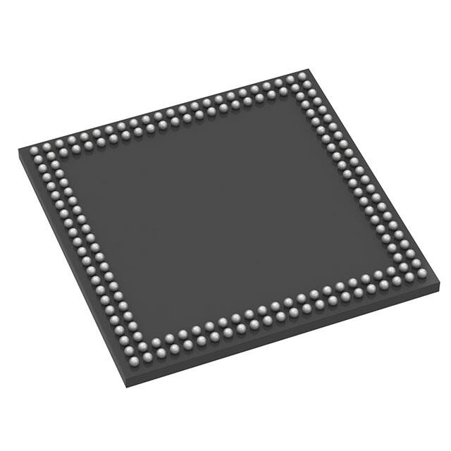


 工商网监
湘ICP备2023018690号
工商网监
湘ICP备2023018690号
