A S1110
1 General Description
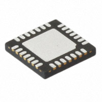
The AS1110 is designed to drive up to 16 LEDs through a fast serial interface and features 16 output constant current drivers and an on-chip diagnostic read-back function. The high clock-frequency (up to 50MHz), adjustable output current, and flexible serial interface makes the device perfectly suited for high-volume transmission applications. Output current is adjustable (up to 100mA/channel) using an external resistor (REXT). The serial interface with Schmitt trigger inputs includes an integrated shift register. Additionally, an internal data register stores the currently displayed data. The device features integrated diagnostics for overtemperature, open-LED, and shorted-LED conditions. Integrated registers store global fault status information during load as well as the detailed temperature/openLED/shorted-LED diagnostics results. The AS1110 also features a low-current diagnostic mode to minimize display flicker during fault testing. The AS1110 is available in a 24-pin SSOP and the 28pin QFN (5x5mm) package.
D a ta s h e e t
C o n s tan t - C u r r e n t , 1 6 - C h a n n e l L ED Driver with Diagnost ics
2 Key Features
! !
16 Constant-Current Output Channels Excellent Output Current Accuracy - Between Channels: 25mA
If multiple AS1110 devices are cascaded and tr or tf is large, it may be critical to achieve the timing required for data transfer between two cascaded LED drivers.
www.austriamicrosystems.com
Revision 1.04
6 - 24
�AS1110
Datasheet - Ty p i c a l O p e r a t i n g C h a r a c t e r i s t i c s
7 Typical Operating Characteristics
Figure 3. Output Current vs. REXT, VDD = 5V; VDS = 0.8V, TAMB = 25°C
100
Figure 4. Relative Output Current Error vs. VDD, Iout/Iout@VDD=5V - 1, TAMB = 25°C
2
Relative Output Current Error (%) .
1.5 1
REXT = 744Ω; VDS = 0.5V REXT = 186Ω; VDS = 0.8V
IOUT (mA) .
0.5 0
10
-0.5 -1
REXT = 372Ω; VDS = 0.6V
-1.5 -2 3 3.5 4 4.5 5 5.5
1 100
1000
10000
REXT (Ω)
VDD (V)
Figure 5. Output Current vs. VDS; VDD = 5V, TAMB = 25°C
120 100
REXT = 186Ω
Figure 6. Output Current vs. VDS; VDD = 5V, TAMB = 25°C
120 100
REXT = 186Ω
IOUT (mA) .
REXT = 251Ω
IOUT (mA) .
80 60
REXT = 372Ω
80
REXT = 251Ω
60 40 20 0
REXT = 372Ω
40 20 0 0 3 6 9 12 15
REXT = 744Ω
REXT = 744Ω
0
0.2
0.4
0.6
0.8
1
1.2
1.4
VDS (V)
VDS (V)
Figure 7. Output Current vs. VDD
120 100
VDS = 0.8V
IOUT (mA) .
80
VDS = 0.7V
60
VDS = 0.6V
40 20 0 3 3.5 4 4.5 5 5.5
VDS = 0.5V
VDD (V)
www.austriamicrosystems.com
Revision 1.04
7 - 24
�AS1110
Datasheet - D e t a i l e d D e s c r i p t i o n
8 Detailed Description
The AS1110 is designed to drive up to 16 LEDs through a fast serial interface and 16 constant-current output drivers. Furthermore, the AS1110 provides diagnostics for detecting open- or shorted-LEDs, as well as over-temperature conditions for LED display systems, especially LED traffic sign applications. The AS1110 contains an 16-bit shift register and an 16-bit data register, which convert serial input data into parallel output format. At AS1110 output stages, sixteen regulated current sinks are designed to provide uniform and constant current with excellent matching between ports for driving LEDs within a wide range of forward voltage variations. External output current is adjustable from 0.5 to 100mA using an external resistor for flexibility in controlling the brightness intensity of LEDs. The AS1110 guarantees to endure 15V maximum at the outputs. The serial interface is capable of operating at a minimum of 30 MHz, satisfying the requirements of high-volume data transmission. Using a multiplexed input/output technique, the AS1110 adds additional functionality to pins SDO, LD and OEN. These pins provide highly useful functions (open- and shorted-LED detection, over-temperature detection), thus reducing pin count. Over-temperature detection will work on-the-run, whereas the open- and shorted-LED detection can be used on-the-run or in low-current diagnostic mode (see page 15). Figure 8. Block Diagram
+VLED OUTN10 OUTN12 OUTN13 OUTN14 OUTN15 Global Error Detection OUTN11 OUTN0 OUTN1 OUTN2 OUTN3 OUTN4 OUTN5 OUTN6 OUTN7 OUTN8 OUTN9
REXT Current Generators OEN LD
Temperature Detection
16-Bit Open Detection & Error Register
16-Bit Short Detection & Error Register
AS1110
16-Bit Data Register
Detailed Error Detection
CLK SDI
16-Bit Shift Register Control Logic
SDO
Indicates 16 Bit Path
www.austriamicrosystems.com
Revision 1.04
8 - 24
�AS1110
Datasheet - D e t a i l e d D e s c r i p t i o n
Serial Interface
Data accesses are made serially via pins SDI and SDO. At each CLK rising edge, the signal present at pin SDI is shifted into the first bit of the internal shift register and the other bits are shifted ahead of the first bit. The MSB is the first bit to be clocked in. In error-detection mode the shift register will latch-in the corresponding error data of temperature-, open-, and short-error register with each falling edge of LD. The 16-bit data register will latch the data of the shift register at each rising edge of LD. This data is then used to drive the current generator output drivers to switch on the corresponding LEDs as OEN goes low.
Timing Diagrams
This section contains timing diagrams referenced in other sections of this data sheet. Figure 9. Normal Mode Timing Diagram
tW(CLK) CLK 50% 50% 50%
tSU(D) SDI 50%
tH(D) 50%
SDO
50% tP1
tW(L) LD 50% tSU(L) 50% tH(L)
OEN
OEN Low = Output Enabled OUTNx High = Output Off OUTNx Low = Output On
OUTNx
50%
tP2
Figure 10. Output Delay Timing Diagram
tW(OE) OEN 50% tP3 90% OUTN0 50% tOF tSTAG OUTN1 50% 10% 50% tP3 90% 10% tOR tSTAG 50% 50%
14XtSTAG OUTN15 50%
14XtSTAG 50%
www.austriamicrosystems.com
Revision 1.04
9 - 24
�AS1110
Datasheet - D e t a i l e d D e s c r i p t i o n
Figure 11. Data Input Timing Diagram
OEN tSU(L) tSU(OE)
tW(OE)
LD
16 CLK Pulses
tW(L)
CLK tSU(D) SDI0 Data Bit 15 Data Bit 14 Data Bit 13 Data Bit 12 Data Bit Data Bit n 2 Data Bit 1 Data Bit 0 tH(D) SDO0 Old Data Old Data Old Data Old Data Old Data Old Data Old Data Old Data Bit 15 Bit 14 Bit 13 Bit 12 Bit n Bit 2 Bit 1 Bit 0 tP1 Don’t Care Don’t Care
Figure 12. Data Input Example Timing Diagram
Time CLK SDI LD OEN OUTN0 OUTN1 OUTN2 OUTN3 OUTN4 OUTN5 OUTN6 OUTN7 OUTN8 OUTN9 OUTN10 OUTN11 OUTN12 OUTN13 OUTN14 OUTN15
1
2
3
4
5
6
7
8
9
10
11
12
13
14
15
D1 D14 D13 D12 D11 D10
D9
D8
D7
D6
D5
D4
D3
D2
D1
D0
Off On Off On Off On Off On Off On Off On Off On Off On Off On Off On Off On Off On Off On Off On Off On Off On
www.austriamicrosystems.com
Revision 1.04
10 - 24
�AS1110
Datasheet - D e t a i l e d D e s c r i p t i o n
Figure 13. Switching Global Error Mode Timing Diagram
OEN tTESTING tGSW(ERROR) tSU(ERROR) tP(I/O) tP(I/O) tP(I/O) tGSW(ERROR)
LD
CLK
tGSW(ERROR)
SDI
TFLAG(IN)
OFLAG(IN)
SFLAG(IN)
SDO
Don’t Care tP4
TFLAG
Don’t Care
OFLAG
Don’t Care
SFLAG
Acquisition of Error Status
tSW(ERROR)
tSW(ERROR)
Error-Detection Mode
Acquisition of the error status occurs at the rising edge of OEN. Error-detection mode is started on the rising edge of LD when OEN is high. The CLK signal must be low when entering error detection mode. Error detection for open- and shorted-LEDs can only be performed for LEDs that are switched on during test time. To switch between error-detection modes clock pulses are needed (see Table 5). Note: To test all LEDs, a test pattern that turns on all LEDs must be input to the AS1110.
Global Error Mode
Global error mode is entered when error-detection mode is started. Clock pulses during this period are used to select between temperature, open-LED, and shorted-LED tests, as well as low-current diagnostic mode and shutdown mode (see Table 5). In global error mode, an error flag (TFLAG, OFLAG, SFLAG) is delivered to pin SDO if any errors are encountered. Table 5. Global Error Mode Selections Clock Pulses Output Port 0 1 2 3 4 Don't Care Enabled Enabled Don't Care Don't Care Error-Detection Mode Over-Temperature Detection Open-LED Detection Shorted-LED Detection Low-Current Diagnostic Mode Shutdown Mode SDI = 1: Wakeup SDI = 0: Shutdown Global Error Flag/Shutdown Condition TFLAG = SDO = 1: No over-temperature warning. TFLAG = SDO = 0: Over-temperature warning. OFLAG = SDO = 1: No open-LED error. OFLAG = SDO = 0: Open-LED error. SFLAG = SDO = 1: No shorted-LED error. SFLAG = SDO = 0: Shorted-LED error.
Note: For a valid result SDI must be 1 for the first device.
www.austriamicrosystems.com
Revision 1.04
11 - 24
�AS1110
Datasheet - D e t a i l e d D e s c r i p t i o n
If there are multiple AS1110s in a chain, the error flag will be gated through all devices. To get a valid result at the end of the chain, a logic 1 must be applied to the SDI input of the first device of the chain. If one device produces an error this error will show up after n*tP(I/O) + tSW(ERROR) at pin SDO of the last device in the chain. This means it is not possible to identify which device in the chain produced the error. Therefore, if a global error occurs, the detailed error report can be run to identify which AS1110, or LED produced the error. Note: When no error has occurred, the detailed error report can be skipped, setting LD and subsequently OEN low.
Error Detection Functions
Open-LED Detection
The AS1110 open-LED detection is based on the comparison between VDS and VTHL. The open LED status is aquired at the rising edge of OEN and stored internally. While detecting open-LEDs the output port must be turned on. Open LED detection can be started with 1 clock pulse during error detection mode while the output port is turned on. Note: LEDs which are turned off at test time cannot be tested and will be shown as a logic 1 in the detailed error report. Table 6. Open LED Detection Modes Output Port State On On Effective Output Point Conditions VDS < VTHL VDS > VTHL Detected Open-LED Error Status Code 0 1 Meaning Open Circuit Normal
Shorted-LED
The AS1110 shorted-LED detection is based on the comparison between VDS and VTHH. The shortened LED status is aquired at the rising edge of OEN and stored internally. While detecting shorted-LEDs the output port must be turned on. Shorted-LED detection can be started with 2 clock pulses during error detection mode while the output port is turned on. For valid results, the voltage at OUTN0:OUTN15 must be lower then VTHH under low-current diagnostic mode operating conditions. This can be achieved by reducing the VLED voltage or by adding additional diodes, resistors or LED’s. Note: LEDs which are turned off at test time cannot be tested and will be shown as a logic 1 in the detailed error report. Table 7. Shorted LED Detection Modes Output Port State On On Effective Output Point Conditions VDS > VTHH VDS < VTHH Detected Shorted-LED Error Status Code 0 1 Meaning Short Circuit Normal
Overtemperature
Thermal protection for the AS1110 is provided by continuously monitoring the device’s core temperature. The overtemperature status is aquired at the rising edge of OEN and stored internally. Table 8. Overtemperature Modes Output Port State Don’t Care Don’t Care Effective Output Point Conditions Temperature > TOV1 Temperature < TOV1 Detected Overtemperature Status Code 0 1 Meaning Overtemperature Condition Normal
www.austriamicrosystems.com
Revision 1.04
12 - 24
�AS1110
Datasheet - D e t a i l e d D e s c r i p t i o n
Detailed Error Reports
The detailed error report can be read out after global error mode has been run. At the falling edge of LD, the detailed error report of the selected test is latched into the shift register and can be clocked out with n*16 clock cycles (n is the number of AS1110s in a chain) via pin SDO. At the same time new data can be written into the shift register, which is loaded on the next rising edge of pin LD. This pattern is shown at the output drivers, at the falling edge of OEN.
Detailed Temperature Warning Report
The detailed temperature warning report can be read out immediately after global error mode has been run. SDI must be 1 for the first device. Bit0 of the 16bit data word represents the temperature flag of the chip. Figure 14. Detailed Temperature Warning Report Timing Diagram
Global Flag Readout OEN tGSW(ERROR) LD t(SU)ERROR CLK tP4 tH(L) Detailed Error Report Readout
SDI
DBit15
DBit14 DBit13 DBit12
DBitn
DBit2
DBit1
DBit0
Don’t Care Don’t Care
New Data Input SDO tP4 For detailed timing information see Timing Diagrams on page 9. TFLAG Undefined Temperature Error Report Output
TBit0
tP1
Detailed Temperature Warning Report Example Consider a case where four AS1110s are cascaded in one chain. The detailed error report lists the temperatures for each device in the chain: IC1:[70°] IC2:[85°] IC3:[170°] IC4:[60°] In this case, IC3 is overheated and will generate a global error, and therefore 4*16 clock cycles are needed to write out the detailed temperature warning report, and optionally read in new data. The detailed temperature warning report would look like this: XXXXXXXXXXXXXXX1 XXXXXXXXXXXXXXX1 XXXXXXXXXXXXXXX0 XXXXXXXXXXXXXXX1 The 0 in the detailed temperature warning report indicates that IC3 is the device with the over-temperature condition. Note: In an actual report there are no spaces in the output.
www.austriamicrosystems.com
Revision 1.04
13 - 24
�AS1110
Datasheet - D e t a i l e d D e s c r i p t i o n
Detailed Open-LED Error Report
The detailed open-LED error report can be read out immediately after global error mode has been run. SDI must be 1 for the first device. Figure 15. Detailed Open-LED Error Report Timing Diagram
Global Flag Readout OEN tTESTING LD tSU(ERROR) tGSW(ERROR) CLK tGSW(ERROR)
Acquisition of Error Status
Detailed Error Report Readout
tH(L)
tP4
tGSW(ERROR)
SDI
tSW(ERROR)
DBit15
DBit14 DBit13 DBit12 DBitn
DBit2
DBit1
DBit0
Don’t Care
New Data Input TFlag tP4 OFlag
OBit15 OBit14 OBit13 OBit12 OBitn OBit2 OBit1 OBit0
SDO
Don’t Care
Open Error Report Output
tP1
For detailed timing information see Timing Diagrams on page 9.
Detailed Open-LED Error Report Example Consider a case where three AS1110s are cascaded in one chain. A 1 indicates a LED is on, a 0 indicates a LED is off, and an X indicates an open LED. The open-LED test is only applied to LEDs that are turned on. This test is used with a test pattern where all LEDs are on at test time. IC1:[1111111111111111] IC2:[111XX11111111X11] IC3:[1111111111111111] IC2 has three open LEDs switched on due to input. 3*16 clock cycles are needed to write the entire error code out. The detailed error report would look like this: Input Data: 1 1 1 1 1 1 1 1 1 1 1 1 1 1 1 1 LED Status: 1 1 1 1 1 1 1 1 1 1 1 1 1 1 1 1 Failure Code: 1 1 1 1 1 1 1 1 1 1 1 1 1 1 1 1 1111111111111111 1 1 1 XX1 1 1 1 1 1 1 1 X1 1 1110011111111011 1111111111111111 1111111111111111 1111111111111111
Comparing this report with the input data indicates that IC2 is the device with two open LEDs at position 4 and 5 and one open LED at position 14. For such a test it is recommended to enter low-current diagnostic mode first (see LowCurrent Diagnostic Mode on page 15) to reduce screen flickering. This test can be used also on-the-fly without using an all 1s test pattern (see Figure 19 on page 17). Note: In an actual report there are no spaces in the output. LEDs turned off during test time cannot be tested and will show a logic 1 in the detailed error report.
www.austriamicrosystems.com
Revision 1.04
14 - 24
�AS1110
Datasheet - D e t a i l e d D e s c r i p t i o n
Detailed Shorted-LED Error Report
The detailed shorted-LED error report can be read out immediately after global error mode has been run (see Global Error Mode on page 11). SDI must be 1 for the first device. Figure 16. Detailed Shorted-LED Error Report Timing Diagram
Global Flag Readout OEN tTESTING LD tSU(ERROR) tGSW(ERROR) CLK tGSW(ERROR)
Acquisition of Error Status
Detailed Error Report Readout
tH(L) tP4 tGSW(ERROR)
SDI
DBit15
DBit14 DBit13 DBit12
DBitn
DBit2
DBit1
DBit0
Don’t Care
tSW(ERROR)
New Data Input
SBit15 SBit14 SBit13 SBit12 SBitn SBit2 SBit1 SBit0
SDO
TFLAG OFLAG TFLAG
SFLAG
Don’t Care
tP4 For detailed timing information see Timing Diagrams on page 9.
Shorted-LED Error Report Output
tP1
Detailed Shorted-LED Error Report Example Consider a case where three AS1110s are cascaded in one chain. A 1 indicates a LED is on, a 0 indicates a LED is off, and an X indicates a shorted LED. This test is used on-the-fly. IC1:[11111XX111111111] IC2:[1111111111111111] IC3:[X100011111111111] IC1 has two shorted LEDs which are switched on, IC3 has one shorted LED switched off due to input. 3*16 clock cycles are needed to write the entire error code out. The detailed error report would look like this: Input Data: 1 1 1 1 1 1 1 1 1 1 1 1 1 1 1 1 LED Status: 1 1 1 1 1 X X 1 1 1 1 1 1 1 1 1 Failure Code: 1 1 1 1 1 0 0 1 1 1 1 1 1 1 1 1 1111111111111111 1111111111111111 1111111111111111 0100011111111111 X1 1 1 1 1 1 1 1 1 1 1 1 1 1 1 1111111111111111
Showing IC1 as the device with two shorted LEDs at position 6 and 7, and IC3 with one shorted LED at position 1. The shorted LED at position 1 of IC3 cannot be detected, since LEDs turned off at test time are not tested and will show a logic "1" at the detailed error report. To test all LEDs this test should be run with an all 1s test pattern. For a test with an all on test pattern, low-current diagnostic mode should be entered first to reduce on-screen flickering. Note: In an actual report there are no spaces in the output. LEDs turned off during test time cannot be tested and will show a logic 1 in the detailed error report.
Low-Current Diagnostic Mode
To run the open- or shorted-LED test, a test pattern must be used that will turn on each LED to be tested. This test pattern will cause a short flicker on the screen while the test is being performed. The low-current diagnostic mode can be initiated prior to running a detailed error report to reduce this on-screen flickering. Note: Normally, displays using such a diagnostic mode require additional cables, resistors, and other components to reduce the current. The AS1110 has this current-reduction capability built-in, thereby minimizing the number of external components required. Low-current diagnostic mode can be initiated via 3 clock pulses during error-detection mode. After the falling edge of LD, a test pattern displaying all 1s can be written to the shift register which will be used for the next error-detection test.
www.austriamicrosystems.com
Revision 1.04
15 - 24
�AS1110
Datasheet - D e t a i l e d D e s c r i p t i o n
On the next falling edge of OEN, current is reduced to ILC. With the next rising edge of OEN the current will immediately increase to normal levels and the detailed error report can be read out entering error-detection mode. Figure 17. Switching into Low-Current Diagnostic Mode Timing Diagram
Low-Current Diagnosis Mode OEN tTESTING LD tSU(ERROR) Load Internal all 1s Test Pattern (optional) tH(L)
tGSW(ERROR) CLK tGSW(ERROR) tSW(ERROR) SDI
SDO
TFLAG OFLAG SFLAG
Don’t Care
Re-entering Error Detection Mode (see Figure 15) (see Figure 16) Normal Operation Current
tP1 For detailed timing information see Timing Diagrams on page 9.
Shutdown Mode
The AS1110 features a shutdown mode which can be entered via 4 clock pulses during error-detection mode. To enable the shutdown mode a 0 must be placed at SDI after the rising edge of the 3rd clock pulse. To disable shutdown mode a 1 must be placed at SDI after the 3rd clock pulse. The shutdown/wakeup information will be latched through if multiple AS1110 devices are in a chain. At the rising edge of the 4th clock pulse the shutdown bit will be read out and the AS1110 will shutdown or wakeup. Note: In shutdown mode the supply current drops down to PD(MAX) where VDS = VLED - VF. In this case, the lowest possible supply voltage or a voltage reducer (VDROP) should be used. The voltage reducer allows VDS = (VLED -VF) - VDROP. Note: Resistors or zener diodes can be used as a voltage reducer as shown in Figure 23.
www.austriamicrosystems.com
Revision 1.04
19 - 24
�AS1110
Datasheet - A p p l i c a t i o n I n f o r m a t i o n
Figure 23. Voltage Reducer using Resistor (Left) and Zener Diode (Right)
Voltage Supply Voltage Supply
VLED VF
}
VDROP
VDROP
{
VF VDS
VLED
VDS
AS1110
AS1110
www.austriamicrosystems.com
Revision 1.04
20 - 24
�AS1110
Datasheet - P a c k a g e D r a w i n g s a n d M a r k i n g s
10 Package Drawings and Markings
The AS1110 is available in a 28-pin QFN (5x5mm) package and a 24-pin SSOP package. Figure 24. 28-pin QFN (5x5mm) Packagee
-A-
D
INDEX AREA (D/2 xE/2) 4
D2 D2/2
-B-
D/2
E/2
NXL
e
E2/2
aaa C 2x
-BSEE DETAIL B 2 1
6 SEE DETAIL B
-A-
aaa C 2x TOP VIEW
N N-1
INDEX AREA (D/2 xE/2)
NXb bbb ddd
5 CA B C
Datum A or B
4
BTM VIEW
L1
ccc C NX 0.08 C
A
A1
Terminal Tip ODD TERMINAL SIDE 5
Symbol A A1 A3 L L1 aaa bbb ccc ddd eee ggg
Min 0.70 0.00 0.45 0.03
Typ 0.75 0.02 0.20 REF 0.55 0.15 0.10 0.10 0.05 0.08 0.10
Max 0.80 0.05 0.65 0.15
Notes 1, 2 1, 2 1, 2 1, 2 1, 2 1, 2 1, 2 1, 2 1, 2 1, 2 1, 2
Symbol D BSC E BSC D2 E2 K b e N ND NE
Min
3.00 3.00 0.20 0.18
Typ 5.00 5.00 3.15 3.15 0.25 0.50 28 7 7
A3
e
SIDE VIEW
SEATING PLANE -C-
Max
3.25 3.25 0.30
Notes 1, 2 1, 2 1, 2 1, 2 1, 2 1, 2, 5 1, 2 1, 2, 5 1, 2, 5
Notes:Unilateral coplanarity zone applies to the exposed heat sink slug as well as the terminals. 1. 2. 3. 4. Dimensioning and tolerancing conform to ASME Y14.5M-1994. All dimensions are in millimeters; angles in degrees. N is the total number of terminals. The terminal #1 identifier and terminal numbering convention shall conform to JEDEC 95 SPP-012. Details of terminal #1 identifier are optional but must be located within the zone indicated. The terminal #1 identifier may be either a mold or marked feature. 5. Dimension b applies to metallized terminal and is measured between 0.15 and 0.30mm from terminal tip. If one end of the terminal has the optional radius, the b dimension should not be measured in that radius area. 6. Dimensions ND and NE refer to the number of terminals on each D and E side, respectively.
www.austriamicrosystems.com
Revision 1.04
E2
E
21 - 24
�AS1110
Datasheet - P a c k a g e D r a w i n g s a n d M a r k i n g s
Figure 25. 24-pin SSOP Package
Symbol A A1 A2 b C D E E1 e h L θ
Min Max 1.35 1.75 0.10 0.25 1.37 1.57 0.20 0.30 0.19 0.25 8.55 8.74 5.79 6.20 3.81 3.99 0.635 BSC 0.22 0.49 0.40 1.27 0º 8º
www.austriamicrosystems.com
Revision 1.04
22 - 24
�AS1110
Datasheet - O r d e r i n g I n f o r m a t i o n
11 Ordering Information
The device is available as the standard products shown in Table 9. Table 9. Ordering Information Type AS1110-BSSU AS1110-BSST AS1110-BQFR AS1110-BQFT Description Constant-Current, 16-Channel LED Driver with Diagnostics Constant-Current, 16-Channel LED Driver with Diagnostics Constant-Current, 16-Channel LED Driver with Diagnostics Constant-Current, 16-Channel LED Driver with Diagnostics Delivery Form Tubes Tape and Reel Tray Tape and Reel Package 24-pin SSOP 24-pin SSOP 28-pin QFN (5x5mm) 28-pin QFN (5x5mm)
All devices are RoHS compliant and free of halogene substances.
www.austriamicrosystems.com
Revision 1.04
23 - 24
�AS1110
Datasheet
Copyrights
Copyright © 1997-2009, austriamicrosystems AG, Schloss Premstaetten, 8141 Unterpremstaetten, Austria-Europe. Trademarks Registered ®. All rights reserved. The material herein may not be reproduced, adapted, merged, translated, stored, or used without the prior written consent of the copyright owner. All products and companies mentioned are trademarks or registered trademarks of their respective companies.
Disclaimer
Devices sold by austriamicrosystems AG are covered by the warranty and patent indemnification provisions appearing in its Term of Sale. austriamicrosystems AG makes no warranty, express, statutory, implied, or by description regarding the information set forth herein or regarding the freedom of the described devices from patent infringement. austriamicrosystems AG reserves the right to change specifications and prices at any time and without notice. Therefore, prior to designing this product into a system, it is necessary to check with austriamicrosystems AG for current information. This product is intended for use in normal commercial applications. Applications requiring extended temperature range, unusual environmental requirements, or high reliability applications, such as military, medical life-support or lifesustaining equipment are specifically not recommended without additional processing by austriamicrosystems AG for each application. For shipments of less than 100 parts the manufacturing flow might show deviations from the standard production flow, such as test flow or test location. The information furnished here by austriamicrosystems AG is believed to be correct and accurate. However, austriamicrosystems AG shall not be liable to recipient or any third party for any damages, including but not limited to personal injury, property damage, loss of profits, loss of use, interruption of business or indirect, special, incidental or consequential damages, of any kind, in connection with or arising out of the furnishing, performance or use of the technical data herein. No obligation or liability to recipient or any third party shall arise or flow out of austriamicrosystems AG rendering of technical or other services.
Contact Information
Headquarters austriamicrosystems AG Tobelbaderstrasse 30 A-8141 Unterpremstaetten - Graz, Austria Tel: +43 (0) 3136 500 0 Fax: +43 (0) 3136 525 01
For Sales Offices, Distributors and Representatives, please visit: http://www.austriamicrosystems.com/contact-us
www.austriamicrosystems.com
Revision 1.04
24 - 24
�


 工商网监
湘ICP备2023018690号
工商网监
湘ICP备2023018690号
