Datasheet
AS1330
4 M H z , L o w Vo l ta g e , D C - D C St e p - U p C o n v e r t e r
1 General Description
The AS1330 is a synchronous, low voltage, high efficiency DC-DC boost converter running at a constant frequency of 4MHz. This very high oscillator frequency allows the usage of a very a small and low profile inductor with only 470nH. This results in a board space requirement of only 43mm² for the complete solutions including all external components. AS1330 generates an output voltage between 1.8 and 3.3V from input voltages down to 0.6V. Therefore it is ideal for application powered by a single cell battery. AS1330 provides an output current of 150mA @ 3.3V from a single cell. To support high efficiency across the entire load range the AS1330 is equipped with a synchronous rectifier and features a power save mode for light loads. To avoid harmful deep discharge of the battery during shutdown the AS1330 is equipped with an output disconnect function. AS1330 can either monitor the battery voltage (Sense pin) or report the status of the output voltage (POK). The AS1330 is available in a TDFN (2x2mm) 8-pin package.
2 Key Features
! ! ! ! ! ! ! ! ! ! ! !
Input Voltage Range: 0.6V to 3.0V Adjustable Output Voltage Range: 1.8V to 3.3V Fixed Output Voltage: 1.8V, 3.0V 0.85V Low Start-Up Voltage 4MHz Fixed-Frequency 91% Efficiency Delivers 150mA @ 3.3V (from Single AA Cell) Automatic Powersave Operation for light Loads Output Disconnect during Shutdown Anti-Ringing Control minimizes EMI Power Okay and Sense pin TDFN (2x2mm) 8-pin Package
3 Applications
The AS1330 is ideal for space critical applications where ultra-small size is critical as in medical diagnostic equipment, hand-held instruments, digital cameras, MP3 players, GPS receivers, and PC or Memory cards. Figure 1. AS1330 - Typical Application Diagram
L1
SW AA Battery VIN C1
VOUT
VOUT 1.8V C2
AS1330-1.8
POK On Off EN GND SENSE FB
www.austriamicrosystems.com/DC-DC_Step-Up/AS1330
Revision 1.04
1 - 16
�AS1330
Datasheet - P i n A s s i g n m e n t s
4 Pin Assignments
Figure 2. Pin Assignments (Top View)
SENSE 1 FB 2 EN 3 POK 4
8 VIN 7 VOUT
AS1330
9
6 SW 5 GND
Pin Descriptions
Table 1. Pin Descriptions Pin Number 1 Pin Name SENSE Description Sense Input. Represents the input for the Power-OK behaviour. This input can be used to supervise the input or the output voltage via a resistor divider. If connected to GND the POK output is related to VOUT. Feedback Pin. Feedback input to the gm error amplifier. Connect a resistor divider tap to this pin. The output voltage can be adjusted from 1.8 to 3.3V by: VOUT = 0.8V[1 + (R1/R2)] If the fixed output voltage version ist used, connect this pin to VOUT. Active-High Enable Input. A logic LOW reduces the supply current to < 1µA. Connect to pin VIN for normal operation. Power-OK Output. Active-High, open-drain output indicates an out-of-regulation condition. Connect a 100kΩ pull-up resistor to pin OUT for logic levels. Leave this pin unconnected if the Power-OK feature is not used. Low Level: High Level: Signal and Power Ground. Provide a short, direct PCB path between this pin and the negative side of the output capacitor(s). Switch Pin. Connect an inductor between this pin and VIN. Keep the PCB trace lengths as short and wide as is practical to reduce EMI and voltage overshoot. If the inductor current falls to zero, or pin EN is low, an internal 100Ω anti-ringing switch is connected from this pin to VIN to minimize EMI. Note: An optional Schottky diode can be connected between this pin and VOUT. Output Voltage. Bias is derived from VOUT when VOUT exceeds VIN. PCB trace length from VOUT to the output filter capacitor(s) should be as short and wide as is practical. Input Voltage. The AS1330 gets its start-up bias from VIN unless VOUT exceeds VIN, in which case the bias is derived from VOUT. Thus, once started, operation is completely independent from VIN. Operation is only limited by the output power level and the internal series resistance of the supply. Exposed Pad. The exposed pad must be connected to GND. Ensure a good connection to the PCB to achieve optimal thermal performance.
2
FB
3
EN
4
POK
5
GND
6
SW
7
VOUT
8
VIN
9
www.austriamicrosystems.com/DC-DC_Step-Up/AS1330
Revision 1.04
2 - 16
�AS1330
Datasheet - A b s o l u t e M a x i m u m R a t i n g s
5 Absolute Maximum Ratings
Stresses beyond those listed in Table 2 may cause permanent damage to the device. These are stress ratings only, and functional operation of the device at these or any other conditions beyond those indicated in Section 6 Electrical Characteristics on page 4 is not implied. Exposure to absolute maximum rating conditions for extended periods may affect device reliability. Table 2. Absolute Maximum Ratings Parameter All Pins to GND Operating Temperature Range Storage Temperature Range Latch-Up ESD Min -0.3 -40 -65 -100 2 Max 5 +85 +125 100 Units V ºC ºC mA kV @85°C, JEDEC 78 HBM MIL-Std. 883E 3015.7 methods The reflow peak soldering temperature (body temperature) specified is in accordance with IPC/JEDEC J-STD020D “Moisture/Reflow Sensitivity Classification for Non-Hermetic Solid State Surface Mount Devices”. The lead finish for Pb-free leaded packages is matte tin (100% Sn). Notes
Package Body Temperature
+260
ºC
www.austriamicrosystems.com/DC-DC_Step-Up/AS1330
Revision 1.04
3 - 16
�AS1330
Datasheet - E l e c t r i c a l C h a r a c t e r i s t i c s
6 Electrical Characteristics
VIN = +1.2V, VOUT = +3.0V, VEN = +1.3V, L = 1µH, C1 = C2 = 10µF, TAMB = -40°C to +85ºC (unless otherwise specified). Typ values @ TAMB = +25ºC. Table 3. Electrical Characteristics Symbol Input Minimum Start-Up Voltage VIN Regulation VOUT Output Voltage Adjust Range Output Voltage Accuracy VFB IFB Feedback Voltage Feedback Input Current
2
Parameter
Conditions
Min
Typ
Max
Units
IOUT = 1mA IOUT = 1mA 0.6
0.85
0.9 3.0
V V
Operating Voltage Range
1
1.8 VOUT > VIN + 0.6V for adjustable VOUT only VFB = 0.8V -3 0.776 0.8 10
3.0 +3 0.824
V % V nA
Operating Current IQPWS IQSHDN IQ Switches ILKN ILKP RONNMOS RONPMOS INMOS NMOS Switch Leakage PMOS Switch Leakage
3
Quiescent Current (Powersave Operation) Quiescent Current (Shutdown) Quiescent Current (Active)
VOUT = 3.15V VEN = 0V in continuous mode
30 0.05 3
50 5
µA µA mA
VSW = 3.6V VSW = VOUT = 3.6V
0.1 0.1 0.25 0.35 650 80 3.2 87 4
5 5
µA µA Ω Ω mA %
NMOS Switch On Resistance PMOS Switch On Resistance NMOS Current Limit Maximum Duty Cycle
1
fSW Shutdown VENH VENL IEN Power-OK
5
Switching Frequency
4.8
MHz
EN Input High EN Input Low EN Input Current
4
no load no load
1.2 0.25 1 1.5
V V µA
POK Voltage Low POK Leakage Current Power-OK Threshold 1. 2. 3. 4. 5.
IPOK = 1mA VPOK = 3V, TAMB = 25ºC Monitor VIN, Falling Edge Monitor VOUT, Falling Edge 0.72 90
0.1 1
0.4 100 0.76
V nA V %
92.5
95
Guaranteed by design and verified in lab characterisation. External Schottky diode is mandatory for output voltages higher than 3V. VOUT is forced to 3.6V in production test. Internal pull-down resistor. The POK parameters are tested with proprietary test modes.
Note: All limits are guaranteed. The parameters with min and max values are guaranteed with production tests or SQC (Statistical Quality Control) methods. www.austriamicrosystems.com/DC-DC_Step-Up/AS1330 Revision 1.04 4 - 16
�AS1330
Datasheet - Ty p i c a l O p e r a t i n g C h a r a c t e r i s t i c s
7 Typical Operating Characteristics
VIN = 1.2V, VOUT = 1.8V, L = 1µH, C1 = C2 = 10µF, TAMB = +25ºC (unless otherwise specified); Figure 3. Efficiency vs. Output Current, VOUT = 1.8V
100 90 80 70 60 50
Vin = 1.0V
Figure 4. Efficiency vs. Input Voltage, VOUT = 1.8V
100 90 80 70 60 50
Iout = 1mA
Efficiency (%)
Efficiency (%)
40 30 0.1 1 10 100
Vin = 1.2V Vin = 1.5V
40 30
Iout = 10mA Iout = 50mA
1000
0.8 0.9 1.0 1.1 1.2 1.3 1.4 1.5 1.6 1.7 1.8
Output Current (mA) Figure 5. Efficiency vs. Output Current, VOUT = 3.0V
100 90 80 70 60 50
Vin = 1.0V
Input Voltage (V) Figure 6. Efficiency vs. Input Voltage, VOUT = 3.0V
100 90 80 70 60 50
Vin = 1.5V Vin = 2.0V
Efficiency (%)
Efficiency (%)
40 30 0.1 1 10 100
40 30
Iout Iout Iout Iout
= 1mA = 10mA = 50mA = 100mA
1000
0.8 1.0 1.2 1.4 1.6 1.8 2.0 2.2 2.4 2.6 2.8 3.0
Output Current (mA) Figure 7. Efficiency vs. IOUT, Coil Comparision
100 90 80 70 60 50 40 30 0.1 1 10 100 1000
821nH EPL2010 470nH LQH 1µH LQH 1µH EPL2010
Input Voltage (V) Figure 8. Efficiency vs. IOUT, Coil Comparision
100 90 80 70 60 50 40
1µH EPL2010 821nH EPL2010 1µH LQH
VIN = 1.0V VOUT = 1.8V
VIN = 1.5V VOUT = 3.0V
Efficiency (%)
Efficiency (%)
30 0.1 1 10 100 1000
Output Current (mA) www.austriamicrosystems.com/DC-DC_Step-Up/AS1330 Revision 1.04
Output Current (mA) 5 - 16
�AS1330
Datasheet - Ty p i c a l O p e r a t i n g C h a r a c t e r i s t i c s
Figure 9. IOUT vs. VIN; VOUT = 1.8V
300 250
Figure 10. IOUT vs. VIN; VOUT = 3.0V
700 600
Output Current (mA)
Output Current (mA)
470nH EPL2010 1µH LQH
200 150 100 50 0 0.7 0.8 0.9 1.0 1.1 1.2 1.3 1.4
500 400 300 200 100 0 0.7 0.9 1.1 1.3 1.5 1.7 1.9 2.1 2.3 2.5
470nH EPL2010 1µH LQH
Input Voltage (V)
Input Voltage (V)
Figure 11. Powersave Threshold vs. VIN
200
Vout = 3.0V
Figure 12. VOUT vs. VIN; IOUT = 1mA
4
175
Vout = 1.8V
3.5
Output Current (mA)
125 100 75 50 25 0 0.8 1.0 1.2 1.4 1.6 1.8 2.0 2.2 2.4
Output Voltage (V)
150
3 2.5 2 1.5 1
Vout = 1.8V
0.5 0 0.5 1.0 1.5 2.0
Vout = 2.5V Vout = 3.0V
2.5
3.0
Input Voltage (V)
Input Voltage (V)
Figure 13. Startup Voltage vs. Output Current
2.5 2.25 2 1.75 1.5 1.25 1 0.75 0.5 0.25 0 0 20 40 60 80 100
Vout = 1.8V Vout = 3.0V
Figure 14. Input Current vs. Input Voltage
10
Input Current (mA)
Input Voltage (V)
1
0.1
0.01 0.5 1.0 1.5 2.0 2.5 3.0
Output Current (mA)
Input Voltage (V)
www.austriamicrosystems.com/DC-DC_Step-Up/AS1330
Revision 1.04
6 - 16
�AS1330
Datasheet - Ty p i c a l O p e r a t i n g C h a r a c t e r i s t i c s
Figure 15. Startup, VOUT = 3V, IOUT = 1mA
Figure 16. Shutdown, VOUT = 3V, IOUT = 1mA
1V/Div
VOUT
VOUT
100µs/Div
1V/Div
1ms/Div
Figure 17. Load Transient, VOUT = 3V
Figure 18. Load Transient, VOUT = 3V
100mV/Div
10mA
100µs/Div
100µs/Div
www.austriamicrosystems.com/DC-DC_Step-Up/AS1330
Revision 1.04
50mV/Div
VOUT
VOUT
50mA 100mA
IOUT
100mA
IOUT
1V/Div
1V/Div
EN
EN
7 - 16
�AS1330
Datasheet - D e t a i l e d D e s c r i p t i o n
8 Detailed Description
The AS1330 can operate from a single-cell input voltage (VIN) below 1V, and features fixed frequency (4MHz) and current mode PWM control for exceptional line- and load-regulation. With low RDS(ON) and gate charge internal NMOS and PMOS switches, the device maintains high-efficiency from light to heavy loads. Modern portable devices frequently spend extended time in low-power or standby modes, switching to high powerdrain only when certain functions are enabled. The AS1330 is ideal for portable devices since it maintain high-power conversion efficiency over a wide output power range, thus increasing battery life in these types of devices. In addition to high-efficiency at moderate and heavy loads, the AS1330 includes an automatic powersave mode that improves efficiency of the power converter at light loads. The powersave mode is initiated if the output load current falls below a factory programmed threshold.
Figure 19. AS1330 - Block Diagram
L1 1µH AA Battery C1 4.7µF
6 Start Up OSC
1
SW
– VOUT Good + 1.65V 5 VOUT 1.8V Output
VIN
A B
A/B MUX
PWM Control Sync Drive Control 4MHz Ramp Generator + PWM – Comp – Slope Compensator Σ
0.25Ω Current Sense
0.35Ω
AS1330
– gm Error Amp + 3
FB C2 4.7µF
0.8V Ref
On Off
4
EN
Shutdown Control
Shutdown
Powersave Operation Control
RC CC CP2
Powersave
1
SENSE
Sense & POK Logic
4
POK
2
GND
Low-Voltage Start-Up
The AS1330 requires VIN of only 0.85V (typ) or higher to start up. The low-voltage start-up circuitry controls the internal NMOS switch up to a maximum peak inductor current of 650mA (typ), with 1.5ms (approx.) off-time during start-up, allowing the devices to start up into an output load. With a VOUT > 1.65V, the start-up circuitry is disabled and normal fixed-frequency PWM operation is initiated. In this mode, the AS1330 operates independent of VIN, allowing extended operating time as the battery can drop to several tenths of a volt without affecting output regulation. The limiting factor for the application is the ability of the battery to supply sufficient energy to the output.
www.austriamicrosystems.com/DC-DC_Step-Up/AS1330
Revision 1.04
8 - 16
�AS1330
Datasheet - D e t a i l e d D e s c r i p t i o n
Low-Noise Fixed-Frequency Operation
Oscillator
The AS1330 switching frequency is internally fixed at 4MHz allowing the use of very small external components.
Current Sensing
A signal representing the internal NMOS-switch current is summed with the slope compensator. The summed signal is compared to the error amplifier output to provide a peak current control command for the PWM. Peak switch current is limited to approximately 650mA independent of VIN or VOUT.
Zero Current Comparator
The zero current comparator monitors the inductor current to the output and shuts off the PMOS synchronous rectifier once this current drops to 20mA (approx.). This prevents the inductor current from reversing polarity and results in improved converter efficiency at light loads.
Anti-Ringing Control
Anti-ringing control circuitry prevents high-frequency ringing on pin SW as the inductor current approaches zero. This is accomplished by damping the resonant circuit formed by the inductor and the capacitance on pin SW (CSW).
Powersave Operation
In light load conditions, the integrated powersave feature removes power from all circuitry not required to monitor VOUT. When VOUT has dropped approximately 1% from nominal, the device powers up and begins normal PWM operation. C2 recharges, causing the AS1330 to re-enter powersave mode as long as the output load remains below the powersave threshold. The frequency of this intermittent PWM is proportional to load current; i.e., as the load current drops further below the powersave threshold, the AS1330 turns on less frequently. When the load current increases above the powersave threshold, the AS1330 will resume continuous, seamless PWM operation.
Notes:
1. An optional capacitor (CFF) between pins VOUT and FB in some applications can reduce VOUTp-p ripple and input quiescent current during powersave mode. Typical values for CFF range from 15 to 220pF. 2. In powersave mode the AS1330 draws only 30µA from the output capacitor(s), greatly improving converter efficiency.
Shutdown
When pin EN is low the AS1330 is switched off and 850mA current rating and low DCR is recommended. For applications where radiated noise is a concern, a toroidal or shielded inductor can be used.
Capacitor Selection
A 4.7µF capacitor is recommended for C1 and for C2. Small-sized ceramic capacitors are recommended. X5R and X7R ceramic capacitors are recommended as they retain capacitance over wide ranges of voltages and temperatures.
Output Capacitor Selection
Low ESR capacitors should be used to minimize VOUT ripple. Multi-layer ceramic capacitors are recommended since they have extremely low ESR and are available in small footprints. Up to 10µF output capacitor is sufficient for most applications. Larger values up to 22µF may be used to obtain extremely low output voltage ripple and improve transient response. An additional phase lead capacitor may be required with output capacitors larger than 10µF to maintain acceptable phase margin. X5R and X7R dielectric materials are recommended due to their ability to maintain capacitance over wide voltage and temperature ranges.
Input Capacitor Selection
Low ESR input capacitors reduce input switching noise and reduce the peak current drawn from the battery. Ceramic capacitors are recommended for input decoupling and should be located as close to the device as is practical. A 4.7µF input capacitor is sufficient for most applications. Larger values may be used without limitations.
Table 4. Recommended External Components Name Part Number Value Rating Type Size Manufacturer Murata www.murata.com
C1, C2
GRM219R60J106KE19 GRM188R60J475KE19 LQH32PN1R0NN0 LQH32PNR47NN0
10µF 4.7µF 1µH 470nH 1µH 820nH 470nH
6.3V 6.3V 2.05A 2.55A 1.35A 1.6A 2.2A
X5R X5R 45mΩ 30mΩ 99mΩ 68mΩ 40mΩ
0805 0603 3.2x2.5x1.55mm 3.2x2.5x1.55mm
L1
EPL2010-102ML EPL2010-821ML EPL2010-471ML
2.0x2.0x1.0mm Coilcraft www.coilcraft.com 2.0x2.0x1.0mm 2.0x2.0x1.0mm
Diode Selection
A Schottky diode should be used to carry the output current for the time it takes the PMOS synchronous rectifier to switch on. For VOUT > 3.0V a schottky diode is mandatory, for VOUT ≤ 3.0V a it is optional, although using one will increase device efficiency by 2 to 3%. On one hand the schottky diode reduces the overshoot on the output signal but on the other hand the output disconnect function is no longer working.
Note: Do not use ordinary rectifier diodes, since the slow recovery times will compromise efficiency.
www.austriamicrosystems.com/DC-DC_Step-Up/AS1330
Revision 1.04
13 - 16
�AS1330
Datasheet - P a c k a g e D r a w i n g s a n d M a r k i n g s
10 Package Drawings and Markings
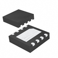
The device is available in a TDFN (2x2mm) 8-pin package.
Figure 24. TDFN (2x2mm) 8-pin package Diagram
Table 5. TDFN (2x2mm) 8-pin package Dimensions Symbol Min Typ Max A 0.51 0.55 0.60 A1 0.00 0.02 0.05 A3 0.15 ref aaa 0.15 bbb 0.10 ccc 0.10 k 0.20 b 0.20 0.25 0.30 e 0.50 Note:
Symbol D E D2 E2 L N ND NE
Min
1.45 0.75 0.225
Typ 2.00 2.00 1.60 0.90 0.325 8 4 --
Max
1.70 1.00 0.425
3. Dimensioning and tolerancing conform to ASME Y14.5M-1994. 4. All dimensions are in millimeters, angle is in degrees. 5. Terminal #1 identifier and terminal numbering convention shall conform to JESD 95-1 SPP-012. Details of terminal #1 identifier are optional, but must be located within the area indicated. The terminal #1 identifier may be either a mold, embedded metal or mark feature. 6. Dimension b applies to metallized terminal and is measured between 0.15 and 0.30mm from terminal tip.
www.austriamicrosystems.com/DC-DC_Step-Up/AS1330
Revision 1.04
14 - 16
�AS1330
Datasheet - O r d e r i n g I n f o r m a t i o n
11 Ordering Information
The device is available as the standard products listed in Table 6.
Table 6. Ordering Information Ordering Code Marking Output Descriptiom Delivery Form
AS1330-BTDT-AD AS1330-BTDT-18 AS1330-BTDT-30
AV AU AZ
adjustable 4MHz, Low Voltage, DC-DC StepUp Converter 1.8V 3.0V 4MHz, Low Voltage, DC-DC StepUp Converter 4MHz, Low Voltage, DC-DC StepUp Converter
Tape and Reel Tape and Reel Tape and Reel
Package TDFN (2x2mm) 8-pin
TDFN (2x2mm) 8-pin TDFN (2x2mm) 8-pin
Note: All products are RoHS compliant and Pb-free. Buy our products or get free samples online at ICdirect: http://www.austriamicrosystems.com/ICdirect
For further information and requests, please contact us mailto:sales@austriamicrosystems.com or find your local distributor at http://www.austriamicrosystems.com/distributor
www.austriamicrosystems.com/DC-DC_Step-Up/AS1330
Revision 1.04
15 - 16
�AS1330
Datasheet
Copyrights
Copyright © 1997-2010, austriamicrosystems AG, Tobelbaderstrasse 30, 8141 Unterpremstaetten, Austria-Europe. Trademarks Registered ®. All rights reserved. The material herein may not be reproduced, adapted, merged, translated, stored, or used without the prior written consent of the copyright owner. All products and companies mentioned are trademarks or registered trademarks of their respective companies.
Disclaimer
Devices sold by austriamicrosystems AG are covered by the warranty and patent indemnification provisions appearing in its Term of Sale. austriamicrosystems AG makes no warranty, express, statutory, implied, or by description regarding the information set forth herein or regarding the freedom of the described devices from patent infringement. austriamicrosystems AG reserves the right to change specifications and prices at any time and without notice. Therefore, prior to designing this product into a system, it is necessary to check with austriamicrosystems AG for current information. This product is intended for use in normal commercial applications. Applications requiring extended temperature range, unusual environmental requirements, or high reliability applications, such as military, medical life-support or life-sustaining equipment are specifically not recommended without additional processing by austriamicrosystems AG for each application. For shipments of less than 100 parts the manufacturing flow might show deviations from the standard production flow, such as test flow or test location. The information furnished here by austriamicrosystems AG is believed to be correct and accurate. However, austriamicrosystems AG shall not be liable to recipient or any third party for any damages, including but not limited to personal injury, property damage, loss of profits, loss of use, interruption of business or indirect, special, incidental or consequential damages, of any kind, in connection with or arising out of the furnishing, performance or use of the technical data herein. No obligation or liability to recipient or any third party shall arise or flow out of austriamicrosystems AG rendering of technical or other services.
Contact Information
Headquarters austriamicrosystems AG Tobelbaderstrasse 30 A-8141 Unterpremstaetten, Austria Tel: +43 (0) 3136 500 0 Fax: +43 (0) 3136 525 01 For Sales Offices, Distributors and Representatives, please visit: http://www.austriamicrosystems.com/contact
www.austriamicrosystems.com/DC-DC_Step-Up/AS1330
Revision 1.04
16 - 16
�


 工商网监
湘ICP备2023018690号
工商网监
湘ICP备2023018690号
