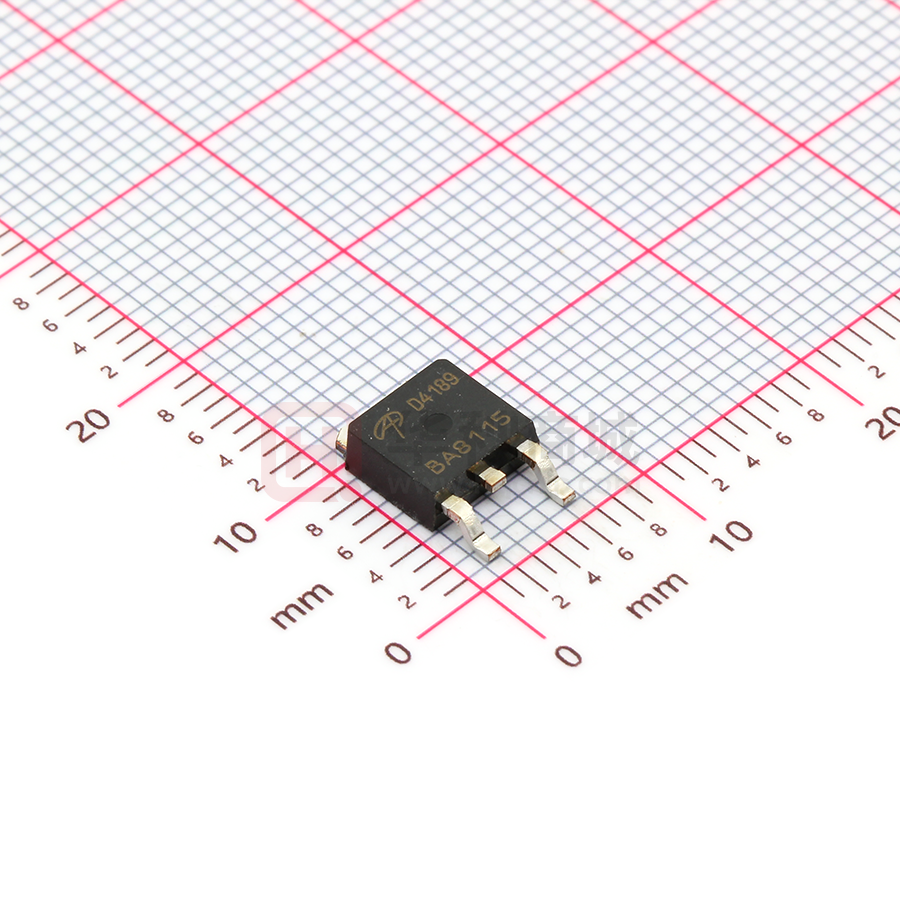
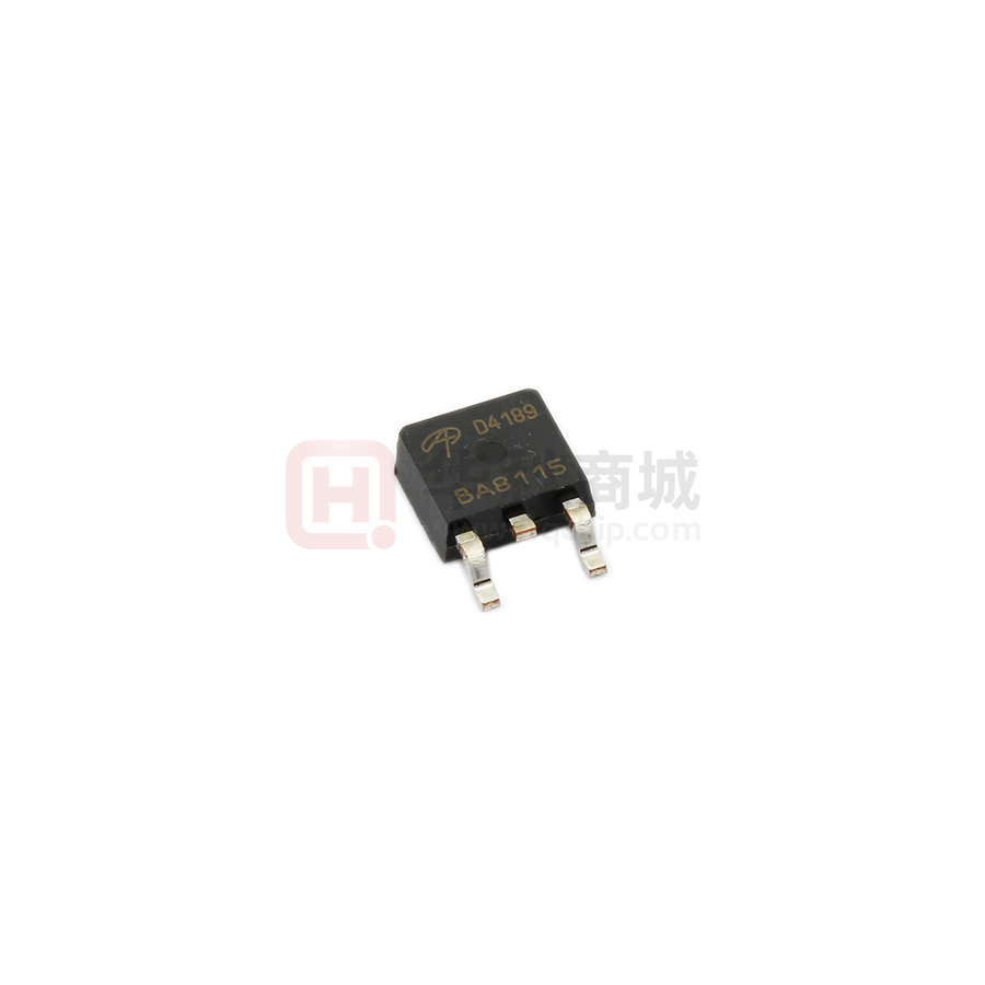
AOD4189 P-Channel Enhancement Mode Field Effect Transistor
General Description
The AOD4189 uses advanced trench technology and design to provide excellent RDS(ON) with low gate charge. With the excellent thermal resistance of the DPAK package, this device is well suited for high current load applications. -RoHS Compliant -Halogen Free*
TO-252 D-PAK
Features
VDS (V) = -40V ID = -40A (V GS = -10V) RDS(ON) < 22mΩ (VGS = -10V) RDS(ON) < 29mΩ (VGS = -4.5V) 100% UIS Tested! 100% Rg Tested!
Top View D
Bottom View
D
G S G S G S
Absolute Maximum Ratings TC=25°C unless otherwise noted Parameter Symbol VDS Drain-Source Voltage Gate-Source Voltage Continuous Drain Current B,H Pulsed Drain Current Avalanche Current
C C C
Maximum -40 ±20 -40 -28 -50 -35 61 62.5 31 2.5 1.6 -55 to 175
Units V V
VGS TC=25°C TC=100°C ID IDM IAR EAR PD PDSM TJ, TSTG
A
Repetitive avalanche energy L=0.1mH TC=25°C Power Dissipation B Power Dissipation
A
mJ
TC=100°C TA=25°C TA=70°C
W
Junction and Storage Temperature Range Thermal Characteristics Parameter A,G Maximum Junction-to-Ambient A,G Maximum Junction-to-Ambient Maximum Junction-to-Case D,F
°C
Symbol t ≤ 10s Steady-State Steady-State RθJA RθJC
Typ 15 41 2
Max 20 50 2.4
Units °C/W °C/W °C/W
Alpha & Omega Semiconductor, Ltd.
www.aosmd.com
�AOD4189
Electrical Characteristics (TJ=25°C unless otherwise noted) Parameter Symbol STATIC PARAMETERS Drain-Source Breakdown Voltage BVDSS IDSS IGSS VGS(th) ID(ON) RDS(ON) gFS VSD IS Zero Gate Voltage Drain Current Gate-Body leakage current Gate Threshold Voltage On state drain current Static Drain-Source On-Resistance VGS=-4.5V, ID=-8A Forward Transconductance Diode Forward Voltage VDS=-5V, ID=-12A IS=-1A,VGS=0V Conditions ID=-250µA, VGS=0V VDS=-40V, VGS=0V TJ=55°C VDS=0V, VGS= ±20V VDS=VGS ID=-250µA VGS=-10V, VDS=-5V VGS=-10V, ID=-12A TJ=125°C -1.7 -50 18 27 23 35 -0.74 -1 -20 1870 VGS=0V, VDS=-20V, f=1MHz VGS=0V, VDS=0V, f=1MHz 2.5 185 155 4.5 31.4 VGS=-10V, VDS=-20V, ID=-12A 7.9 7.6 6.2 10 VGS=-10V, VDS=-20V, RL=1.6Ω, RGEN=3Ω IF=-12A, dI/dt=100A/µs 18 38 24 32 30 42 6.5 41 10 nC nC ns ns ns ns ns nC 22 33 29 S V A pF pF pF Ω nC mΩ -1.9 Min -40 -1 -5 ±100 -3 Typ Max Units V µA nA V A
Maximum Body-Diode Continuous Current
DYNAMIC PARAMETERS Input Capacitance Ciss Coss Crss Rg Output Capacitance Reverse Transfer Capacitance Gate resistance
SWITCHING PARAMETERS Qg (-10V) Total Gate Charge Qg (-4.5V) Total Gate Charge Qgs Qgd tD(on) tr tD(off) tf trr Qrr Gate Source Charge Gate Drain Charge Turn-On DelayTime Turn-On Rise Time Turn-Off DelayTime Turn-Off Fall Time Body Diode Reverse Recovery Time Body Diode Reverse Recovery Charge IF=-12A, dI/dt=100A/µs
A: The value of R θJA is measured with the device in a still air environment with T A =25°C. The power dissipation P DSM and current rating IDSM are based on T J(MAX)=150°C, using steady state junction-to-ambient thermal resistance. B. The power dissipation P D is based on T J(MAX)=175°C, using junction-to-case thermal resistance, and is more useful in setting the upper dissipation limit for cases where additional heatsinking is used. C: Repetitive rating, pulse width limited by junction temperature T J(MAX)=175°C. D. The RθJA is the sum of the thermal impedence from junction to case R θJC and case to ambient. E. The static characteristics in Figures 1 to 6 are obtained using t ≤300 µs pulses, duty cycle 0.5% max. F. These curves are based on the junction-to-case thermal impedence which is measured with the device TBD mounted to a large heatsink, assuming a maximum junction temperature of T J(MAX)=175°C. The SOA curve provides a single pulse rating. TBD G. These tests are performed with the device mounted on 1 in 2 FR-4 board with 2oz. Copper, in a still air environment with T A=25°C. H. The maximum current rating is limited by bond-wires. *This device is guaranteed green after data code 8X11 (Sep 1 ST 2008). Rev1: Oct 2008 COMPONENTS IN LIFE SUPPORT DEVICES OR SYSTEMS ARE NOT AUTHORIZED. AOS DOES NOT ASSUME ANY LIABILITY ARISING OUT OF SUCH APPLICATIONS OR USES OF ITS PRODUCTS. AOS RESERVES THE RIGHT TO IMPROVE PRODUCT DESIGN, FUNCTIONS AND RELIABILITY WITHOUT NOTICE.
Alpha & Omega Semiconductor, Ltd.
www.aosmd.com
�AOD4189
TYPICAL ELECTRICAL AND THERMAL CHARACTERISTICS
50 -10V 40 -6.0V -ID (A) VGS=-3.5V 20 -ID(A) 30 30 20 -4.5V -4.0V 40 50 VDS=-5V
10 0 0 1 2 3 4 5 -VDS (Volts) Figure 1: On-Region Characteristics
10
125°C 25°C
0 1.5 2 2.5 3 3.5 4 4.5 -VGS(Volts) Figure 2: Transfer Characteristics
30 Normalized On-Resistance 28 26 RDS(ON) (mΩ ) 24 22 20 18 16 0 10 20 30 40 -ID (A) Figure 3: On-Resistance vs. Drain Current and Gate Voltage VGS=-10V VGS=-4.5V
2 1.8 1.6 1.4 1.2 1 0.8 -50 -25 0 25 50 75 100 125 150 175 200 Temperature (°C) Figure 4: On-Resistance vs. Junction Temperature 100 ID=-12A VGS=-4.5V ID=-8A VGS=-10V ID=-12A
55 50 45 RDS(ON) (mΩ ) -IS (A) 40 35 30 125°C
150
10 1 0.1 0.01 0.001 125°C 25°C
mJ
25 20 15 3 4 5 6 7
25°C
0.0001 0.00001 8 9 10 0.0 0.2 0.4 0.6 0.8 1.0 1.2 -VSD (Volts) Figure 6: Body-Diode Characteristics
-VGS (Volts) Figure 5: On-Resistance vs. Gate-Source Voltage
Alpha & Omega Semiconductor, Ltd.
www.aosmd.com
�AOD4189
TYPICAL ELECTRICAL AND THERMAL CHARACTERISTICS
10 VDS=-20V ID=-12A Capacitance (pF) 2800 2400 Ciss 2000 1600 1200 800 Crss 400 0 0 5 10 15 20 25 30 35 Qg (nC) Figure 7: Gate-Charge Characteristics 0 0 5 10 15 20 25 30 35 40 -VDS (Volts) Figure 8: Capacitance Characteristics Coss
8 -VGS (Volts)
6
4
2
100 10µs Power (W) -ID (Amps) 100µs 10 RDS(ON) limited 1ms TJ(Max)=175°C TC=25°C 1 1 10 -VDS (Volts) Figure 9: Maximum Forward Biased Safe Operating Area (Note F) 100 10ms DC
10000 TJ(Max)=175°C TC=25°C 1000
100
10 0.00001
0.0001
0.001
0.01
0.1
1
Pulse Width (s) Figure 10: Single Pulse Power Rating Junction-toCase (Note F)
10 Zθ Jc Normalized Transient Thermal Resistance
D=Ton/T TJ,PK=Tc+PDM.ZθJC.RθJC RθJC=2.4°C/W
In descending order D=0.5, 0.3, 0.1, 0.05, 0.02, 0.01, single pulse
150
mJ
1
0.1
PD Ton Single Pulse
T 0.1 1
0.01 0.00001
0.0001
0.001
0.01
Pulse Width (s) Figure 11: Normalized Maximum Transient Thermal Impedance (Note F)
Alpha & Omega Semiconductor, Ltd.
www.aosmd.com
�AOD4189
TYPICAL ELECTRICAL AND THERMAL CHARACTERISTICS
100 -IA, Peak Avalanche Current (A)
70
60
Power Dissipation (W) 0.1 1 10 100 1000
50
10
40
30
20
10
1 0.01
0 0 25 50 75 100 125 150 175 TCASE (°C) Figure 13: Power De-rating (Note B)
Time in Avalache, t A (s) Figure 12: Single Pulse Avalanche Capability
50 40 30 20 10 0 0 25 50 75 100 125 150 175
10000
TJ(Max)=150°C TA=25°C
Current rating -ID (A)
1000 Power (W)
100
10
1 1E-04 0.001
TCASE (°C) Figure 14: Current De-rating (Note B)
0.1 1 10 100 1000 Pulse Width (s) Figure 15: Single Pulse Power Rating Junctionto-Ambient (Note G)
0.01
10 Zθ JA Normalized Transient Thermal Resistance D=Ton/T TJ,PK=TA+PDM.ZθJA.RθJA RθJA=50°C/W
150 In descending order D=0.5, 0.3, 0.1, 0.05, 0.02, 0.01, single pulse
1
0.1 PD 0.01 Ton Single Pulse 0.001 0.00001 0.0001 0.001 0.01 0.1 1 10 T 100 1000
Pulse Width (s) Figure 16: Normalized Maximum Transient Thermal Impedance (Note G)
Alpha & Omega Semiconductor, Ltd.
www.aosmd.com
�AOD4189
Gate Charge Test Circuit & Waveform
Vgs Qg -10V
VDC
VDC
DUT Vgs Ig
Resistive Switching Test Circuit & Waveforms
RL Vds Vgs Vgs Rg DUT
VDC
Vgs Vds
Unclamped Inductive Switching (UIS) Test Circuit & Waveforms
L Vds Id Vgs Rg DUT Vgs Vgs Vgs
VDC
Diode Recovery Test Circuit & Waveforms
Vds + DUT Vgs
t rr
Vds -
Isd Vgs
L
VDC
+ Vdd -Vds
Ig
Alpha & Omega Semiconductor, Ltd.
+
-
+
-
+
Charge
ton td(on) tr td(off) toff tf
-
+
-
Vds
Qgs
Qgd
Vdd
90%
10%
EAR= 1/2 LIAR
2
Vds BVDSS Vdd Id I AR
Q rr = - Idt
-Isd
-I F
dI/dt -I RM Vdd
www.aosmd.com
�


 工商网监
湘ICP备2023018690号
工商网监
湘ICP备2023018690号