AON7405
30V P-Channel MOSFET
General Description
Product Summary
The AON7405 uses advanced trench technology to
provide excellent RDS(ON) with low gate charge.
This device is ideal for load switch and battery protection
applications.
ID (at VGS= -10V)
-30V
-50A
RDS(ON) (at VGS= -10V)
< 6.2mΩ
RDS(ON) (at VGS = -6V)
< 8.9mΩ
VDS
• RoHS and Halogen-Free Compliant
100% UIS Tested
100% Rg Tested
D
Top View
DFN 3.3x3.3 EP
Top View
Bottom
Pin 1
1
8
2
7
3
6
4
5
G
S
Absolute Maximum Ratings TA=25°C unless otherwise noted
Parameter
Symbol
Drain-Source Voltage
VDS
Gate-Source Voltage
VGS
TC=25°C
Continuous Drain
CurrentG
Pulsed Drain Current
Continuous Drain
Current
V
-39
A
-25
IDSM
TA=70°C
±25
-210
IDM
TA=25°C
Units
V
-50
ID
TC=100°C
C
Maximum
-30
A
-20
Avalanche Current C
IAR, IAS
-44
A
Repetitive avalanche energy L=0.1mH C
TC=25°C
EAR, EAS
97
mJ
Power Dissipation B
TC=100°C
TA=25°C
Power Dissipation A
Junction and Storage Temperature Range
Rev.2. 0: May 2013
6.25
Steady-State
Steady-State
RθJA
RθJC
www.aosmd.com
W
4
TJ, TSTG
Symbol
t ≤ 10s
W
33
PDSM
TA=70°C
Thermal Characteristics
Parameter
Maximum Junction-to-Ambient A
Maximum Junction-to-Ambient A D
Maximum Junction-to-Case
83
PD
-55 to 150
Typ
16
45
1.1
°C
Max
20
55
1.5
Units
°C/W
°C/W
°C/W
Page 1 of 6
�AON7405
Electrical Characteristics (TJ=25°C unless otherwise noted)
Symbol
Parameter
STATIC PARAMETERS
BVDSS
Drain-Source Breakdown Voltage
IDSS
Zero Gate Voltage Drain Current
Conditions
Min
ID=-250µA, VGS=0V
-30
-1
TJ=55°C
-5
Gate-Body leakage current
VDS=0V, VGS= ±25V
VGS(th)
Gate Threshold Voltage
VDS=VGS ID=-250µA
-1.7
ID(ON)
On state drain current
VGS=-10V, VDS=-5V
-210
µA
±100
nA
-2.8
V
5.1
6.2
7.6
9.2
VGS=-6V, ID=-20A
7.1
8.9
VGS=-4.5V, ID=-10A
10.7
TJ=125°C
gFS
Forward Transconductance
VDS=-5V, ID=-20A
VSD
Diode Forward Voltage
IS=-1A,VGS=0V
IS
Units
-2.2
VGS=-10V, ID=-20A
Static Drain-Source On-Resistance
Max
V
VDS=-30V, VGS=0V
IGSS
RDS(ON)
Typ
Maximum Body-Diode Continuous Current
A
G
DYNAMIC PARAMETERS
Ciss
Input Capacitance
mΩ
mΩ
46
-0.7
mΩ
S
-1
V
-50
A
1960
2450
2940
pF
380
550
720
pF
220
370
520
pF
7
14
28
Ω
SWITCHING PARAMETERS
Qg(10V) Total Gate Charge
33
42
51
nC
Qg(4.5V) Total Gate Charge
16
21
26
nC
5.5
7
8.5
nC
12
17
nC
Coss
Output Capacitance
Crss
Reverse Transfer Capacitance
Rg
Gate resistance
Qgs
Gate Source Charge
Qgd
Gate Drain Charge
tD(on)
Turn-On DelayTime
tr
Turn-On Rise Time
tD(off)
Turn-Off DelayTime
tf
Turn-Off Fall Time
VGS=0V, VDS=-15V, f=1MHz
VGS=0V, VDS=0V, f=1MHz
VGS=-10V, VDS=-15V, ID=-20A
7
VGS=-10V, VDS=-15V,
RL=0.75Ω, RGEN=3Ω
9.5
ns
10
ns
104
ns
78
ns
trr
Body Diode Reverse Recovery Time
IF=-20A, dI/dt=500A/µs
20
25
30
Qrr
Body Diode Reverse Recovery Charge IF=-20A, dI/dt=500A/µs
37
47
57
ns
nC
A. The value of RθJA is measured with the device mounted on 1in2 FR-4 board with 2oz. Copper, in a still air environment with TA =25°C. The
Power dissipation PDSM is based on R θJA t ≤ 10s value and the maximum allowed junction temperature of 150°C. The value in any given
application depends on the user's specific board design.
B. The power dissipation PD is based on TJ(MAX)=150°C, using junction-to-case thermal resistance, and is more useful in setting the upper
dissipation limit for cases where additional heatsinking is used.
C. Repetitive rating, pulse width limited by junction temperature TJ(MAX)=150°C. Ratings are based on low frequency and duty cycles to keep
initial TJ =25°C.
D. The RθJA is the sum of the thermal impedence from junction to case RθJC and case to ambient.
E. The static characteristics in Figures 1 to 6 are obtained using
很抱歉,暂时无法提供与“AON7405_001”相匹配的价格&库存,您可以联系我们找货
免费人工找货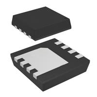


 工商网监
湘ICP备2023018690号
工商网监
湘ICP备2023018690号
