AON7410
30V N-Channel MOSFET
General Description
Features
The AON7410 uses advanced trench technology and design
to provide excellent RDS(ON) with low gate charge. This
device is suitable for use in DC - DC converters and Load
Switch applications.
VDS (V) = 30V
ID = 24A
RDS(ON) < 20mΩ
RDS(ON) < 26mΩ
RoHS and Halogen-Free Compliant
100% UIS Tested
100% Rg Tested
Top View
DFN 3x3 EP
Bottom View
(VGS = 10V)
(VGS = 10V)
(VGS = 4.5V)
D
Top View
1
8
2
7
3
6
4
5
G
Pin 1
S
Orderable Part Number
Package Type
Form
Minimum Order Quantity
AON7410
DFN 3x3 EP
Tape & Reel
5000
Absolute Maximum Ratings TA=25°C unless otherwise noted
Parameter
Drain-Source Voltage
Symbol
VDS
Maximum
30
Units
V
Gate-Source Voltage
VGS
±20
V
ID
15
TC=25°C
Continuous Drain
Current B
TC=100°C
Pulsed Drain Current C
24
IDM
Continuous Drain
A
Current
TA=70°C
A
50
TA=25°C
9.5
IDSM
7.7
Avalanche Current C
IAS, IAR
17
A
Repetitive avalanche energy L=0.1mH C
EAS, EAR
14
mJ
TC=25°C
Power Dissipation
B
TC=100°C
TA=25°C
Power Dissipation A
TA=70°C
Junction and Storage Temperature Range
Thermal Characteristics
Parameter
Maximum Junction-to-Ambient A
Maximum Junction-to-Ambient A
Maximum Junction-to-Case
Rev.12.0: August 2014
B
20
PD
8.3
PDSM
2
TJ, TSTG
-55 to 150
Symbol
t ≤ 10s
Steady-State
Steady-State
W
3.1
RθJA
RθJC
www.aosmd.com
Typ
30
60
5
°C
Max
40
75
6
Units
°C/W
°C/W
°C/W
Page 1 of 6
�Electrical Characteristics (TJ=25°C unless otherwise noted)
Parameter
Symbol
STATIC PARAMETERS
BVDSS
Drain-Source Breakdown Voltage
Conditions
Min
ID=250µA, VGS=0V
IGSS
Gate-Body leakage current
VDS=0V, VGS= ±20V
VGS(th)
Gate Threshold Voltage
VDS=VGS ID=250µA
1.4
ID(ON)
On state drain current
VGS=10V, VDS=5V
50
RDS(ON)
Static Drain-Source On-Resistance
gFS
Forward Transconductance
VSD
Diode Forward Voltage
IS
Maximum Body-Diode Continuous Current
TJ=55°C
5
±100
VGS=10V, ID=8A
Reverse Transfer Capacitance
Rg
Gate resistance
20
VGS=4.5V, ID=7A
21
26
VDS=5V, ID=8A
30
IS=1A,VGS=0V
0.75
VGS=0V, VDS=15V, f=1MHz
VGS=0V, VDS=0V, f=1MHz
Qgs
Gate Source Charge
Qgd
Gate Drain Charge
tD(on)
Turn-On DelayTime
VGS=10V, VDS=15V, ID=8A
nA
V
mΩ
S
1
V
20
A
440
550
660
pF
77
110
143
pF
33
55
77
pF
3
4
4.9
Ω
7.8
9.8
12
nC
3.6
4.6
5.5
nC
1.4
1.8
2.2
nC
1.3
2.2
3
nC
5
VGS=10V, VDS=15V, RL=2Ω,
RGEN=3Ω
ns
tr
Turn-On Rise Time
tD(off)
Turn-Off DelayTime
tf
trr
Turn-Off Fall Time
IF=8A, dI/dt=500A/µs
7
9
11
Qrr
Body Diode Reverse Recovery Charge IF=8A, dI/dt=500A/µs
12
15
18
Body Diode Reverse Recovery Time
µA
A
29
SWITCHING PARAMETERS
Qg (10V) Total Gate Charge
Qg (4.5V) Total Gate Charge
2.5
16
DYNAMIC PARAMETERS
Input Capacitance
Ciss
Crss
1.8
24
TJ=125°C
Units
V
1
Zero Gate Voltage Drain Current
Output Capacitance
Max
30
VDS=30V, VGS=0V
IDSS
Coss
Typ
3.2
ns
24
ns
6
ns
ns
nC
A: The value of RθJA is measured with the device mounted on 1in2 FR-4 board with 2oz. Copper, in a still air environment with TA =25°C. The
Power dissipation PDSM is based on RθJA t ≤ 10s value and the maximum allowed junction temperature of 150°C. The value in any given
application depends on the user's specific board design, and the maximum temperature of 150°C may be used if the PCB allows it.
B. The power dissipation PD is based on TJ(MAX)=150°C, using junction-to-case thermal resistance, and is more useful in setting the upper
dissipation limit for cases where additional heatsinking is used.
C: Repetitive rating, pulse width limited by junction temperature TJ(MAX)=150°C.
D. The RθJA is the sum of the thermal impedence from junction to case RθJC and case to ambient.
150
E. The static characteristics in Figures 1 to 6 are obtained using
很抱歉,暂时无法提供与“AON7410_106”相匹配的价格&库存,您可以联系我们找货
免费人工找货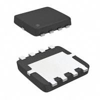


 工商网监
湘ICP备2023018690号
工商网监
湘ICP备2023018690号
