AOZ1320
Load Switch with Controlled Slew Rate
General Description
Features
The AOZ1320 is a P-channel high-side load switch with
controlled slew rate. Three slew rate options are
available. The AOZ1320-01 and AOZ1320-04 have a
slew rate of 1ms, and the AOZ1320-07 has a slew rate of
4.5ms. The AOZ1320-02 and AOZ1320-05 feature fast
Slew Rate (less than 500ns). The slew rate of
AOZ1320-03 and AOZ1320-06 is 100µs. The
AOZ1320-03, AOZ1320-04, AOZ1320-05, and
AOZ1320-07 provide an output discharge circuit to
quickly discharge the output when the switch is disabled.
1.8V to 5.5V Input Voltage Range
Input Under-Voltage Lockout
Low RDS(ON) (75mΩ Typical at 5V)
Controlled Turn-On Slew Rate
The P-channel MOSFET has typical on resistance of
75m¾. The very low RDS(ON) significantly reduces the
power path dissipation. The input voltage range of
AOZ1320 is from 1.8V to 5.5V. The control input is
compatible with both TTL and CMOS logic. Ultra low
quiescent current makes this product suitable for any
portable applications.
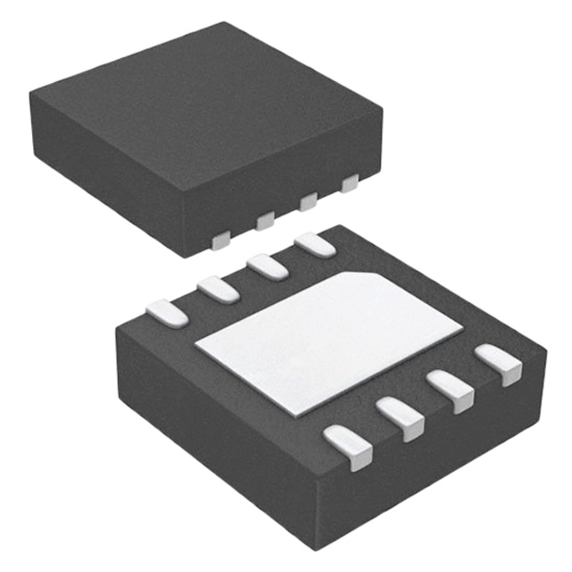
The AOZ1320 is available in a 6-pin SOT23 or
8-pin 2mm X 2mm DFN package and is rated over
the -40°C to +85°C ambient temperature range.
– 1ms (AOZ1320-01, -04)
– 0.5µs (AOZ1320-02, -05)
– 100µs (AOZ1320-03, -06)
– 4.5ms (AOZ1320-07)
Output Discharge Function (-03, -04, -05)
Low Quiescent Current (1.2µA typical)
Low Shutdown Current ( 2.5V)
6A
Maximum Pulsed Current (VIN < 2.5V)
3A
Storage Temperature (TS)
-65°C to +150°C
ESD Rating(1)
4.5kV
Rating
Operating Junction Temperature (TJ)
-40°C to +150°C
Power Dissipation
SOT23-6
2x2 DFN-8
0.65W
1.54W
Package Thermal Resistance
SOT23-6 (JA)
2x2 DFN-8 (JA)
191°C/W
81°C/W
Note:
1. Devices are inherently ESD sensitive, handling precautions are
required. Human body model is a 100pF capacitor discharging
through a 1.5k¾ resistor.
Rev. 1.8 August 2013
www.aosmd.com
Page 3 of 18
�AOZ1320
Electrical Characteristics
TA = 25°C, VIN = VEN = 5V, unless otherwise specified. Specifications in BOLD indicate an ambient temperature range of
-40°C to +85°C.
Symbol
VIN
Parameter
Conditions
Operating Voltage Range
Under-Voltage Lockout Threshold
VIN Falling
VIN Rising
IIN
Input Quiescent Current
EN = 5.0V
EN = GND
IOUT(OFF)
Switch Leakage Current
VEN < VIL(max), VOUT = 0V
RDS(ON)
Switch On-Resistance
VIN = 5.0V
VIN = 4.2V
VIN = 3.0V
VIN = 1.8V
VUVLO
VIL
Enable Input-Low Voltage
VIH
Enable Input-High Voltage
VIN = 1.8V to 2.0V
VIN = 2.0V to 4.2V
VIN = 4.2V to 5.5V
IEN
Enable Input Leakage Current
VEN = 5.5V
Min.
Typ.
Max.
Units
1.8
5
5.5
V
0.7
1.0
0.9
1.2
1.3
1.6
V
1.2
4
1
µA
1
µA
75
78
81
109
100
105
110
150
mΩ
0.8
V
V
1.8
2.0
2.4
1
µA
AOZ1320-01, -04
TD(ON)
TR
TD(OFF)
Output Turn-on delay
RL = 10Ω, See Figure 1
200
300
µs
Output Rise-time
RL = 10Ω, See Figure 1
1000
1500
µs
Output Turn-off delay
RL = 10Ω, See Figure 1
20
30
µs
Output Turn-On Delay
RL = 10Ω, See Figure 1
2
4
µs
Output Rise-Time
RL = 10Ω, See Figure 1
0.5
1
µs
Output Turn-Off Delay
RL = 10Ω, See Figure 1
20
30
µs
RL = 10Ω, See Figure 1
20
130
µs
Output Rise Time
RL = 10Ω, See Figure 1
100
150
µs
Output Turn-Off Delay
RL = 10Ω, See Figure 1
20
30
µs
Output Turn-On Delay
RL = 10Ω, See Figure 1
450
850
µs
Output Rise Time
RL = 10Ω, See Figure 1
4500
7500
µs
Output Turn-Off Delay
RL = 10Ω, See Figure 1
20
30
µs
VEN < VIL(max)
180
250
Ω
AOZ1320-02, -05
TD(ON)
TR
TD(OFF)
AOZ1320-03, -06
TD(ON)
TR
TD(OFF)
Output Turn-On Delay
AOZ1320-07
TD(ON)
TR
TD(OFF)
AOZ1320-03, -04, -05, -07
RDIS
Output Pull-Down Resistance in Shutdown
Rev. 1.8 August 2013
www.aosmd.com
Page 4 of 18
�AOZ1320
Typical Performance Characteristics
Quiescent Current vs. Temperature
Quiescent Current vs. Input Voltage
1.6
Quiescent Current (μA)
Quiescent Current (μA)
2.00
1.60
VIN = 5V
1.20
VIN = 3V
0.80
0.40
1.4
1.2
1.0
0.8
0.6
0.4
0.2
0.00
-40
0
-20
0
20
40
60
80
100
0
1
2
RDS(ON) vs. Input Voltage
6
100
1A
RDS(ON) (mΩ)
RDS(ON) (mΩ)
1.6A
500mA
120
100mA
90
VIN = 3V
80
60
1.5
VIN = 5V
70
60
80
2.0
2.5
3.0
3.5
4.0
4.5
5.0
50
-40
5.5
-20
0
Input Voltage (V)
0.30
1.80
0.25
IOFF-SW (μA)
1.60
1.40
VIH
1.20
VIL
60
80
100
0.20
0.15
0.10
0.05
0.80
0.60
1.5
40
OFF-Switch Current vs. Temperature
2.00
1.00
20
Temperature (°C)
ON/OFF Threshold vs. Input Voltage
ON/OFF Threshold (V)
5
110
140
100
4
RDS(ON) vs. Temperature
180
160
3
Input Voltage (V)
Temperature (°C)
2.0
2.5
3.0
3.5
4.0
4.5
5.0
5.5
Input Voltage (V)
Rev. 1.8 August 2013
0
-40
-20
0
20
40
60
80
100
Temperature (°C)
www.aosmd.com
Page 5 of 18
�AOZ1320
Typical Characteristics
AOZ1320-01, AOZ1320-04
Turn-On
(VIN = 3V, R = 6Ω)
CH1: On/Off (5V/div)
CH3: IIN (200mA/div)
Turn-On
(VIN = 5V, R = 10Ω)
CH2: VOUT (2V/div)
Time: 500μS/div
CH1: On/Off (5V/div)
CH3: IIN (200mA/div)
Turn-Off
(VIN = 3V, R = 6Ω)
CH1: On/Off (5V/div)
CH3: IIN (200mA/div)
Rev. 1.8 August 2013
CH2: VOUT (2V/div)
Time: 500μS/div
Turn-Off
(VIN = 5V, R = 10Ω)
CH2: VOUT (2V/div)
CH1: On/Off (5V/div)
CH3: IIN (200mA/div)
Time: 10μS/div
www.aosmd.com
CH2: VOUT (2V/div)
Time: 10μS/div
Page 6 of 18
�AOZ1320
Typical Characteristics (Continued)
AOZ1320-02, AOZ1320-05
Turn-On
(VIN = 3V, R = 6Ω)
CH1: On/Off (5V/div)
CH3: IIN (200mA/div)
Turn-On
(VIN = 5V, R = 10Ω)
CH2: VOUT (2V/div)
Time: 5μS/div
CH1: On/Off (5V/div)
CH3: IIN (200mA/div)
Turn-Off
(VIN = 3V, R = 6Ω)
CH1: On/Off (5V/div)
CH3: IIN (200mA/div)
Rev. 1.8 August 2013
CH2: VOUT (2V/div)
Time: 5μS/div
Turn-Off
(VIN = 5V, R = 10Ω)
CH2: VOUT (2V/div)
CH1: On/Off (5V/div)
CH3: IIN (200mA/div)
Time: 5μS/div
www.aosmd.com
CH2: VOUT (2V/div)
Time: 5μS/div
Page 7 of 18
�AOZ1320
Typical Characteristics (Continued)
AOZ1320-03, AOZ1320-06
Turn-On
(VIN = 3V, R = 6Ω)
CH1: On/Off (5V/div)
CH3: IIN (200mA/div)
Turn-On
(VIN = 5V, R = 10Ω)
CH2: VOUT (2V/div)
Time: 50μS/div
CH1: On/Off (5V/div)
CH3: IIN (200mA/div)
Turn-Off
(VIN = 3V, R = 6Ω)
CH1: On/Off (5V/div)
CH3: IIN (200mA/div)
Rev. 1.8 August 2013
CH2: VOUT (2V/div)
Time: 50μS/div
Turn-Off
(VIN = 5V, R = 10Ω)
CH2: VOUT (2V/div)
CH1: On/Off (5V/div)
CH3: IIN (200mA/div)
Time: 5μS/div
www.aosmd.com
CH2: VOUT (2V/div)
Time: 5μS/div
Page 8 of 18
�AOZ1320
Typical Characteristics (Continued)
AOZ1320-07
Turn-On
(VIN = 3V, R = 6Ω)
CH1: On/Off (5V/div)
CH3: IIN (200mA/div)
Turn-On
(VIN = 5V, R = 10Ω)
CH2: VOUT (2V/div)
CH1: On/Off (5V/div)
CH3: IIN (200mA/div)
Time: 4mS/div
Turn-Off
(VIN = 3V, R = 6Ω)
CH1: On/Off (5V/div)
CH3: IIN (200mA/div)
CH2: VOUT (2V/div)
Time: 4mS/div
Turn-Off
(VIN = 5V, R = 10Ω)
CH2: VOUT (2V/div)
Time: 4ms/div
CH1: On/Off (5V/div)
CH3: IIN (200mA/div)
CH2: VOUT (2V/div)
Time: 4mS/div
AOZ1320-03, AOZ1320-04, AOZ1320-05, AOZ1320-07
Turn-Off
Output Discharge
(VIN = VEN = 5V, VOUT = 5V, COUT = 4.7μF, TA = 25°C)
CH1: VEN (2V/div)
CH2: VOUT (2V/div)
Time: 400μs/div
Rev. 1.8 August 2013
www.aosmd.com
Page 9 of 18
�AOZ1320
Timing Diagram
VIH
EN
VIL
90%
90%
10%
OUT
TD(ON)
TD(OFF)
TR
Figure 1. AOZ1320 Timing Diagram
Functional Block Diagram
IN
OUT
UVLO
Comparator
Gate Driver &
Slew Rate
Control
0.9V
180Ω
AOZ1320
-3, -4, -5
+
–
EN
GND
Figure 2. Functional Block Diagram
Rev. 1.8 August 2013
www.aosmd.com
Page 10 of 18
�AOZ1320
Detailed Description
Applications Information
Slew Rate Control
Input Capacitor Selection
Use a 1µF or larger capacitor for input bypassing.
Place the capacitor close to the IN pins of AOZ1320.
The AOZ1320 is a family of P-channel high-side load
switches with controlled slew rate. The device is enabled
when the input voltage is above the Under-Voltage
Lockout (UVLO) threshold and the EN pin is high. Once
enabled, the gate driver and slew-rate control circuitry
immediately raises the source-to-gate voltage of the
P-channel MOSFET to its threshold level, and then
gradually turns on the MOSFET by linearly increases the
source-to-gate voltage. This slow turn-on action
effectively limits the input inrush current and provides
a nice ramp for the output voltage. After the MOSFET is
fully enhanced, the AOZ1320 quickly increases the
source-to-gate voltage to the full input voltage to
minimize on resistance and reduce power dissipation.
Three slew-rate options are available. AOZ1320-01
and -04 have a slew rate of 1ms, and the AOZ1320-07
has a slew rate of 4.5ms. This option significantly reduces
the inrush current when the MOSFET turns on, allowing
the use of very small input capacitor. AOZ1320-02 and
-05 have no slew rate control and the MOSFET can be
turned on within 500ns. This option is suitable for
applications that require very fast switching. AOZ1320-03
and -06 have a moderate slew rate to 100µs. The
AOZ1320-03, -04, -05, and -07 options include an
internal output discharge circuit that quickly discharges
the output to ground when the device is disabled.
Input Under-Voltage Lockout
The operating voltage range of AOZ1320 is from 1.8V
to 5.5V. An internal UVLO comparator monitors the input
voltage. The device is disabled if the input voltage falls
below the UVLO threshold (0.9V typical). The UVLO
comparator has about 300mV hysteresis.
On/Off Control
The AOZ1320 is enabled when the input voltage is above
the UVLO threshold and the EN pin is asserted high.
The device is disabled when the input voltage is below
the UVLO threshold or the EN pin is asserted low. The
EN input is compatible with both TTL and CMOS logic.
Internal Discharge Resistor
The AOZ1320 has an internal 180¾ resistor to discharge
any remaining voltage from the system to the ground
that is store in a capacitive load. This provides a safe
shutdown of the system to prevent any damages to the
devices. This function is controlled from the Enable pin.
Rev. 1.8 August 2013
Output Capacitor Selection
Use a 0.1µF or larger capacitor between OUT and GND.
The capacitance does not affect the turn-on slew rate.
However, a larger capacitor makes the initial turn-on
transient smoother.
Thermal Considerations
To ensure proper operation, the maximum junction
temperature (TJ(MAX)) of AOZ1320 should not exceed
150°C. Several factors attribute to the junction temperature
rise: load current, MOSFET on resistance (RDS(ON)), onresistance temperature coefficient (TC), junction-to-ambient
thermal resistance (JA), and ambient temperature (TA).
Use the following equation to determine the maximum
continuous load current ILOAD(MAX):
I LOAD MAX =
T J MAX – T A
--------------------------------------------------------------------------------------------------------------- JA R DS ON 1 + T C T J MAX – T A
where RDS(ON) is the maximum value of the MOSFET on
resistance at 25°C. Please note the maximum load current
should not exceed the absolute maximum current rating of
the switch. For the SOT-23 package, the absolute maximum current rating is 1.6A. For the 2x2 DFN package, the
absolute maximum current rating is 2.3A.
For example, when VIN = 5V, the maximum continuous
load current of SOT-23 package at room temperature is:
I LOAD MAX =
150C – 25C
------------------------------------------------------------------------------------------------------------------------------------------- = 2.78A
120C W 100m 1 + 0.0028 150C – 25C
Since the calculated current is greater than the absolute
maximum current rating, the maximum load current at
VIN = 5V and room temperature is 1.6A.
Exceeding the maximum continuous load current may
cause damage to the device. Figure 3 and Figure 4 show
the maximum load current as a function of the ambient
temperature for SOT23 and 2x2 DFN packages respectively. To ensure proper operation, the load current
should not exceed the limits in these two figures.
www.aosmd.com
Page 11 of 18
�2.5
2.0
VIN = 5V
1.5
VIN = 3V
1.0
0.5
0
0
20
40
60
80
100
Maximum Load Current (IO)
Maximum Load Current (IO)
AOZ1320
2.5
VIN = 5V
2.0
VIN = 3V
1.5
1.0
0.5
0
Ambient Temperature (°C)
0
20
40
60
80
100
Ambient Temperature (°C)
Figure 3. Maximum Load Current
Thermal Derating for SOT23 Package
Figure 4. Maximum Load Current
Thermal Derating for 2x2 DFN Package
Layout Guidelines
Good PCB is important for improving the thermal performance of AOZ1320. Place the input and output bypass
capacitors close to the IN and OUT pins. The input and
output PCB traces should be as wide as possible for the
given PCB space. Use a ground plane to enhance the
power dissipation capability of the device. The AOZ1320
evaluation board can be used as a layout example. The
PCB layout of AOZ1320 evaluation board is shown in
Figure 5 and 6.
Figure 5. AOZ1320 (SOT23-6) PCB Layout
Rev. 1.8 August 2013
www.aosmd.com
Page 12 of 18
�AOZ1320
Figure 6. AOZ1320 (DFN2x2) PCB Layout
Rev. 1.8 August 2013
www.aosmd.com
Page 13 of 18
�AOZ1320
Package Dimensions, SOT23-6 LP
Gauge Plane
D
Seating Plane
L2
e1
c
6
L
E E1
1
θ
e
b
A2
A
aaa
A1
Dimensions in millimeters
RECOMMENDED LAND PATTERN
2.40
0.80
0.95
0.63
UNIT: mm
Dimensions in inches
Symbols
A
A1
A2
Min.
—
0.00
0.70
Nom.
—
—
0.88
Max.
1.00
0.10
0.95
Symbols
A
A1
A2
Min.
—
0.00
0.028
Nom.
—
—
0.035
Max.
0.039
0.004
0.037
b
c
D
E
E1
0.35
0.10
2.80
2.60
1.50
0.40
0.13
2.90
2.80
1.60
0.50
0.20
3.00
3.00
1.70
b
c
D
E
E1
0.014
0.004
0.110
0.102
0.059
0.016
0.005
0.114
0.110
0.063
0.020
0.008
0.118
0.118
0.067
e
e1
L
L2
aaa
0.95 BSC
1.90 BSC
0.30
0.40
0.60
0.25 BSC
0.10
e
e1
L
L2
aaa
0.037 BSC
0.075 BSC
0.012 0.016 0.024
0.010 BSC
0.004
θ
0°
—
8°
θ
0°
—
8°
Notes:
1. Package body sizes exclude mold flash and gate burrs. Mold flash at the non-lead sides should be less than 5 mils each.
2. Dimension “L” is measured in gauge plane.
3. Tolerance ±0.100mm (4 mil) unless otherwise specified.
4. Refer to JEDEC MO-193C AB.
6. Controlling dimension is millimeter. Converted inch dimensions are not necessarily exact.
Rev. 1.8 August 2013
www.aosmd.com
Page 14 of 18
�AOZ1320
Tape and Reel Dimensions, SOT23-6
Tape
P2
P1
D1
D0
E1
K0
E2
E
B0
A0
P0
Feeding Direction
Unit: mm
Package
A0
B0
K0
D0
D1
E
E1
E2
P0
P1
P2
T
SOT23-5/6L
LP
3.15
±0.10
3.20
±0.10
1.40
±0.10
1.50
±0.05
1.00
+0.10 / -0
8.00
±0.30
1.75
±0.10
3.50
±0.05
4.00
±0.10
4.00
±0.10
2.00
±0.05
0.23
±0.03
Reel
W1
S
K
R
M
N
J
H
Unit: mm
Tape Size
Reel Size
M
N
8mm
ø177.8
ø177.8
Max.
55.0
Min.
W1
H
8.4
13.0
+1.50 / -0.0 +0.5 / -0.2
S
K
R
J
1.5
Min
10.1
Min.
12.7
4.0
±0.1
Leader/Trailer and Orientation
Trailer Tape
300mm min.
Rev. 1.8 August 2013
Components Tape
Orientation in Pocket
www.aosmd.com
Leader Tape
500mm min.
Page 15 of 18
�AOZ1320
Package Dimensions, DFN 2x2 8L
b
D
E
R
E1
E
L
D1
TOP VIEW
A
c
BOTTOM VIEW
A1
Seating
Plane
SIDE VIEW
Dimensions in millimeters
RECOMMENDED LAND PATTERN
0.50
0.25
0.90
0.30
1.50
UNIT: mm
1.70
Symbols
A
A1
b
c
D
D1
E
Min.
0.70
0.00
0.18
0.15
Nom.
0.75
0.02
0.25
0.20
2.00 BSC
1.35
1.50
2.00 BSC
E1
e
L
R
aaa
bbb
0.75
Dimensions in inches
Symbols
A
A1
b
c
D
D1
E
Min.
0.028
0.000
0.007
0.006
0.90
1.00
0.50 BSC
0.20
0.30
0.40
0.20
0.15
0.10
E1
e
L
R
aaa
bbb
0.030
0.10
0.08
ccc
ddd
ccc
ddd
Max.
0.80
0.05
0.30
0.25
1.60
Nom. Max.
0.030 0.031
0.001 0.002
0.010 0.012
0.008 0.010
0.079 BSC
0.053 0.059 0.063
0.079 BSC
0.035 0.039
0.020 BSC
0.008 0.012 0.016
0.008
0.006
0.004
0.004
0.003
Notes:
1. Dimensions and tolerances conform to ASME Y14.5M-1994.
2. Controlling dimension is millimeter, converted inch dimensions are not necessarily exact.
3. Dimension b applied to metallized terminal and is measured between 0.10mm and 0.30mm from the terminal tip. If the terminal
has the optional radius on the other end of the terminal, dimension b should not be measured in that radius area.
4. Coplanarity ddd applies to the terminals and all other bottom surface metallization.
Rev. 1.8 August 2013
www.aosmd.com
Page 16 of 18
�AOZ1320
Tape and Reel Dimensions, DFN 2 x 2
Carrier Tape
P2
P1
D0
D1
E1
K0
E2
B0
T
E
A0
P0
Feeding Direction
UNIT: mm
Package
DFN 2x2
A0
2.25
±0.05
B0
2.25
±0.05
K0
D0
D1
E
E1
1.00
1.50
1.00
8.00
1.75
±0.05 +0.10/-0 +0.25/-0 +0.30/-0.10 ±0.10
Reel
E2
3.50
±0.05
P0
4.00
±0.10
P1
4.00
±0.10
P2
2.00
±0.10
T
0.254
±0.02
W1
S
R
K
M
N
H
UNIT: mm
Tape Size Reel Size
M
8mm
ø180
ø180.00
±0.50
N
60.0
±0.50
W1
8.4
+1.5/-0.0
H
13.0
±0.20
S
1.5
Min.
K
13.5
Min.
R
3.0
±0.50
Leader / Trailer
& Orientation
Trailer Tape
300mm Min.
Rev. 1.8 August 2013
Components Tape
Orientation in Pocket
www.aosmd.com
Leader Tape
500mm Min.
Page 17 of 18
�AOZ1320
Package Marking
AOZ1320CI
AA 0W
LT
(SOT23-6)
Assembly Lot Code
Week & Year Code
Part Number Code
Option/Assembly Code
AOZ1320DI
(DFN2x2-8)
AB OA
Part Number Code
YW LT
Week & Year Code
Assembly Location Code
Option Code
Assembly Lot Code
LEGAL DISCLAIMER
Alpha and Omega Semiconductor makes no representations or warranties with respect to the accuracy or
completeness of the information provided herein and takes no liabilities for the consequences of use of such
information or any product described herein. Alpha and Omega Semiconductor reserves the right to make changes
to such information at any time without further notice. This document does not constitute the grant of any intellectual
property rights or representation of non-infringement of any third party’s intellectual property rights.
LIFE SUPPORT POLICY
ALPHA AND OMEGA SEMICONDUCTOR PRODUCTS ARE NOT AUTHORIZED FOR USE AS CRITICAL
COMPONENTS IN LIFE SUPPORT DEVICES OR SYSTEMS.
As used herein:
1. Life support devices or systems are devices or
systems which, (a) are intended for surgical implant into
the body or (b) support or sustain life, and (c) whose
failure to perform when properly used in accordance
with instructions for use provided in the labeling, can be
reasonably expected to result in a significant injury of
the user.
Rev. 1.8 August 2013
2. A critical component in any component of a life
support, device, or system whose failure to perform can
be reasonably expected to cause the failure of the life
support device or system, or to affect its safety or
effectiveness.
www.aosmd.com
Page 18 of 18
���


 工商网监
湘ICP备2023018690号
工商网监
湘ICP备2023018690号
