General Description
Features
The AOZ6134 is a high performance single-pole
double-throw (SPDT), low power, TTL-compatible bus
switch.
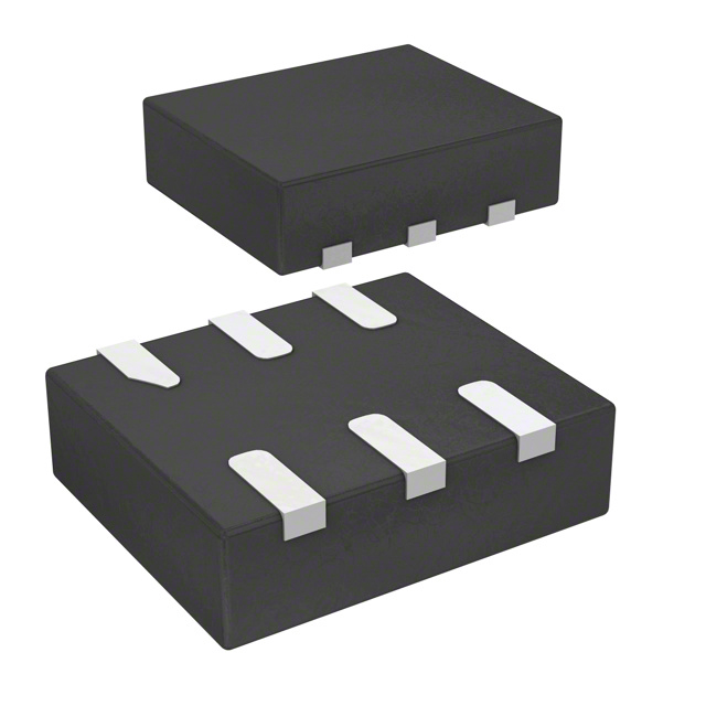
DFN 1.2 mm x 1.0 mm x 0.55 mm 6-Lead Package
The AOZ6134 will accept analog and digital signals.
Signals with voltages up to VCC (1.65 V to 5.5 V) can be
transmitted in either direction.
Break-before-make switching
1.65 V to 5.5 V VCC operation
1
connection between ports
When the Select pin is LOW, B0 is connected to the
output A pin. When the Select pin is HIGH, B1 is
connected to the output A pin. The path that is open will
have a high-impedance state with respect to the output.
Break-before-make is guaranteed.
Typical Application
)\XIVREP
1-'
1-'�4VI�%QT
'3()'
-RXIVREP
1-'
Rev. 0.5 February 2012
www.aosmd.com
Page 1 of 9
�AOZ6134
Ordering Information
Part Number
Ambient Temperature Range
Package
Environmental
AOZ6134DI
-40 °C to +85 °C
DFN 1.2 mm x 1.0 mm, 6L
RoHS Compliant
Green Product
AOS Green Products use reduced levels of Halogens, and are also RoHS compliant.
Please visit www.aosmd.com/web/quality/rohs_compliant.jsp for additional information.
Pin Configuration
&�
�
�
7
+2(
�
�
:GG
&�
�
�
%
(*2��
�8ST�8LVY�:MI[
Truth Table
Logic S Input
Function
0
B0 Connected to A
1
B1 Connected to A
Rev. 0.5 February 2012
www.aosmd.com
Page 2 of 9
�AOZ6134
Absolute Maximum Ratings
Exceeding the Absolute Maximum ratings may damage the device.
Symbol
Parameter
VCC
Supply Voltage
Switch
VS
Rating
-0.5 V to +6 V
Voltage(1)
-0.5 V to VCC
Voltage(1)
VIN
Input
IIK
Minimum Input Diode Current(2)
-50 mA
ISW
Switch Current
200 mA
Peak Switch Current (Pulsed at 1 ms, < 10% Duty Cycle)
400 mA
ISWPEAK
-0.5 V to VCC
Storage Temperature Range
TSTG
-65 °C to +150 °C
Maximum Junction Temperature
TJ
DFN-6 Power Dissipation at 85
PD
ESD
+150 °C
°C(3)
560 mW
Human Body Model (JESD22A-114E)
8000 V
Recommend Operating Ratings
The device is not guaranteed to operate beyond the Maximum Operating Ratings.
Symbol
VCC
Parameter
Supply Voltage
1.65 V to +5.5 V
Voltage (4)
VIN
Control Input
VSW
Switch Input Voltage
TA
Rating
0 V to VCC
0 V to VCC
Operating Temperature
-40 °C to +85 °C
Notes:
1. Signals on A, or B or S exceeding V+ will be clamped by internal diodes. Limit forward diode current to maximum current ratings.
2. Negative current should not exceed minimum negative value.
3. All leads welded or soldered to PC Board.
4. Unused inputs must be held HIGH or LOW. They may not float.
Rev. 0.5 February 2012
www.aosmd.com
Page 3 of 9
�AOZ6134
Electrical Characteristics
Unless otherwise indicated, specifications indicate a temperature range of -40 °C to +85 °C. All typical values are at 25 °C unless
otherwise specified.
Symbol
Parameter
Test Conditions
VCC (V)
Min.
1.65 to 2.7
1.0
2.7 to 3.6
1.5
4.5 to 5.5
2.0
Typ.
Max.
Units
DC CHARACTERISTICS
VIH
VIL
Input Voltage High
Input Voltage Low
V
1.65 to 2.7
0.4
2.7 to 3.6
0.6
4.5 to 5.5
RON
RFLAT
RON
IIN
On Resistance
On Resistance
Flatness
On Resistance
Matching Between
Channels
0.8
IOUT =100 mA,
B0 or B1 = 0 V, 1.5 V, 2.5 V, 3.5 V,
3.75 V, or 4.5 V
4.5
0.6
1.2
IOUT = 100 mA,
B0 or B1 = 0 V, 1.5 V, 2 V, or 2.7 V
2.7
1.0
1.5
IOUT =100mA,
B0 or B1 = 0 V, 1.25 V, 1.5 V, or 1.8 V
1.8
3.0
6.0
IOUT =100 mA,
B0 or B1 = 0 V to VCC
4.5
0.2
2.7
0.4
1.8
2.5
4.5
0.03
IOUT =100 mA, B0 or B1 = 1.5 V
V
0.15
IOUT =100 mA, B0 or B1 = 3.5 V
Input Leakage
Current
VIN = 0 V or VCC
1.95 to 5.5
±1.0
µA
IB(off)
Off Stage Switch
Leakage
A = 1 V, 4.5 V,
B0 or B1 = 4.5 V, 1 V
1.95 to 5.5
±30
nA
IA(on)
On State Switch
Leakage
A = 1 V, 4.5 V,
B0 or B1 = 4.5 V, 1 V or floating
1.95 to 5.5
±40
nA
POWER SUPPLY
VCC
Power Supply Range
ICCQ
Quiescent Supply
Current
VIN = 0 V or VCC, IOUT = 0 V
5.5
ICCT
Increase in ICC
per Input
VIN = 1.8 V
5.5
Rev. 0.5 February 2012
1.65 to 5.5
VIN = 2.6 V
www.aosmd.com
1.65
5.5
V
0.5
µA
30
40
µA
18
25
Page 4 of 9
�AOZ6134
Electrical Characteristics (Continued)
Unless otherwise indicated, specifications indicate a temperature range of -40 °C to +85 °C. All typical values are at 25 °C unless
otherwise specified.
Symbol
Parameter
VCC (V)
Test Conditions
Min.
Typ.
Max.
Units
2.7 to 3.6
70
65
ns
4.5 to 5.5
55
55
2.7 to 3.6
50
45
4.5 to 5.5
45
45
AC CHARACTERISTICS
tON
tOFF
tBBM
Q
Turn-On Time
B0 or B1 = 1.5 V, RL = 50
CL = 35 pF
Turn-Off Time
B0 or B1 = 1.5 V, RL = 50
CL = 35 pF
,
,
Break-Before-Make
Time
Charge Injection
(2)
1.65 to 1.95
CL = 1.0 nF, VGE = 0 V, RGEN = 0
20
2.3 to 2.7
15
3.0 to 3.65
10
4.5 to 5.5
10
4.5 to 5.5
90
2.7 to 3.6
50
ns
ns
pC
ANALOG SWITCH CHARACTERISTICS(2)
OIRR
Off Isolation
RL = 50
, f = 1 MHz
2.7 to 5.5
-60
dB
XTALK
Crosstalk
RL = 50
, f = 1 MHz
2.7 to 5.5
-60
dB
BW
-3 dB Bandwidth
RL = 50
2.7 to 5.5
180
MHz
THD
Total Harmonic
Distortion
VIN = 2 Vpk-pk, f = 20 Hz to 20 kHz
2.7 to 5.5
0.002
%
CAPACITANCE(3)
CIN
Control Pin
Capacitance
f = 1 MHz, Vbias = 1.5 V
4.5
3.0
pF
COFF
B Port Off
Capacitance
f = 1 MHz, Vbias = 1.5 V
4.5
7.0
pF
CON
A Port Capacitance
When Switch Enable
f = 1 MHz, Vbias = 1.5 V
4.5
40.0
pF
Notes:
1. Typical values are for design aid only, not guaranteed nor subject to production testing.
2. TA = +25 °C, parameters are characterized but not tested in production and guaranteed by design.
3. TA = +25 °C, f = 1 MHz, capacitance is characterized but not tested in production.
Rev. 0.5 February 2012
www.aosmd.com
Page 5 of 9
�AOZ6134
AC Loading and Waveforms
:GG
'SRXVSP�
-RTYX
:398
:&
60
��
X
:GG
6 ! X * ! ���R7
��
�:
X 3**
'0
��T*
:398
7[MXGL�
�
3YXTYX
+2(
����\�:398
����\�:398
X 32
0SKMG�MRTYX�[EZIJSVQ�EVI�MRZIVXIH�JSV�W[MXGLIW�[MXL�STTSWMXI�
PSKMG�WIRWI
'0�-RGPYHIW�*M\XYVI�ERH�7XVE]�'ETEGMXERGI
*MKYVI����8YVR�3R�8YVR�3JJ�8MQMRK
:GG
:GG
&2
&2
%
%
�
�
�
7
7
�
�
+2(
*MKYVI����3JJ�7XEXI�0IEOEKI�'YVVIRX
+2(
*MKYVI����3R�7XEXI�0IEOEKI�'YVVIRX
:GG
&�
:&
%
&�
:398
60
��
7
'SRXVSP�
-RTYX
'0
��T*
:GG
��
�:
X
6 ! X * ! ���R7
:398
+2(
����\�:398
X(
'0�-RGPYHIW�*M\XYVI�ERH�7XVE]�'ETEGMXERGI
*MKYVI����&VIEO�&IJSVI�1EOI�8MQMRK
2IX[SVO
%REP]^IV
:GG
&�
:-2
:398
��
%
2IX[SVO
%REP]^IV
:GG
&�
��
7SYVGI
7MKREP
&�
%
:-2
:398
��
7SYVGI
7MKREP
��
7
:GG�SV��:
�
7
��
:GG�SV��:
�
��
+2(
+2(
*MKYVI����'VSWWXEPO
*MKYVI����3JJ�-WSPEXMSR
Rev. 0.5 February 2012
www.aosmd.com
Page 6 of 9
�AOZ6134
AC Loading and Waveforms (Continued)
:GG
&2
%
�
7
�
+2(
*MKYVI����3R�7XEXI�6IWMWXERGI
:GG
6 +)2
%
: +)2
:398
:398
& � SV & �
-RTYX�
'SRXVSP
'0
-2
:398
3**
7
3**
32
+2(
32
3**
-2
3**
5�!�� :398
�'0
*MKYVI����'LEVKI�-RNIGXMSR
:GG
��R*
:GG
2IX[SVO�%REP]^IV
��
&2
%
%
7
'ETEGMXERGI�
1IXIV
J�!��1,^
& � SV & �
7SYVGI
7MKREP
�:
SV
:GG
7
�
��
+2(
+2(
*MKYVI����32�3JJ�'ETEGMXERGI�1IEWYVIQIRX
*MKYVI�����&ERH[MHXL
:GG
%YHMS�%REP]^IV
���
%
&2
'0
7SYVGI
7MKREP
7
�
���
+2(
'0�-RGPYHIW�*M\XYVI�ERH�7XVE]�'ETEGMXERGI
*MKYVI�����,EVQSRMG�(MWXSVXMSR
Rev. 0.5 February 2012
www.aosmd.com
Page 7 of 9
�AOZ6134
Package Dimensions, DFN 1.2 mm x 1.0 mm, 6L
(
%
)
G
%�
4MR���(SX�
F]�1EVOMRK
7-()�:-);
834�:-);
F���\
I
0���\
�
0�
&38831�:-);
6)'311)2()(�0%2(�4%88)62
(MQIRWMSRW�MR�QMPPMQIXIVW
�������\
�������\
7]QFSPW
%
%�
F
G
(
)
I
0
0�
����
����
����
����
1MR�
����
����
����
2SQ�
����
h
����
������6IJ�
1E\�
����
����
����
����
����
����
����
����
�����
�����&7'
����
����
����� �����
(MQIRWMSRW�MR�MRGLIW
7]QFSPW
%
%�
F
G
(
)
I
0
0�
2SQ� 1E\�
����� �����
�����
h
����� �����
������6IJ�
����� ����� �����
����� ����� �����
������&7'
����� ����� �����
����� ����� �����
1MR�
�����
�����
�����
����
92-8��QQ
2SXI�
�� 'SRXVSPPMRK�HMQIRWMSR�MW�QMPPMQIXIV��GSRZIVXIH�MRGL�HMQIRWMSRW�EVI�RSX�RIGIWWEVMP]�I\EGX�
Rev. 0.5 February 2012
www.aosmd.com
Page 8 of 9
�AOZ6134
Part Marking
%3>����(�����\�����(*2��
4EVX�2YQFIV�
(EXI�'SHI
This datasheet contains preliminary data; supplementary data may be published at a later date.
Alpha & Omega Semiconductor reserves the right to make changes at any time without notice.
LIFE SUPPORT POLICY
ALPHA & OMEGA SEMICONDUCTOR PRODUCTS ARE NOT AUTHORIZED FOR USE AS CRITICAL
COMPONENTS IN LIFE SUPPORT DEVICES OR SYSTEMS.
As used herein:
1. Life support devices or systems are devices or
systems which, (a) are intended for surgical implant into
the body or (b) support or sustain life, and (c) whose
failure to perform when properly used in accordance
with instructions for use provided in the labeling, can be
reasonably expected to result in a significant injury of
the user.
Rev. 0.5 February 2012
2. A critical component in any component of a life
support, device, or system whose failure to perform can
be reasonably expected to cause the failure of the life
support device or system, or to affect its safety or
effectiveness.
www.aosmd.com
Page 9 of 9
�


 工商网监
湘ICP备2023018690号
工商网监
湘ICP备2023018690号
