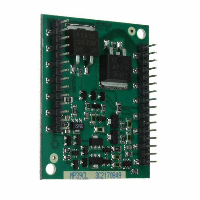
MP39 • MP39A
Power Operational Amplifier
RoHS
COMPLIANT
FEATURES
•
•
•
•
•
High Internal Dissipation — 125 Watts
High Voltage, High Current — 100V, 10A
Slew Rate — 10V/µs
4 Wire Current Limit Sensing
Optional Boost Voltage Inputs
APPLICATIONS
•
•
•
•
Linear And Rotary Motor Drives
Yoke/Magnetic Field Excitation
Programmable Power Supplies to ±45V
Industrial Audio
DESCRIPTION
The MP39 is a cost-effective high voltage MOSFET power operational amplifier constructed with surface
mount components on a thermally conductive but electrically isolated substrate.
While the cost is low the MP39 offers many of the same features and performance specifications found in
much more expensive hybrid power amplifiers.
The metal substrate allows the MP39 to dissipate power up to 125 watts and its power supply voltages
can range up to +/- 50 Volts (100V total). Optional boost voltage inputs allow the small signal portion of the
amplifier to operate at higher supply voltages than the high current output stage. The amplifier is then biased
to achieve close linear swings to the supply rails at high current for extra efficient operation. External compensation tailors performance to the user needs. A four-wire sense technique allows current limiting without
the need to consider internal or external mili-ohm parasitic resistance in the output line. An Iq pin is available
which can be used to shut off the quiescent current in the output stage. The output stage then operates class
C and lowers quiescent power dissipation. This is useful in applications where output crossover distortion is
not important.
www.apexanalog.com
© Apex Microtechnology Inc.
All rights reserved
Mar 2016
MP39U Rev K
�MP39 • MP39A
Figure 1: Equivalent Schematic
12 +Vs
+Vb 1
R1
R2
Q1A
Q1B
C1
GND 2
13 +Vs
C2
R3
14 +Vs
Q5
Q3
D1
R4
Q4
Cc2 4
Q9
Cc1 6
Q7
Q6
-IN 30
+IN 29
24 +Ilim
R5
23 -Ilim
Q10B
Q10A
R6
R8
15 OUT
Q8
16 OUT
R9
R7
17 OUT
R10
Q11
Iq 25
R11
Q12
GND 28
Q13
Q14
R12
R13
18 -Vs
C3
19 -Vs
20 -Vs
-Vb 26
TYPICAL CONNECTION
Figure 2: Typical Connection
RF
+VS +VB
10μF
1μF
1μF
RI
+VS
-IN
+IN
-VS
+VB
-CL
MP39
-VB
CC
IQ
CC
+CL
OUT
RC
RCL
VOUT
RL
RC
NC
10μF
2
1μF
-VS -VB
1μF
MP39U Rev K
�MP39 • MP39A
PINOUT AND DESCRIPTION TABLE
Figure 3: External Connections
Pin Number
Name
Description
1
+VB
The positive boost supply rail. Short to +Vs if unused. See applicable section.
2, 28
GND
Ground. Pins 2 and 28 are not connected on the unit. Connect both pins to system
signal ground.
4
CC
Compensation capacitor connection. Select value based on Phase Compensation.
See applicable section.
6
RC
Compensation resistor connection. Select value based on Phase Compensation.
See applicable section.
12, 13, 14
+Vs
The positive supply rail.
15, 16, 17
OUT
The output. Connect these pins to load and to the feedback resistor.
18, 19, 20
-Vs
The negative supply rail.
23
-CL
Connect to the load side of the current limit resistor. Current limit will activate as
the voltage across RCL increases.
24
+CL
Connect to the OUT side of the current limit resistor. Current limit will activate as
the voltage across RCL increases.
25
IQ
Quiescent current reduction pin. Connect to pin 6 to disable the AB bias. See applicable
section.
26
-VB
The negative boost supply rail. Short to -Vs if unused. See applicable section.
29
+IN
The non-inverting input.
30
-IN
The inverting input.
All Others
NC
No connection.
MP39U Rev K
3
�MP39 • MP39A
SPECIFICATIONS
Unless otherwise noted: TC = 25°C, RC = 100 Ω, CC = 470pF. DC input specifications are ± value given. Power
supply voltage is typical rating. ±VB = ±VS.
ABSOLUTE MAXIMUM RATINGS
Parameter
Symbol
Supply Voltage, +Vs To -Vs
Min
+Vs to -Vs
Boost Voltage
Max
Units
100
V
±VS ±20
V
Output Current, within SOA
IO
25
A
Power Dissipation, internal
PD
125
W
Input Voltage, differential
VIN (Diff)
-20
+20
V
Vcm
-VB
+VB
V
200
°C
175
°C
-40
+105
°C
-40
+85
°C
Input Voltage, common mode
Temperature, pin solder, -10s
Temperature, junction 1
TJ
Temperature, storage
TC
Operating Temperature Range, case
1. Long term operation at the maximum junction temperature will result in reduced product life. Derate internal power dissipation to achieve high MTTF. For guidance, refer to the heatsink data sheet.
CAUTION
The MP39 is constructed from MOSFET transistors. ESD handling procedures must be
observed.
INPUT
Parameter
Test
Conditions
MP39
Min
Offset Voltage, initial
Offset Voltage vs. temperature
Full temp range
Offset Voltage vs. supply
Offset Voltage vs. power
Full temp range
Bias Current, initial
Typ
Max
5
10
Min
Typ
Max
Units
*
3
mV
50
*
µV/°C
15
*
µV/V
30
*
µV/W
10
Bias Current vs. Supply
MP39A
200
*
0.01
100
*
*
pA/V
Offset Current, initial
10
Input Impedance, DC
1010
*
Ω
20
*
pF
Input Capacitance
50
pA
30
pA
Common Mode Voltage Range
Full temp range ±VB∓15 ±VB∓12
*
*
V
Common Mode Rejection, DC
Full temp range,
VCM= ±20V
*
*
dB
Input Noise
100 kHz BW, RS =
1 kΩ
*
µV RMS
4
86
98
10
MP39U Rev K
�MP39 • MP39A
GAIN
Parameter
Test
Conditions
MP39
Min
Typ
94
113
MP39A
Max
Min
Typ
Max
Units
*
*
dB
Open Loop, @ 15Hz
Full temp range,
CC = 100pF
Gain Bandwidth Product
IO = 10A
2
*
MHz
Power Bandwidth
RL=10 Ω, VO =
90VP-P CC =
100pF
40
*
kHz
Phase Margin
Full temp range
60
*
°
Test
Conditions
MP39
MP39A
OUTPUT
Parameter
Min
Typ
Max
Min
Typ
Max
Units
Voltage Swing
I O=10A
±VS∓8.8 ±VS∓6.0
*
*
V
Voltage Swing
±VB = ±VS ±10V,
±VS∓6.8 ±VS∓1.1
I O=10A
*
*
V
Settling Time to 0.1%
A V=+1,10V step,
R L =4 Ω
*
µs
Slew Rate
A V= –10, CC=
100pF
10
*
V/µs
Capacitive Load
Full temp range,
A V=+1
10
*
nF
2.5
Resistance
4
Current, Continuous
*
10
Ω
11
A
POWER SUPPLY
Parameter
Voltage
MP39
MP39A
Test
Conditions
Min
Typ
Max
Min
Typ
Max
Units
Full temp range
±15
±40
±50
*
*
*
V
Current, quiescent,
boost supply
22
*
mA
Current, quiescent, total
26
*
mA
MP39U Rev K
5
�MP39 • MP39A
THERMAL
Parameter
Test
Conditions
Resistance, AC, junction to case 1
Full temp range,
F>60 Hz
Resistance, DC, junction to case
Full temp range,
FK��
30
20
10
1
1k
10k
100k
1M
Frequency (Hz)
0
100
200
300
400
500
�džƚ��ŽŵƉĞŶƐĂƟŽŶ��ĂƉĂĐŝƚŽƌ�;Ɖ&Ϳ
Figure 10: Output Voltage Swing
9
Output Voltage Drop
From Supply, VS - VO (V)
8
7
+V B =
6
+V S
-V S =
-V B
5
0V
4
VS
3
-V B
=-
-1
V
= +V S
+V B
2
+ 10
1
0
0
2
4
6
8
10
Output Current, IO (A)
8
MP39U Rev K
�MP39 • MP39A
SAFE OPERATING AREA (SOA)
100
KƵƚƉƵƚ��ƵƌƌĞŶƚ͕�/O (A)
10ms
1ms
10
125°C
1
85°C
25°C
0.1
1
10
100
^ƵƉƉůLJ�ƚŽ�KƵƚƉƵƚ��ŝīĞƌĞŶƟĂů͕�VS-VO (V)
MP39U Rev K
9
�MP39 • MP39A
GENERAL
Please read Application Note 1 “General Operating Considerations” which covers stability, supplies,
heat sinking, mounting, current limit, SOA interpretation, and specification interpretation. Visit
www.apexanalog.com for Apex Microtechnology’s complete Application Notes library, Technical Seminar
Workbook, and Evaluation Kits.
CURRENT LIMIT
The two current limit sense lines are to be connected directly across the current limit sense resistor. For
the current limit to work correctly pin 24 must be connected to the amplifier output side and pin 23 connected to the load side of the current limit resistor, RLIM, as shown in Figure 11. This connection will bypass
any parasitic resistances, Rp, formed by sockets and solder joints as well as internal amplifier losses. The current limiting resistor may not be placed anywhere in the output circuit except where shown in Figure 11.
The value of the current limit resistor can be calculated as follows:
0.7V
R LIM = -----------------------I LIMIT A
Figure 11: Current Limit
TYPICAL APPLICATION
Ref: Application Note 25
The high power bandwidth and high voltage output of the MP39 allows driving ultra-sonic transducers via
a resonant circuit including the transducer and a matching transformer. The load circuit appears resistive to
the MP39.
10
MP39U Rev K
�MP39 • MP39A
Figure 12: Typical Application
BOOST OPERATION
With the VB feature the small signal stages of the amplifier are operated at higher supply voltages than
the amplifier's high current output stage. +VS (pins 12-14) and –VS (pins 18-20) are connected to the high current output stage. An additional 10V on the VB pins is sufficient to allow the small signal stages to drive the
output transistors into saturation and improve the output voltage swing for extra efficient operation when
required. When close swing to the supply rails is not required the +VB and +VS pins must be strapped together
as well as the –VB and –VS pins. The boost voltage pins must not be at a voltage lower than the VS pins.
BYPASSING
Proper bypassing of the power supply pins is crucial for proper operation. Bypass the ±Vs pins with a aluminum electrolytic capacitor with a value of at least 10µF per amp of expected output current. In addition a
0.47µF to 1µF ceramic capacitor should be placed in parallel with each aluminum electrolytic capacitor. Both
of these capacitors have to be placed as close to the power supply pins as physically possible. If not connected to the Vs pins (See BOOST OPERATION) the VB pins should also be bypassed with a .47µF to 1µF
ceramic capacitor.
USING THE IQ PIN FUNCTION
Pin 25 (Iq) can be tied to pin 6 (Cc) to eliminate the class AB biasing current from the output stage. Typically this would remove 1-4 mA of quiescent current. The resulting decrease in quiescent power dissipation
may be important in some applications. Note that implementing this option will raise the output impedance
of the amplifier and increase crossover distortion as well.
MP39U Rev K
11
�MP39 • MP39A
COMPENSATION
The external compensation components CC and RC are connected to pins 4 and 6. Unity gain stability can
be achieved at any compensation capacitance greater than 470 pF with at least 60 degrees of phase margin.
At higher gains more phase shift can be tolerated in most designs and the compensation capacitance can
accordingly be reduced, resulting in higher bandwidth and slew rate.
Gain
CC
RC
1
470pF
100Ω
≥3
220pF
Short
≥10
100pF
Short
APPLICATION REFERENCES
For additional technical information please refer to the following application notes.
AN01 General Operating Considerations
AN11 Thermal Techniques
AN38 Loop Stability with Reactive Loads
12
MP39U Rev K
�MP39 • MP39A
PACKAGE OPTIONS
Part Number
Apex Package Style
Description
MP39
CL
30-pin Open Frame
MP39A
CL
30-pin Open Frame
PACKAGE STYLE CL
MP39U Rev K
13
�MP39 • MP39A
NEED TECHNICAL HELP? CONTACT APEX SUPPORT!
For all Apex Microtechnology product questions and inquiries, call toll free 800-546-2739 in North America. For
inquiries via email, please contact apex.support@apexanalog.com. International customers can also request
support by contacting their local Apex Microtechnology Sales Representative. To find the one nearest to you,
go to www.apexanalog.com
IMPORTANT NOTICE
Apex Microtechnology, Inc. has made every effort to insure the accuracy of the content contained in this document. However, the information is
subject to change without notice and is provided "AS IS" without warranty of any kind (expressed or implied). Apex Microtechnology reserves the right
to make changes without further notice to any specifications or products mentioned herein to improve reliability. This document is the property of
Apex Microtechnology and by furnishing this information, Apex Microtechnology grants no license, expressed or implied under any patents, mask
work rights, copyrights, trademarks, trade secrets or other intellectual property rights. Apex Microtechnology owns the copyrights associated with the
information contained herein and gives consent for copies to be made of the information only for use within your organization with respect to Apex
Microtechnology integrated circuits or other products of Apex Microtechnology. This consent does not extend to other copying such as copying for
general distribution, advertising or promotional purposes, or for creating any work for resale.
APEX MICROTECHNOLOGY PRODUCTS ARE NOT DESIGNED, AUTHORIZED OR WARRANTED TO BE SUITABLE FOR USE IN PRODUCTS USED FOR LIFE
SUPPORT, AUTOMOTIVE SAFETY, SECURITY DEVICES, OR OTHER CRITICAL APPLICATIONS. PRODUCTS IN SUCH APPLICATIONS ARE UNDERSTOOD TO BE
FULLY AT THE CUSTOMER OR THE CUSTOMER’S RISK.
Apex Microtechnology, Apex and Apex Precision Power are trademarks of Apex Microtechnology, Inc. All other corporate names noted herein may be
trademarks of their respective holders.
14
MP39U Rev K
�


 工商网监
湘ICP备2023018690号
工商网监
湘ICP备2023018690号
