PA02 • PA02A
Power Operational Amplifiers
RoHS
COMPLIANT
FEATURES
•
•
•
•
•
•
•
•
High Power Bandwidth — 350 kHz
High Slew Rate — 20V/µs
Fast Settling Time — 600ns
Low Crossover Distortion — Class A/B
Low Internal Losses — 1.2V at 2A
High Output Current — ±5A Peak
Low Input Bias Current — FET Input
Isolated Case — 300 VDC
APPLICATIONS
•
•
•
•
Motor, Valve and Actuator Control
Magnetic Deflection Circuits up to 5A
Power Transducers up to 350 kHz
Audio Amplifiers up to 30W RMS
DESCRIPTION
The PA02 and PA02A are wide-band, high output current operational amplifiers designed to drive resistive, inductive and capacitive loads. Their complementary “collector output” stage can swing close to the supply rails and is protected against inductive kickback. For optimum linearity, the output stage is biased for class
A/B operation. The safe operating area (SOA) can be observed for all operating conditions by selection of user
programmable, current limiting resistors (down to 10mA). Both amplifiers are internally compensated but are
not recommended for use as unity gain followers. For continuous operation under load, mounting on a heatsink of proper rating is recommended.
These hybrid integrated circuits utilize thick film (cermet) resistors, ceramic capacitors and semiconductor chips to maximize reliability, minimize size and give top performance. Ultrasonically bonded aluminum
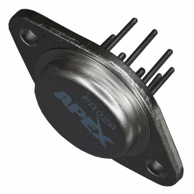
wires provide reliable interconnections at all operating temperatures. The 8-pin TO-3 package is hermetically
sealed and electrically isolated. Isolation washers are not recommended. The use of compressible thermal
washers and/or improper mounting torque will void the product warranty. Please see Application Note 1
“General Operating Considerations.”
www.apexanalog.com
© Apex Microtechnology Inc.
All rights reserved
Nov 2018
PA02U Rev U
�PA02 • PA02A
Figure 1: Equivalent Schematic
2
R1
R2
R5
R3
D1
Q1
R6
Q2
R4
Q4
6
R7
1
Q3
3
R15
A1
5
Q5
R8
Q7
R9
R10
R12
R13
4
Q6
8
R14
Q8
D2
R11
7
TYPICAL CONNECTIONS
Figure 2: Typical Connections
2
PA02U Rev U
�PA02 • PA02A
PINOUT AND DESCRIPTION TABLE
Figure 3: External Connections
Pin Number
Name
Description
1
+CL
Connect to the sourcing current limit resistor, and then the +VS pin. Power supply
current flows into this pin through RCL+.
2
+VS
The positive supply rail.
3, 4
OUT
The output. Connect this pin to load and to the feedback resistors. (Pins 3 and 4 are
internally connected).
5
-IN
The inverting input.
6
+IN
The non-inverting input.
7
-VS
The negative supply rail.
-CL
Connect to the sinking current limit resistor, and then the -VS pin. Power supply current flows out of this pin through RCL-.
8
PA02U Rev U
3
�PA02 • PA02A
SPECIFICATIONS
The power supply voltage for all specifications is the TYP rating unless otherwise noted as a test condition. Full temperature specifications are guaranteed but not 100% tested. The absolute maximum negative
input voltage is equal to the negative power supply voltage plus 1V (-VS + 1V).
ABSOLUTE MAXIMUM RATINGS
Parameter
Max
Units
+Vs to -Vs
38
V
Output Current, within SOA
IOUT
5
A
Power Dissipation, internal 1
PD
48
W
Supply Voltage, total
Input Voltage, differential
Input Voltage, common mode
Symbol
Min
VIN (Diff)
-30
30
V
VCM
-VS + 2V
+VS - 2V
V
350
°C
150
°C
-65
+150
°C
-55
+125
°C
Temperature, pin solder, 10s max.
Temperature, junction 1
TJ
Temperature Range, storage
Operating Temperature Range, case
TC
1. Long term operation at the maximum junction temperature will result in reduced product life. Derate internal power dissipation to achieve high MTTF.
CAUTION
4
The internal substrate contains beryllia (BeO). Do not break the seal. If accidentally broken, do
not crush, machine, or subject to temperatures in excess of 850°C to avoid generating toxic
fumes.
PA02U Rev U
�PA02 • PA02A
INPUT
Test
Conditions
Parameter
PA02
Min
PA02A
Typ
Max
Min
Typ
Max
Units
Offset Voltage, initial
TC = 25°C
±5
±10
±1
±3
mV
Offset Voltage vs. temperature
Full temp range
±10
±50
*
±25
µV/°C
Offset Voltage vs. supply
TC = 25°C
±10
*
µV/V
Offset Voltage vs. power
TC = 25°C
±6
*
µV/W
Bias Current, initial
TC = 25°C
50
Bias Current vs. temperature
TC = 85°C
Bias Current vs. supply
TC = 25°C
0.01
Offset Current, initial
TC = 25°C
25
Offset Current vs. temperature
TC = 85°C
Input Impedance, DC
TC = 25°C
1000
*
GΩ
Input Capacitance
TC = 25°C
3
*
pF
1
200
25
200
100
pA
*
pA/°C
*
100
15
100
pA/V
50
pA
*
pA/°C
Common Mode Voltage Range ,
Pos.
Full temp range
+VS –6 +VS –3
*
*
V
Common Mode Voltage Range 1,
Neg.
Full temp range
–VS +6 –VS +5
*
*
V
Common Mode Rejection, DC
Full temp range
*
*
dB
70
100
1. Exceeding CMV range can cause the output to latch.
GAIN
Parameter
Test
Conditions
Open Loop Gain @ 10 Hz
TC = 25°C, 1 kΩ
load
Open Loop Gain @ 10 Hz
Full temp range,
10 kΩ load
Gain Bandwidth Product @ 1 MHz
TC = 25°C, 10 Ω
load
Power Bandwidth
Phase Margin
PA02U Rev U
PA02
Min
Typ
PA02A
Max
Min
103
Typ
Max
Units
*
dB
*
dB
4.5
*
MHz
TC = 25°C, 10 Ω
load
350
*
kHz
Full temp range,
10 Ω load
30
*
°
86
100
*
5
�PA02 • PA02A
OUTPUT
Parameter
Test
Conditions
PA02
Min
Typ
PA02A
Max
Min
Typ
Max
Units
Voltage Swing 1
TC=25°C, IOUT =
5A, RCL = 0.08 Ω
±VS –4 ±VS –3
*
*
V
Voltage Swing 1
Full temp range,
±VS –2 ±VS–1.2
IOUT = 2A
*
*
V
Current, peak
TC = 25°C
*
Settling Time to 0.1%
TC=25°C, 2V step
Slew Rate
TC = 25°C
Capacitive Load
Full temp range,
AV > 10
SOA
*
Harmonic Distortion
PO=0.5W, F = 1
kHz, RL = 10 Ω
0.004
*
V
Small Signal rise/fall time
RL = 10 Ω, AV = 1
100
*
ns
Small Signal overshoot
RL = 10 Ω, AV = 1
10
*
%
5
0.6
13
20
*
A
*
µs
*
V/µs
1. +VS and –VS denote the positive and negative supply rail respectively. Total VS is measured from +VS to –VS.
POWER SUPPLY
PA02
PA02A
Test
Conditions
Min
Typ
Max
Min
Typ
Max
Voltage
Full temp range
±7
±15
±19
*
*
*
V
Current, Quiescent
TC = 25°C
27
40
*
*
mA
Parameter
Units
THERMAL
Parameter
Test
Conditions
PA02
Min
PA02A
Typ
Max
Min
Typ
Max
Units
Resistance, AC junction to case1
F > 60 Hz
1.9
2.1
*
*
°C/W
Resistance, DC junction to case
F < 60 Hz
2.4
2.6
*
*
°C/W
Resistance, junction to air
Temperature Range, case
30
Meets full range
specifications
-25
*
+85
-55
°C/W
+125
°C
1. Rating applies if the output current alternates between both output transistors at a rate faster than 60 Hz.
Note: * The specification of PA02A is identical to the specification for PA02 in applicable column to the left.
6
PA02U Rev U
�PA02 • PA02A
TYPICAL PERFORMANCE GRAPHS
Figure 4: Power Derating
Figure 5: Output Voltage Swing
3.5
^ĂƚƵƌĂƟŽŶ�sŽůƚĂŐĞ͕�sS-sOUT ;s)
/ŶƚĞƌŶĂů�WŽǁĞƌ��ŝƐƐŝƉĂƟŽŶ͕�W�;tͿ
50
40
T = TC
30
20
10
T = TA
3.0
2.5
TC�с�ϮϱΣ�ƚŽ�ϴϱΣ�
2.0
1.5
цsOUT
1.0
0.5
0
0
25
50
75
100
125
0
150
1
120
0
100
-30
80
-60
60
40
-120
-150
0
-180
-210
-20
1k
10k
0.1M 1M
Frequency, F (Hz)
PA02U Rev U
5
-90
20
100
4
Figure 7: Phase Response
Phase, ˇ�;Σ)
Open Loop Gain, AOL (dB)
Figure 6: Small Signal Response
10
3
Output Current, IOUT (A)
Temperature, T (°C)
1
2
10M
1
10
100
1k
10k
0.1M 1M
10M
&ƌĞƋƵĞŶĐLJ͕�&�;,nj)
7
�PA02 • PA02A
Figure 8: Current Limit
Figure 9: Power Response
3.0
30
| +VS | + | –VS | = 36V
Output Voltage, VOUT (VP-P)
Current Limit, ICL (A)
2.5
RCL�с�Ϭ͘ϯ�ɏ
2.0
1.5
RCL�с�Ϭ͘ϲϮ�ɏ
1.0
0.5
0
-25
23
18
| +VS | + | –VS | = 30V
13
10
7.8
0
25
50
75
100
6
0.1M
125
0.2M
Case Temperature, TC (°C)
Figure 11: Common Mode Rejection
120
�ŽŵŵŽŶ�DŽĚĞ�ZĞũĞĐƟŽŶ͕��DZ�;Ě�Ϳ
Normalized Bias Current, IB (X)
256
64
16
4
1
0.25
100
80
60
40
20
5
25
45
65
85
Case Temperature, TC (°C)
8
0.5M 0.7M 1M
Frequency, F (Hz)
Figure 10: Bias Current
0.06
-15
0.3M
105
1
10
100
1k
10k
0.1M 1M
10M
Frequency, F (Hz)
PA02U Rev U
�PA02 • PA02A
Figure 12: Power Supply Rejection
Figure 13: Input Noise
40
Input Noise Voltage, en (Ŷsͬя,nj)
WŽǁĞƌ�^ƵƉƉůLJ�ZĞũĞĐƟŽŶ͕�W^Z�;Ě�Ϳ
140
120
100
+VS
80
60
–VS
40
20
0
10
100
1k
10k
0.1M
1M
35
30
25
20
15
10
10M
10
100
Frequency, F (Hz)
Figure 15: Settling Time
1.6
3
1.5
2.5
AD
1.4
Time, t (μs)
2
1.3
1.2
NO
LO
1.5
AD
V
LO
NO
10m
�
Ϭ�ɏ�>K�
ϭϬŵs��ϭ
.5
1.0
0
0
25
50
75
100
Case Temperature, TC (°C)
PA02U Rev U
V
1m
1
1.1
0.9
-25
0.1M
10k
Frequency, F (Hz)
Figure 14: Quiescent Current
Normal Quiescent Current, IQ (X)
1k
125
1
2
3
4
5
6
7
8
Output Change From Zero (V)
9
�PA02 • PA02A
Figure 16: Harmonic Distortion
Figure 17: Pulse Response
15
1
Output Voltage,VOUT (V)
�ŝƐƚŽƌƟŽŶ͕�d,��;йͿ
0.3
Gain = 1
>ŽĂĚ�с�ϭϬ�ɏ
0.1
W
m
0
=5
0.03
PO
5W
.
=0
0.01
PO
P O=
0.003
0.001
100
5W
VIN = ±1V, tr = 100ns
>ŽĂĚ�с�ϭϬ�ɏ���
10
5
0
-5
-10
-15
300
1k
3k
10k
0
0.1M 0.3M
30k
1
2
3
4
5
Time, t (μs)
Frequency, F (Hz)
Figure 18: Pulse Response
Figure 19: Loading Effects
0.3
0
�ĞůƚĂ�'ĂŝŶ�tŝƚŚ�>ŽĂĚ͕�ѐ� (dB)
Output Voltage,VOUT (V)
VIN = ±0.2V, tr = 50ns
0.2
0.1
0
-0.1
-0.2
-0.3
0
0.5
1.0
Time, t (μs)
10
1.5
-0.3
IOUT�с�ϭϱϬŵ�
-0.6
-0.9
IOUT�с�ϰϬϬŵ�
-1.2
-1.5
100
1k
10k
0.1M
Frequency, F (Hz)
PA02U Rev U
�PA02 • PA02A
SAFE OPERATING AREA (SOA)
The SOA curves combine the effect of all limits for this Power Op Amp. For a given application, the direction and magnitude of the output current should be calculated or measured and checked against the SOA
curves. This is simple for resistive loads but more complex for reactive and EMF generating loads. The following guidelines may save extensive analytical efforts:
1. Under transient conditions, capacitive and dynamic* loads up to the following maximums are safe:
CAPACITIVE LOAD
INDUCTIVE LOAD
±VS
ICL = 5A
ICL = 2A
ICL = 5A
ICL = 2A
18V
2 mF
0.7 mF
0.2 H
10 mH
15V
10 mF
2.2 mF
0.7 H
25 mH
10V
25 mF
10 mF
5H
50 mH
* If the inductive load is driven near steady state conditions, allowing the output voltage to drop
more than 8V below the supply rail with ICL = 5A, or 17V below the supply rail with ICL = 2A while
the amplifier is current limiting, the inductor should be capacitively coupled or the current limit must
be lowered to meet SOA criteria.
2. The amplifier can handle any EMF generating or reactive load and short circuits to the supply rails or
shorts to common if the current limits are set as follows at TC = 85°C.
±VS
Short to ±VS
C, L, or EMF Load
Short to Common
18V
0.5A
1.7A
15V
0.7A
2.8A
10V
1.6A
4.2A
These simplified limits may be exceeded with further analysis using the operating conditions for a
specific application.
5.0
4.0
T
TĐ Đ = 25
TĐ
°C
=
= 1 70
TĐ
°
C
00
=1
°C
25
°C
3.0
2.0
Ɛ
�ϱŵ
ƚ�с ŽŶĚ ǁŶ
Đ
^Ğ ĂŬĚŽ
Ğ
�ƌ
1.5
Ğ
ƚĂƚ
LJ�^
ĂĚ
^ƚĞ
KƵƚƉƵƚ��ƵƌƌĞŶƚ�&ƌŽŵ�нVS�Žƌ�ͲVS (A)
Figure 20: SOA
1.0
0.7
dŚ
Ğƌ
0.5
ŵ
Ăů
0.3
0.2
2
3
5
7
10
15 20 25 30 40
^ƵƉƉůLJ�ƚŽ�KƵƚƉƵƚ��ŝīĞƌĞŶƟĂů͕�VS-VOUT (V)
PA02U Rev U
11
�PA02 • PA02A
GENERAL
Please read Application Note 1 “General Operating Considerations” which covers stability, supplies, heat
sinking, mounting, current limit, SOA interpretation, and specification interpretation. Visit www.apexanalog.com for Apex Microtechnology’s complete Application Notes library, Technical Seminar Workbook, and
Evaluation Kits.
TYPICAL APPLICATION
LOW INTERNAL LOSS MAXIMIZES EFFICIENCY
When system voltages are low and power is at a premium, the PA02 is a natural choice. The circuit below
utilizes not only the feature of low internal loss of the PA02, but also its very low distortion level to implement a crystal clear audio amplifier suitable even for airborne applications. This circuit uses AC coupling of
both the input signal and the gain circuit to render DC voltage across the speaker insignificant. The resistor
and capacitor across the inputs form a stability enhancement network. The 0.27 Ω current limit resistors provide protection in the event of an output short circuit.
Figure 21: Typical Application (Vehicular Sound System Power Stage)
12
PA02U Rev U
�PA02 • PA02A
CURRENT LIMIT
Proper operation requires the use of two current limit resistors, connected as shown in the external connection diagram. The minimum value for RCL is 0.12 Ω, however for optimum reliability it should be set as
high as possible.
0.65VR CL = ---------------I CL A
Where:
ICL is the current limit in Amperes.
RCL is the current limit resistor value in Ohms.
Refer to Application Note 1 “General Operating Considerations” section of the handbook for current limit
adjust details.
DEVICE MOUNTING
The case (mounting flange) is electrically isolated and should be mounted directly to a heatsink with thermal compound. Screws with Belville spring washers are recommended to maintain positive clamping pressure on heatsink mounting surfaces. Long periods of thermal cycling can loosen mounting screws and
increase thermal resistance.
Since the case is electrically isolated (floating) with respect to the internal circuits it is recommended to connect it to common or other convenient AC ground potential.
PA02U Rev U
13
�PA02 • PA02A
PACKAGE OPTIONS
PACKAGE STYLE CE
14
PA02U Rev U
�PA02 • PA02A
NEED TECHNICAL HELP? CONTACT APEX SUPPORT!
For all Apex Microtechnology product questions and inquiries, call toll free 800-546-2739 in North America. For
inquiries via email, please contact apex.support@apexanalog.com. International customers can also request
support by contacting their local Apex Microtechnology Sales Representative. To find the one nearest to you,
go to www.apexanalog.com
IMPORTANT NOTICE
Apex Microtechnology, Inc. has made every effort to insure the accuracy of the content contained in this document. However, the information is
subject to change without notice and is provided "AS IS" without warranty of any kind (expressed or implied). Apex Microtechnology reserves the right
to make changes without further notice to any specifications or products mentioned herein to improve reliability. This document is the property of
Apex Microtechnology and by furnishing this information, Apex Microtechnology grants no license, expressed or implied under any patents, mask
work rights, copyrights, trademarks, trade secrets or other intellectual property rights. Apex Microtechnology owns the copyrights associated with the
information contained herein and gives consent for copies to be made of the information only for use within your organization with respect to Apex
Microtechnology integrated circuits or other products of Apex Microtechnology. This consent does not extend to other copying such as copying for
general distribution, advertising or promotional purposes, or for creating any work for resale.
APEX MICROTECHNOLOGY PRODUCTS ARE NOT DESIGNED, AUTHORIZED OR WARRANTED TO BE SUITABLE FOR USE IN PRODUCTS USED FOR LIFE
SUPPORT, AUTOMOTIVE SAFETY, SECURITY DEVICES, OR OTHER CRITICAL APPLICATIONS. PRODUCTS IN SUCH APPLICATIONS ARE UNDERSTOOD TO BE
FULLY AT THE CUSTOMER OR THE CUSTOMER’S RISK.
Apex Microtechnology, Apex and Apex Precision Power are trademarks of Apex Microtechnology, Inc. All other corporate names noted herein may be
trademarks of their respective holders.
PA02U Rev U
15
�


 工商网监
湘ICP备2023018690号
工商网监
湘ICP备2023018690号
