SA08
SA08
P r o d uSA08
c t IInnnnoovvaa t i o n FFr roomm
Pulse Width Modulation Amplifiers
FEATURES
• IGBT OUTPUTS
• WIDE SUPPLY RANGE—16-450V
• 20A TO 100°C case
• 3 PROTECTION CIRCUITS
• SYNCHRONIZED OR EXTERNAL OSCILLATOR
• FLEXIBLE FREQUENCY CONTROL
APPLICATIONS
• MOTORS
• REACTIVE LOADS
• MAGNETIC BEARINGS
• LARGE PIEZO ELEMENTS
• OFF-LINE DRIVERS
• C-D WELD CONTROLLER
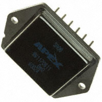
12-pin Power DIP
PACKAGE STYLE CR
EXTERNAL CONNECTIONS
DESCRIPTION
ISENSE A
The SA08 is a pulse width modulation amplifier that can
supply 9KW to the load. An internal oscillator requires no
external components. The clock input stage divides the oscillator frequency by two, which provides the switching frequency
of 22.5 kHz. The oscillator may also be used to synchronize
multiple amplifiers. Current sensing is provided for each half
of the bridge giving amplitude and direction data. A shutdown
input turns off all four drivers of the H-bridge output. A high
side current limit and the programmable low side current limit
protect the amplifier from shorts to supply or ground in addition
to load shorts. The H-bridge output IGBTs are protected from
thermal overloads by directly sensing the temperature of the
die. The 12-pin hermetic MO-127 power package occupies
only 3 square inches of board space.
BLOCK DIAGRAM AND TYPICAL APPLICATION
MOTOR TORQUE CONTROL
FLAG
GND
3
2
11
3
TOP
VIEW
4
A OUT
* VCC
10
*
9
5
8
6
7
+VS
B OUT
I SENSE B
Case tied to pin 5. Allow no current in case. Bypassing of supplies
is required. Package is Apex MO-127 (STD). See Outline
Dimensions/Packages in Apex data book.
9
+VS
PWM
4
470pF
B OUT
45K
OUTPUT
DRIVERS
OSC
8
MOTOR
11
A OUT
CLK OUT
2
12
ILIM/SHDN
CURRENT
LIMIT
+PWM
CONTROL
SIGNAL
1
*See text. As +PWM goes more positive, A OUT duty cycle
increases.
Vcc
10
FLAG
CLK IN
CLK OUT
+PWM
÷2
1K
I SENSE A
SHUTDOWN
CONTROL
CLK IN
1
5V
12
5K
6
ILIM/SHDN
5
.01µF
RSENSE
1K
7
GND
I SENSE B
RSENSE
5V
SA08U
http://www.cirrus.com
Copyright © Cirrus Logic, Inc. 2009
(All Rights Reserved)
MAY 20091
APEX − SA08UREVF
�SA08
P r o d u c t I n n o v a t i o nF r o m
ABSOLUTE MAXIMUM RATINGS
SUPPLY VOLTAGE, +VS
SUPPLY VOLTAGE, VCC
POWER DISSIPATION, internal1
TEMPERATURE, pin solder - 10s
TEMPERATURE, junction2
TEMPERATURE, storage
OPERATING TEMPERATURE RANGE, case
INPUT VOLTAGE, +PWM
INPUT VOLTAGE, ILIM
SPECIFICATIONS
PARAMETER
TEST CONDITIONS2
CLOCK (CLK)
CLK OUT, high level4
CLK OUT, low level4
CLK IN, low level4
CLK IN, high level4
FREQUENCY
ANALOG INPUT (+PWM)
center voltage
P-P voltage
FLAG
FLAG, high level
FLAG, low level
OUTPUT
TOTAL DROP
EFFICIENCY, 20A output
SWITCHING FREQUENCY
CURRENT, continuous4
CURRENT, peak4
POWER SUPPLY
VOLTAGE, VS
VOLTAGE, VCC
CURRENT, VCC
CURRENT, VCC, shutdown
CURRENT, VS
IOUT ≤ 1mA
IOUT ≤ 1mA
MIN
4.8
0
0
3.7
44.10
0/100% modulation
I = 20A
VS = 380V
OSC in ÷ 2
100°C case
Full temperature range
Full temperature range
IOUT = 0
22.05
20
28
165
14
450V
16V
250W
300°C
150°C
–65 to +150°C
–55 to +125°C
0 TO +11V
0 TO +10V
TYP
MAX
UNITS
45.00
5.3
.4
.9
5.4
46.90
V
V
V
V
kHz
5
4
V
V
10
0
V
V
5.4
22.95
V
%
kHz
A
A
450
16
80
50
90
V
V
mA
mA
mA
110
100
mV
nA
1
+85
°C/W
°C/W
°C
98
22.50
240
15
No Load
ILIM/SHUTDOWN
TRIP POINT
INPUT CURRENT
90
THERMAL3
RESISTANCE, junction to case
RESISTANCE, junction to air
TEMPERATURE RANGE, case
Full temperature range, for each die
Full temperature range
Meets full range specifications
12
–25
NOTES: 1. Each of the two active output transistors can dissipate 125W.
2. Unless otherwise noted: TC = 25°C, VS, VCC at typical specification.
3. Long term operation at the maximum junction temperature will result in reduced product life. Derate internal power dissipation to achieve high MTTF. For guidance, refer to the heatsink data sheet.
4. Guaranteed but not tested.
5. If 100% duty cycle is not required VS(MIN) = 0V.
CAUTION
2
The SA08 is constructed from static sensitive components. ESD handling procedures must be observed.
The internal substrate contains beryllia (BeO). Do not break the seal. If accidentally broken, do not crush,
machine, or subject to temperatures in excess of 850°C to avoid generating toxic fumes.
SA08U
�SA08
P r o d u c t I n n o v a t i o nF r o m
75
50
0
EACH ACTIVE
OUTPUT TRANSISTOR
0
20
75
100
25
50
CASE TEMPERATURE, (°C)
102.0
NORMALIZED FREQUENCY, (%)
100
25
CLOCK FREQUENCY OVER TEMP
CLOCK LOADING
100
NORMALIZED FREQUENCY, (%)
INTERNAL POWER DISSIPATION, (W)
POWER DERATING
125
99
98
97
96
F NOMINAL = 45kHz
95
125
101.5
101.0
100.5
99.5
99.0
98.5
98.0
100K
1M
10K
CLOCK LOAD RESISTANCE, (Ω)
REVERSE DIODE
100
–50 –25 0
25 50 75 100 125
CASE TEMPERATURE, (°C)
TOTAL VOLTAGE DROP
6
TOTAL VOLTAGE DROP, (V)
12
Tc = 25°C
4
100°C
3
2
0
1.0
1.5
2.0
2.5
3.0
0.5
DIODE FORWARD VOLTAGE DROP, (V)
20
25°C
4
0
4
8
12
16
OUTPUT CURRENT, I (A)
20
DUTY CYCLE VS ANALOG INPUT
CONTINUOUS AMPS
100
DUTY CYCLE, (%)
CONTINUOUS AMPS, (A)
B OUT
80
18
16
14
60
40
20
12
A OUT
115
110
50
75
100
CASE TEMPERATURE, (°C)
125
Vcc QUIESCENT CURRENT
Vcc = 15V
F = 22.5 kHz
105
100
NORMAL
OPERATION
95
90
85
80
SA08U
0
SHUTDOWN
OPERATION
–50 –25 0
25 50 75 100 125
CASE TEMPERATURE, (°C)
NORMALIZED Vs QUIESCENT CURRENT, (%)
NORMALIZED Vcc QUIESCENT CURRENT, (%)
10
25
3
150
4
5
6
ANALOG INPUT, (V)
7
100
75
50
0
100
100
Vs QUIESCENT VS VOLTAGE
125
100
200
300
Vs, (V)
400
500
Vcc QUIESCENT CURRENT
NORMALIZED QUIESCENT CURRENT, (%)
Tc = 100°C
8
5
NORMALIZED Vs QUIESCENT CURRENT, (%)
FORWARD CURRENT, (A)
CASE TEMPERATURE
16
96
92
88
84
5
10
15
20
25
SWITCHING FREQUENCY, F (kHz)
Vs QUIESCENT VS FREQUENCY
90
80
70
60
50
5
10
15
20
25
SWITCHING FREQUENCY, F (kHz)
3
�SA08
P r o d u c t I n n o v a t i o nF r o m
GENERAL
Please read Application Note 30 on "PWM Basics". Refer
to Application Note 1 "General Operating Considerations" for
helpful information regarding power supplies, heat sinking
and mounting. Visit www.Cirrus.com for design tools that help
automate pwm filter design; heat sink selection; Apex Precision
Power’s complete Application Notes library; Technical Seminar
Workbook; and Evaluation Kits.
CLOCK CIRCUIT AND RAMP GENERATOR
The clock frequency is internally set to a frequency of approximately 45kHz. The CLK OUT pin will normally be tied to
the CLK IN pin. The clock is divided by two and applied to an
RC network which produces a ramp signal. An external clock
signal can be applied to the CLK IN pin for synchronization
purposes, but must be 45 kHz +/- 2%.
FLAG OUTPUT
Whenever the SA08 has detected a fault condition, the flag
output is set high (10V). When the programmable low side
current limit is exceeded, the FLAG output will be set high.
The FLAG output will be reset low on the next clock cycle. This
reflects the pulse-by-pulse current limiting feature. When the
internally-set high side current limit is tripped or the thermal
limit is reached, the FLAG output is latched high. See PROTECTION CIRCUITS below.
PROTECTION CIRCUITS
A fixed internal current limit senses the high side current.
Should either of the outputs be shorted to ground the high side
current limit will latch off the output transistors. The temperature
of the output transistors is also monitored. Should a fault condition raise the temperature of the output transistors to 165°C
the thermal protection circuit latch off the output transistors.
The latched condition can be cleared by either recycling the
Vcc power or by toggling the I LIMIT/SHDN input with a 10V
pulse. See Figures A and B. The outputs will remain off as long
as the shutdown pulse is high (10V).
CURRENT LIMIT
There are two load current sensing pins, I SENSE A and I
SENSE B. The two pins can be shorted in the voltage mode
connection but both must be used in the current mode connection (see figures A and B). It is recommended that RLIMIT resistors
be non-inductive. Load current flows in the I SENSE pins. To
avoid errors due to lead lengths connect the I LIMIT/SHDN pin
directly to the RLIMIT resistors (through the filter network and
shutdown divider resisI SENSE A
tor) and connect the
RLIMIT resistors directly
R LIMIT
to the GND pin.
I SENSE B
Sw i t c h i n g n o i s e
spikes will invariably
5K SHUTDOWN
be found at the I SENSE I LIMIT/SHDN R FILTER
SIGNAL
pins. The noise spikes
0/10V
C FILTER
1N4148
could trip the current
limit threshold which
is only 100 mV. RFILTER FIGURE A. CURRENT LIMIT WITH
and CFILTER should be SHUTDOWN VOLTAGE MODE.
4
adjusted so as to
reduce the switching noise well below
100 mV to prevent
R LIMIT
false current limitI SENSE B
5K
ing. The sum of the
DC level plus the
R LIMIT
noise peak will determine the current
SHUTDOWN
limiting value. As
I LIMIT/SHDN R
SIGNAL
FILTER
in most switching
0/10V
circuits it may be
C FILTER
1N4148
difficult to determine the true noise
FIGURE B. CURRENT LIMIT WITH
amplitude without
SHUTDOWN CURRENT MODE.
careful attention to
grounding of the oscilloscope probe. Use the shortest possible
ground lead for the probe and connect exactly at the GND
terminal of the amplifier. Suggested starting values are CFILTER
= .1uF, RFILTER = 5k .
I SENSE A
5K
The required value of RLIMIT in voltage mode may be calculated by:
RLIMIT = .1 V / ILIMIT
where RLIMIT is the required resistor value, and ILIMIT is the
maximum desired current. In current mode the required value
of each RLIMIT is 2 times this value since the sense voltage is
divided down by 2 (see Figure B). If RSHDN is used it will further
divide down the sense voltage. The shutdown divider network
will also have an effect on the filtering circuit.
BYPASSING
Adequate bypassing of the power supplies is required for
proper operation. Failure to do so can cause erratic and low
efficiency operation as well as excessive ringing at the outputs. The Vs supply should be bypassed with at least a 1µF
ceramic capacitor in parallel with another low ESR capacitor
of at least 10µF per amp of output current. Capacitor types
rated for switching applications are the only types that should
be considered. The bypass capacitors must be physically
connected directly to the power supply pins. Even one inch of
lead length will cause excessive ringing at the outputs. This
is due to the very fast switching times and the inductance of
the lead connection. The bypassing requirements of the Vcc
supply are less stringent, but still necessary. A .1µF to .47µF
ceramic capacitor connected directly to the Vcc pin will suffice.
STARTUP CONDITIONS
The high side of the IGBT output bridge circuit is driven by
bootstrap circuit and charge pump arrangement. In order for
the circuit to produce a 100% duty cycle indefinitely the low
side of each half bridge circuit must have previously been in
the ON condition. This means, in turn, that if the input signal
to the SA08 at startup is demanding a 100% duty cycle, the
output may not follow the command and may be in a tri-state
condition. The ramp signal must cross the input signal at some
point to correctly determine the output state. After the ramp
crosses the input signal level one time, the output state will
be correct thereafter.
SA08U
�P r o d u c t I n n o v a t i o nF r o m
SA08
Contacting Cirrus Logic Support
For all Apex Precision Power product questions and inquiries, call toll free 800-546-2739 in North America.
For inquiries via email, please contact apex.support@cirrus.com.
International customers can also request support by contacting their local Cirrus Logic Sales Representative.
To find the one nearest to you, go to www.cirrus.com
IMPORTANT NOTICE
Cirrus Logic, Inc. and its subsidiaries ("Cirrus") believe that the information contained in this document is accurate and reliable. However, the information is subject
to change without notice and is provided "AS IS" without warranty of any kind (express or implied). Customers are advised to obtain the latest version of relevant
information to verify, before placing orders, that information being relied on is current and complete. All products are sold subject to the terms and conditions of sale
supplied at the time of order acknowledgment, including those pertaining to warranty, indemnification, and limitation of liability. No responsibility is assumed by Cirrus
for the use of this information, including use of this information as the basis for manufacture or sale of any items, or for infringement of patents or other rights of third
parties. This document is the property of Cirrus and by furnishing this information, Cirrus grants no license, express or implied under any patents, mask work rights,
copyrights, trademarks, trade secrets or other intellectual property rights. Cirrus owns the copyrights associated with the information contained herein and gives consent for copies to be made of the information only for use within your organization with respect to Cirrus integrated circuits or other products of Cirrus. This consent
does not extend to other copying such as copying for general distribution, advertising or promotional purposes, or for creating any work for resale.
CERTAIN APPLICATIONS USING SEMICONDUCTOR PRODUCTS MAY INVOLVE POTENTIAL RISKS OF DEATH, PERSONAL INJURY, OR SEVERE PROPERTY OR ENVIRONMENTAL DAMAGE (“CRITICAL APPLICATIONS”). CIRRUS PRODUCTS ARE NOT DESIGNED, AUTHORIZED OR WARRANTED TO BE
SUITABLE FOR USE IN PRODUCTS SURGICALLY IMPLANTED INTO THE BODY, AUTOMOTIVE SAFETY OR SECURITY DEVICES, LIFE SUPPORT PRODUCTS OR OTHER CRITICAL APPLICATIONS. INCLUSION OF CIRRUS PRODUCTS IN SUCH APPLICATIONS IS UNDERSTOOD TO BE FULLY AT THE CUSTOMER’S RISK AND CIRRUS DISCLAIMS AND MAKES NO WARRANTY, EXPRESS, STATUTORY OR IMPLIED, INCLUDING THE IMPLIED WARRANTIES OF
MERCHANTABILITY AND FITNESS FOR PARTICULAR PURPOSE, WITH REGARD TO ANY CIRRUS PRODUCT THAT IS USED IN SUCH A MANNER. IF THE
CUSTOMER OR CUSTOMER’S CUSTOMER USES OR PERMITS THE USE OF CIRRUS PRODUCTS IN CRITICAL APPLICATIONS, CUSTOMER AGREES,
BY SUCH USE, TO FULLY INDEMNIFY CIRRUS, ITS OFFICERS, DIRECTORS, EMPLOYEES, DISTRIBUTORS AND OTHER AGENTS FROM ANY AND ALL
LIABILITY, INCLUDING ATTORNEYS’ FEES AND COSTS, THAT MAY RESULT FROM OR ARISE IN CONNECTION WITH THESE USES.
Cirrus Logic, Cirrus, and the Cirrus Logic logo designs, Apex Precision Power, Apex and the Apex Precision Power logo designs are trademarks of Cirrus Logic, Inc.
All other brand and product names in this document may be trademarks or service marks of their respective owners.
SA08U
5
�


 工商网监
湘ICP备2023018690号
工商网监
湘ICP备2023018690号
