SWR200
RoHS
Precision Sine Wave Reference
COMPLIANT
FEATURES
•
•
•
•
•
•
Very High Accuracy: +7.071Vrms ±0.5%
Extremely Low Drift: 20ppm/°C
(-55°C to +125°C)
Excellent Stability: 10ppm/1000 Hrs. Typical
Low Distortion: 0.1%THD @ F = 3300 Hz
Hermetic 14-pin Ceramic DIP
Military Processing Option
APPLICATIONS
•
•
•
•
•
•
Transducer Excitation
High Resolution Servo Systems
High Precision Test and Measurement Instruments
AC Voltage Standard
LVDT or RVDT Reference
Multiplying D/A Reference
DESCRIPTION
SWR200 is a Precision Sine Wave Reference providing an ultra stable sine wave output of +7.071V at
±0.5% initial accuracy and temperature coefficient as low as 20ppm/°C over the full military temperature
range. The extreme accuracy is made possible by a chopper-based AGC circuit. The temperature characteristic of the chopper circuit compensates the typical nonlinearity of the internal DC Zener reference, resulting in
a nearly linear amplitude-temperature characteristic. Frequency of the SWR200 is programmable with
two external capacitors.
The SWR200 is available in a 14-pin bottom braze package. They are hermetically sealed and “M” versions are screened for high reliability and quality.
SWR200 is well suited for any application requiring a stable sine wave source. The SWR200 can be used as
a reference source in precision sensing systems based on LVDT or RVDT position sensors. A programmable AC
reference can be constructed using the SWR200 as a reference for a high accuracy multiplying Digital to Analog Converter.
SELECTION GUIDE
Output (TYP)
Temperature
Operating
Range
Package
SWR200C
+7.071V
-25°C to +85°C
DIP
SWR200M
+7.071V
-55°C to +125°C
DIP
Type
www.apexanalog.com
© Apex Microtechnology Inc.
All rights reserved
Dec 2018
SWR200DS Rev L
�SWR200
TYPICAL CONNECTION
Figure 1: Typical Connection
PIN DESCRIPTIONS
2
Pin Number
Name
Description
1, 2
C1
Frequency selection capacitor connection C1. See applicable selection.
3
-VPS
The negative supply voltage connection.
7
GND
Ground.
8
REF_GND
Provided for accurate ground sensing. Internally connected to GND.
9
OUT
The output.
12
+VPS
The positive supply voltage connection.
13, 14
C2
Frequency selection capacitor connection C2. See applicable selection.
4
C3
Optional frequency range expansion. Connect C3 between pins 4 and 5 of value
approximately 2 x C1.
5
Extended Range
Connection
Optional frequency range expansion. See Typical Application drawing for connection.
6
C4
Optional frequency range expansion. Connect C4 between pins 5 and 6 of value
approximately 20 x C2.
10, 11
NC
No connection.
SWR200DS Rev L
�SWR200
SPECIFICATIONS
VPS = ±15V, T = 25°C, RL = 10 kΩ unless otherwise noted.
ABSOLUTE MAXIMUM RATINGS
SWR200C
Parameter
Power Supply
SWR200M
Units
Min
Typ
Max
Min
Typ
Max
±13.5
±15
±22
*
*
*
V
+85
-55
+125
°C
+85
*
*
°C
*
°C
Operating Temperature
-25
Storage Temperature
-65
Short Circuit Protection
Continuous
Soldering Temperature (10 sec max)
*
+260
ELECTRICAL SPECIFICATIONS
SWR200C
Parameter1
Min
Output Voltage
Typ
SWR200M
Max
Min
7.071
Initial Error
Typ
*
±0.5
Warmup Drift
100
DC Offset
3
TMIN - TMAX 2
18
*
20.0
Long-Term Stability
10
Output Current
Load Regulation
Power Supply Current, +PS
3
Power Supply Current, -PS 3
Power Supply Current, Distortion
Normalized Error
%
*
mV
*
µV/°C
30.0
ppm/ °C
µV
ppm/°C
10
*
ppm/V
3
*
ppm/mA
*
mA
10.5
13
*
*
mA
9.5
13
*
*
mA
*
%
*
Hz
*
Hz
*
ppm/°C
3
0.5
0.98
*
*
±10
Line Regulation
Units
V
*
3
DC Offset Over Temp.
Max
1
1.02
*
10 k
*
*
–5
Range (f)
f
----f
10 f = ---------------C1 C2
vs. Temperature
400
15
1. Pin 8 is internally connected to Pin 7 and can be used as Ref. GND.
2. Using the Box Method, the specified value is the maximum deviation from the output voltage at 25°C over the specified
operating temperature range.
3. The specified values are unloaded.
Note: Same as C Models
SWR200DS Rev L
3
�SWR200
TYPICAL PERFORMANCE GRAPHS
Figure 2: VOUT vs. Temperature
(SWR200C)
15.6
0
-15.6
-50 -25
0
25
0
-35
-50
Lower Limit
-20
50
75
Lower Limit
-50 -25 0
100 125
Figure 4: % Δ Freq. vs. Temperature
(SWR200C)
Figure 5: % Δ Freq. vs. Temperature
(SWR200M)
0.5
0.5
Upper Limit
Upper Limit
ѐF/F (%)
0.1
0
-0.1
0.2
0
-0.2
Lower Limit
Lower Limit
-0.5
-0.5
-50 -25
0
25
50
75
Temperature (°C)
4
25 50 75 100 125
Temperature (°C)
Temperature (°C)
ѐF/F (%)
Upper Limit
50
35
Upper Limit
ѐVOUT(mV)
ѐVOUT (mV)
20
Figure 3: VOUT vs. Temperature
(SWR200M)
100 125
-50 -25
0
25 50
75
100 125
Temperature (°C)
SWR200DS Rev L
�SWR200
Figure 7: Distortion vs. Frequency
0.4
2.00
0.3
1.50
�ŝƐƚŽƌƟŽŶ�;й)
�ŝƐƚŽƌƟŽŶ�;й)
Figure 6: Distortion vs. Temperature
0.2
0.1
1.00
0.50
0
-50
0
50
0
100
1k
Temperature (°C)
100k
Frequency (Hz)
Figure 8: Normalized Distortion vs.
C2/C1
Figure 9: Power Supply Current vs.
Temperature
10.0
15
12
1.0
Current (mA)
EŽƌŵĂůŝnjĞĚ��ŝƐƚŽƌƟŽŶ
10k
0.1
+PS
9
-PS
6
0
0.8
0.9
1.0
1.1
C2/C1
SWR200DS Rev L
1.2
1.3
1.4
3
-50
0
50
100
Temperature (°C)
5
�SWR200
Figure 10: Case Temp. Rise Above Ambient
vs. Output Current
Figure 11: Junction Temp. Rise Above Case
Temp. vs. Output Current
25
ZŝƐĞ�ŝŶ�:ƵŶĐƟŽŶ�Temperature (°C)
Rise in Case Temperature (°C)
20
15
10
5
0
0
2
4
6
Output Current (mA)
6
8
10
20
15
=
V CC
10
5
0
2
4
5V
±1
6
8
10
Output Current (mA)
SWR200DS Rev L
�SWR200
BLOCK DIAGRAM
Figure 12: Block Diagram
THEORY OF OPERATION
The following refers to the schematic in Figure 12. A1 and A2 are connected as a phase-shift oscillator circuit with the frequency set by the external capacitors C1 and C2. Q4 is included in the feedback loop of A1 as
a gain control element.
The oscillator output is fed to the chopper amplifier which develops an absolute value representation of
the oscillator output. The chopper output is compared to a precision DC reference in integrator amplifier A3.
This DC error signal is used to control the gain setting FET Q4.
As in all precision Zener based DC references, the drift of the Zener becomes nonlinear at temperature
extremes. The chopper amplifier drift characteristic is complementary to this nonlinearity and compensates
for the reference drift.
SWR200DS Rev L
7
�SWR200
APPLICATION INFORMATION
Figure 2 shows the connections for the SWR200 including the two frequency setting capacitors. The frequency is:
–5
10 f = ---------------C1 C2
The frequency stability is directly related to the stability of the capacitors, therefore stable capacitors like
NPO ceramic, polycarbonate or polypropylene film should be used. Specified device operation relies on the
tight matching of capacitors C1 and C2. The capacitor mismatch must not exceed 10% over the entire operating temperature range. The recommended capacitor tolerance is 5% or less to ensure specified electrical performance.
Two separate ground pins are provided for accurate ground sensing. This minimizes errors due to drops
in the ground pin which can become a significant source of error in sockets.
The offset of the SWR200 is fully specified for initial offset and drift and is low enough that it can normally
be neglected. In applications which are especially sensitive to offset the output can be AC coupled. Proper
capacitor sizing and high impedance sensing will minimize errors due to capacitive coupling.
PIN CONFIGURATION
Figure 13: Pin Configuration
8
SWR200DS Rev L
�SWR200
EXTENDED FREQUENCY RANGE
The SWR200 with two external frequency setting capacitors is fully specified for operation from 400 Hz to
10 kHz. At lower frequencies, the limitations occurs in the AGC circuit that provides the high amplitude stability of the SWR200. There is also a slight increase in distortion from 1500 Hz down to 400 Hz, which continues
as frequency decreases.
Two external capacitors (C3 and C4 in figure 14) can increase the time constant of the AGC circuit allowing for use at lower frequencies. This increase in time constant comes with the trade-off of a longer settling
time from power on.
The value for the lower frequency AGC capacitors is given by the following schematic and formula. To
predict AGC settling requirements, use the following formula:
300
--------- = T
F
Where: F is frequency in Hertz
T is time in seconds
Use of the external AGC capacitors can also have an effect on distortion. The SWR200 data sheet shows
an increasing distortion with decreasing frequency starting at 1500 Hz. This effect is entirely due to time constants within the AGC circuitry which are correctable with the inclusion of C3 and C4.
Among the application possibilities provided by frequency range enhancement of the SWR200, mention
should be made of the use of the SWR200 as an ultra-precise 60 Hz source. This can have wide application in
60 Hz testing and generation.
Figure 14: Extended Frequency External Connections
SWR200DS Rev L
9
�SWR200
PACKAGE OPTIONS
Part Number
Apex Package Style
Description
SWR200C
HC
Hermetic 14-pin Ceramic DIP
SWR200M
HC
Hermetic 14-pin Ceramic DIP
PACKAGE STYLE HC
10
SWR200DS Rev L
�SWR200
NEED TECHNICAL HELP? CONTACT APEX SUPPORT!
For all Apex Microtechnology product questions and inquiries, call toll free 800-546-2739 in North America. For
inquiries via email, please contact apex.support@apexanalog.com. International customers can also request
support by contacting their local Apex Microtechnology Sales Representative. To find the one nearest to you,
go to www.apexanalog.com
IMPORTANT NOTICE
Apex Microtechnology, Inc. has made every effort to insure the accuracy of the content contained in this document. However, the information is
subject to change without notice and is provided "AS IS" without warranty of any kind (expressed or implied). Apex Microtechnology reserves the right
to make changes without further notice to any specifications or products mentioned herein to improve reliability. This document is the property of
Apex Microtechnology and by furnishing this information, Apex Microtechnology grants no license, expressed or implied under any patents, mask
work rights, copyrights, trademarks, trade secrets or other intellectual property rights. Apex Microtechnology owns the copyrights associated with the
information contained herein and gives consent for copies to be made of the information only for use within your organization with respect to Apex
Microtechnology integrated circuits or other products of Apex Microtechnology. This consent does not extend to other copying such as copying for
general distribution, advertising or promotional purposes, or for creating any work for resale.
APEX MICROTECHNOLOGY PRODUCTS ARE NOT DESIGNED, AUTHORIZED OR WARRANTED TO BE SUITABLE FOR USE IN PRODUCTS USED FOR LIFE
SUPPORT, AUTOMOTIVE SAFETY, SECURITY DEVICES, OR OTHER CRITICAL APPLICATIONS. PRODUCTS IN SUCH APPLICATIONS ARE UNDERSTOOD TO BE
FULLY AT THE CUSTOMER OR THE CUSTOMER’S RISK.
Apex Microtechnology, Apex and Apex Precision Power are trademarks of Apex Microtechnology, Inc. All other corporate names noted herein may be
trademarks of their respective holders.
SWR200DS Rev L
11
�
很抱歉,暂时无法提供与“SWR200M”相匹配的价格&库存,您可以联系我们找货
免费人工找货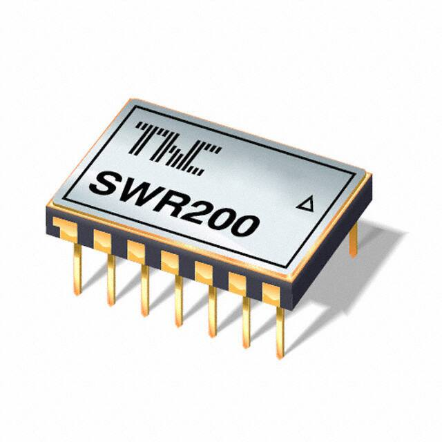


 工商网监
湘ICP备2023018690号
工商网监
湘ICP备2023018690号
