Features
• • • •
Overvoltage Monitoring Undervoltage Monitoring Cell Temperature Monitoring Self-diagnosis including – Comparator Functions – Communication Lines – Short and Open Measuring Lines Hot Plug-in Capable Less than 10 µA Stand-by Current Low Cell Imbalance Current (< 10 µA) Circuit Customization, e.g. for Over/Undervoltage Thresholds Possible for Adequate Volumes Cost-efficient Solution Due to Cost Optimized 30V CMOS Technology Daisy-chainable – Each IC Monitors 6 Battery Cells – 16 ICs (96 Cells) per String – No Limit on Number of Strings – Reliable Communication between Stacked ICs Due to Level Shifters with Current Sources Package SSO28
• • • • • •
Li-ion Battery Management Monitoring Emergency and Backup Circuit ATA6871 Preliminary
•
Applications
• Backup Battery-Cell Monitoring System for Li-ion Batteries • Emergency Indicator in Li-ion Batteries • Monitoring System in Li-ion Batteries
Benefits
• Highest Safety Level for Li-ion Battery Systems • Circuit Customization, e.g. Over and Undervoltage Thresholds, Possible for Large
Production Volumes
1. General Description
The ATA6871 is a battery cell monitoring circuit designed to act as an emergency, safety, or backup circuit in Li-ion battery systems for electrical and hybrid electrical vehicles (EV/HEV). It monitors overvoltage, undervoltage, and the cell temperature in Li-ion batteries without the need of a microcontroller. The circuit has an advanced self-test functionality, which checks the proper functionality of the monitoring comparators as well as the communication lines. It can be used as a monitoring circuit as well as an emergency indicator or as a backup system in Li-ion battery management systems. The ATA6871 can monitor four, five, or six battery cells. Up to 16 IC’s can be cascaded. If one or more battery cells exceed the over or undervoltage thresholds for longer than 2 seconds, or if the temperature input exceeds the temperature limit for more than 2 seconds, a digital output signal is set to high.
9123B–AUTO–07/09
�2. Block Diagram
Figure 2-1. Top-level Block Diagram
To ATA6871 above
VDDHV MBAT7 PD_N
MBAT6
Cell 6: Over-voltage Under-voltage Detection UV
6
Debouncing > 2 sec
OV 6 Input OR
Standby Control RC-OSC Self test
PD_N_OUT STATUS_IN
STATUS
3.3V Internal Voltage Regulator
MBAT2
VDD
BIASRES Cell 1: Over-voltage Under-voltage Detection UV Debouncing > 2 sec OV
6
6 Input OR
Internal Biasing
MBAT1 VDD
CHIPONE
Chip Configuration Debouncing > 2 sec
CHIPLAST CONF1 CONF0
TEMP_IN
Overtemperature comparator Test
OROUT_IN
4 Input OR
OROUT
NTC
VSSA
SCANMODE
CLK TEST_HV TEST_LV
ENUV
To ATA6871 below
2
ATA6871 [Preliminary]
9123B–AUTO–07/09
�ATA6871 [Preliminary]
3. Pin Configuration
Figure 3-1. Pinning SSO28
VDDHV MBAT7 MBAT6 MBAT5 MBAT4 MBAT3 MBAT2 MBAT1 TEST_HV 1 2 3 4 5 6 7 28 STATUS_IN 27 OROUT_IN 26 PD_N 25 PD_N_OUT 24 VDD 23 VDD 22 OROUT
ATA6871
8 9 21 STATUS 20 SCANMODE 19 CLK 18 ENUV 17 TEMP_IN 16 CONF0 15 CONF1
TEST_LV 10 VSSA 11 BIASRES 12 CHIPONE 13 CHIPLAST 14
Table 3-1.
Pin 1 2 3 4 5 6 7 8 9 10 11 12 13 14 15 16 17 18
Pin Description
Symbol VDDHV MBAT7 MBAT6 MBAT5 MBAT4 MBAT3 MBAT2 MBAT1 TEST_HV TEST_LV VSSA BIASRES CHIPONE CHIPLAST CONF1 CONF0 TEMP_IN ENUV Function Supply voltage Battery monitoring line Battery monitoring line Battery monitoring line Battery monitoring line Battery monitoring line Battery monitoring line Battery monitoring line Test-mode pin Test-mode pin Negative supply voltage Internal supply current adjustment Indicates circuit position in battery string (first, middle, last) Indicates circuit position in battery string (first, middle, last) Programs how many cells will be monitored (4, 5, or 6 cells operating) Programs how many cells will be monitored (4, 5, or 6 cells operating) Input for battery-cell temperature monitoring Enable/Disable under-voltage detection Keep pin open (output) Keep pin open (output) Remark
3
9123B–AUTO–07/09
�Table 3-1.
Pin 19 20 21 22 23 24 25 26 27 28
Pin Description
Symbol CLK SCANMODE STATUS OROUT VDD VDD PD_N_OUT PD_N OROUT_IN STATUS_IN Function Test-mode pin Test-mode pin Status output Output signal battery-cells in limits/out of limits Voltage regulator output Voltage regulator output Power down output Power down input Input for the OROUT signal of the upper ATA6871 circuit Input for the STATUS signal of the upper ATA6871 circuit Internally connected to pin 23 Remark Connected to VSSA Connected to VSSA
4
ATA6871 [Preliminary]
9123B–AUTO–07/09
�ATA6871 [Preliminary]
4. System Overview
The ATA6871 can be stacked in one string up to 16 times. Figure 4-1. Battery Management Architecture with one Battery String
ATA6871
ATA6871
ATA6871
ATA6871
2
Status/ Battery Cells OK, not OK
5
9123B–AUTO–07/09
�Figure 4-2.
Battery Management Architecture with Several Battery Strings
ATA6871
ATA6871 OPTO
ATA6871
2
ATA6871
2
Status/ Battery Cells OK, not OK
6
ATA6871 [Preliminary]
9123B–AUTO–07/09
�ATA6871 [Preliminary]
5. Absolute Maximum Ratings
Stresses beyond those listed under “Absolute Maximum Ratings” may cause permanent damage to the device. This is a stress rating only and functional operation of the device at these or any other conditions beyond those indicated in the operational sections of this specification is not implied. Exposure to absolute maximum rating conditions for extended periods may affect device reliability. Unless otherwise specified all voltages refer to pin VSSA. Logic Levels: 0 = VSSA, 1 = VDD. Parameters Ambient temperature Junction temperature Storage temperature Battery cell voltage VVDDHV - VVMBAT7max VMBAT1 Supply voltage Supply voltage (regulator is off) MBAT1 VDDHV VDD CHIPONE, CHIPLAST, CONF0, CONF1, SCANMODE, CLK, TEST_HV, TEST_LV, ENUV, OROUT BIASRES, TEMP_IN STATUS PD_N PD_N_OUT Pin Symbol TA TJ TS V(MBATi+1) - VMBATi VVDDHV - VVMBAT7 VMBAT1 VVDDHV VVDD VCHIPONE, VCHIPLAST, VCONF0, VCONF1, VSCANMODE, VCLK, VTEST_HV, VTEST_LV, VENUV, VOROUT VBIASRES, VTEMP_IN VSTATUS V PD_N V PD_N_OUT Min. –40 –40 –40 –0.3 –5.5 –0.3 –0.3 –0.3 Max. +85 +125 +150 +5.5 +0.3 +0.3 +30 +5.5 Unit °C °C °C V V V V V
Input voltage for logic I/O pins
–0.3
VDD + 0.3
V
Input voltage for analog low voltage input pins Logic output pin STATUS Input Output HBM ESD ANSI/ESD-STM5.1 JESD22-A114 AEC-Q100 (002) CDM ESD STM 5.3.1 CDM ESD STM 5.3.1 Latch Up according to AECQ100-004
–0.3 –0.3 –5.5
VDD + 0.3 +5.5 +0.3
V V V V V
Input voltage for digital high voltage input pins OROUT_IN, STATUS_IN VOROUT_IN, VSTATUS_IN VDDHV – 0.3 VDDHV + 0.3 VDDHV – 5.5 VDDHV + 0.3
ESD
±2
kV
500 VDDHV, CHIPLAST, CONF1, STATUS_IN ESD LATCH-UP 750 ±100
V V mA
6. Thermal Resistance
Parameters Maximum thermal resistance junction-ambient Symbol Rthja max Value 49 Unit K/W
7
9123B–AUTO–07/09
�7. Circuit Description and Electrical Characteristics
Unless otherwise specified, all parameters in this section are valid for a supply voltage range of 6.9V < V VDD HV < 3 0V and a battery cell voltage of V (MBATi+1) – V MBATi = 0 V to 5V, –40°C < TA < 85°C, all values refer to pin VSSA, unless otherwise specified.
7.1
Operating Modes
The ATA6871 has two operation modes: 1) Power-down Mode 2) ON Mode/Selfdiagnosis
7.1.1
Power-down Mode In Power-down Mode all blocks of the IC are switched off. The circuit can be switched from Power-down to ON Mode or back via the PD_N input. If the pin is connected to VDDHV, for example, via an external optocoupler the circuit is in ON Mode. If several ATA6871 are stacked, the power-down signal must be only provided for the IC on the top level of the stack. The next lower IC is getting this information from the PD_N_OUT output of it's upper IC. The PD_N_OUT pin must be connected either to the PD_N pin of the next lower ATA6871 or to VSSA.
8
ATA6871 [Preliminary]
9123B–AUTO–07/09
�ATA6871 [Preliminary]
Figure 7-1. Power-down
VDDHV PD_N MBAT7
MBAT6
OV Cell 1: Over-voltage Under-voltage Detection UV
Debouncing > 2 sec
Standby Control RC-OSC Self test
PD_N_OUT
6
6 Input OR
ATA6871
MBAT2
3.3V Internal Voltage Regulator
VDD
MBAT1
OV Cell 6: Over-voltage Under-voltage Detection UV
Debouncing > 2 sec
6
6 Input OR
Internal Biasing
Chip Configuration Debouncing > 2 sec
CHIPLAST CHIPONE
Overtemperature comparator
TEMP_IN
4 Input OR
Test
VSSA
ENUV
VDDHV MBAT7 PD_N
Debouncing > 2 sec
MBAT6
Cell 1: Over-voltage Under-voltage Detection UV
OV
6
Standby Control RC-OSC Self test
PD_N_OUT
6 Input OR
ATA6871
MBAT2
3.3V Internal Voltage Regulator
VDD
MBAT1
OV Cell 6: Over-voltage Under-voltage Detection UV
Debouncing > 2 sec
6
6 Input OR
Internal Biasing
Chip Configuration Debouncing > 2 sec
CHIPLAST CHIPONE
Overtemperature comparator
TEMP_IN
4 Input OR
Test
VSSA
ENUV
9
9123B–AUTO–07/09
�Table 7-1.
Electrical Characteristics
Test Conditions Pin Symbol Min. Typ. Max. Unit Type*
No. Parameters Maximum allowed input current in Power-down 1.1 Mode (e.g., leakage current of an optocoupler) 1.2 Input current in ON Mode Current consumption in 1.3 Power-down Mode IVDDHV + IMBATi_max(1)
PD_N
IPD_N IPD_N 2.5
50
µA
A
PD_N VMBAT(i+1) – VMBAT(i) = 3.7V
5 10
mA µA
A A
Imbalance from battery cell VMBAT(i+1) – 1.4 to battery cell in VMBAT(i) = 3.7V Power-down Mode 1.5 Maximum input voltage (Power-down Mode) IPD_N = 0 to 50 µA PD_N VVDDHV – VPD_N tVDDON
10
µA
A
5
V
A
Propagation delay time 1.6 from Power-down Mode to CVDD = 10 nF ON Mode Propagation delay time 1.7 from ON Mode to Power-down Mode Note: CVDD = 10 nF
VDD
1
ms
A
VDD
tVDDOFF
11
ms
A
*) Type means: A = 100% tested, B = 100% correlation tested, C = Characterized on samples, D = Design parameter 1. Largest input current of the inputs MBAT1 to MBAT7
7.1.2
ON Mode/Selfdiagnosis When the PD_N-signal goes from low to high, the self diagnosis of the ATA6871 starts. During this self diagnosis the following tests are performed: • Test if over/undervoltage or overtemperature comparators are able to switch or if they stuck to 0 or 1 • Test if pins OROUT_IN, OROUT in stacked ICs are able to switch or if they stuck to 0 or 1 and if the connection to next ATA6871 is available or not • Test if pins STATUS_IN, STATUS are able to switch or if they stuck to 0 or 1 and if the connection to next ATA6871/MCU is available or not • Detect open or shorted input pins MBAT1 to MBAT7 • Detect wrong setting of CONF0, CONF1 (e.g. 4 cell configuration programmed, 6 cells used) If self diagnosis fails, the STATUS of the lowest ATA6871 is constant low. If the self diagnosis succeeds, the STATUS of the lowest ATA6871 is toggling.
10
ATA6871 [Preliminary]
9123B–AUTO–07/09
�ATA6871 [Preliminary]
The circuit will suppress failures detected during the self test and provide only results from good tested comparators connections to pin OROUT. This enables the system to monitor the rest of the battery cells if one connection/comparator fails. If, for example, the connection of the OROUT signal between two ATA6871s is open, the OROUT_IN signal of the lower ATA6871 will be ignored, but all the cells of this ATA6871 and ICs below will be observed in the normal way. If the battery cell voltage exceeds 4.9V or is below 1.5V during the self-diagnosis, the affected comparator will be detected as defect, and the output of the affected comparator will be also suppressed until the next self diagnosis. If, after the self test has passed, one of the comparator in the stack detects under or overtemperature at a battery cell, the output OROUT switches from low to high. The battery cell undervoltage detection can be disabled with the digital input ENUV.
Table 7-2.
No. 2.1 2.2 2.3
Electrical Characteristics
Test Conditions No external load Self diagnosis ongoing or failed Self diagnosis passed successful i = number of stacked ICs Pin VDDHV VDDHV MBAT(i) Symbol VVDDHV IVDDHV IMBAT(i) Constant low 15 tselfdiag 2+ 0.85 × i Toggle frequency 50 8+ 2.2 × i Hz ms Min. 6.9 Typ. Max. 30 6 5 Unit V mA µA Type* A A A A A B
Parameters Supply voltage Current consumption Input current
2.4
Digital output signal
STATUS
VSTATUS
2.5
Self diagnosis time
*) Type means: A = 100% tested, B = 100% correlation tested, C = Characterized on samples, D = Design parameter
7.2
Battery Cell Over and Undervoltage Detection
If, after the self diagnosis of the chip has passed, one of the monitored battery cell voltages V(MBATi+1) - VMBATi is above the overvoltage threshold or below the undervoltage threshold for t > tDebounce, the OROUT output goes high. The battery cell undervoltage detection can be disabled with the digital input ENUV.
Table 7-3.
PIN ENUV
Truth Table:
Symbol Value 0 1 Function Undervoltage detection disabled Undervoltage detection enabled
VENUV
11
9123B–AUTO–07/09
�Table 7-4.
No. 3.1 3.2 3.3 3.4 3.5 3.6 3.7
Electrical Characteristics
Test Conditions Pin MBAT(i) MBAT(i) MBAT(i) MBAT(i) MBAT(i) MBAT(i) Symbol V(MBAT(i+1)) – VMBAT(i) V(MBAT(i+1)) – VMBAT(i) ΔV(MBAT(i+1)) – VMBAT(i) V(MBAT(i+1)) – VMBAT(i) V(MBAT(i+1)) – VMBAT(i) ΔV(MBAT(i+1)) – VMBAT(i) tDebounce Min. 4.3 4.2 70 1.7 1.8 70 1 3 1.8 1.9 1.9 2.0 Typ. 4.45 4.35 Max. 4.6 4.5 Unit V V mV V V mV s Type* A A A A A A A
Parameters Overvoltage detection on threshold Overvoltage detection off threshold Overvoltage detection hysteresis Undervoltage detection on threshold Undervoltage detection off threshold Undervoltage detection hysteresis Debouncing time
*) Type means: A = 100% tested, B = 100% correlation tested, C = Characterized on samples, D = Design parameter
7.3
Battery Cell Overtemperature Detection
If the voltage at the input TEMP_IN is less than the half of VDD threshold for t > tDebounce, the OROUT output goes high. To disable this function, connect TEMP_IN to VDD. If the input is open (high impedance), an internal current will force the comparator to the overtemperature state and OROUT will switch to high. Figure 7-2. Overtemperature Detection
VDD
Rref TEMP_IN Overtemp
NTC
ITEMP_IN
VDD/2
VSSA
12
ATA6871 [Preliminary]
9123B–AUTO–07/09
�ATA6871 [Preliminary]
Table 7-5. Electrical Characteristics
Test Conditions Pin TEMP_IN TEMP_IN TEMP_IN Symbol VTEMP_IN VTEMP_IN ΔVTEMP_IN RDivider = RNTC + RRref VTEMP_IN=1.65V TEMP_IN ITEMP_IN tDebounce Min. VDD/2 – 100 mV VDD/2 – 50 mV 30 3 0.4 1 1000 0.6 3 Typ. VDD/2 VDD/2 + 50 mV Max. VDD/2 + 100 mV VDD/2 + 150 mV Unit V V mV kΩ µA s Type* A A A D A A
No. Parameters 4.1 4.2 4.3 4.4 4.5 4.6 Overtemperature detection on threshold Overtemperature detection off threshold Overtemperature detection hysteresis Resistor Divider Input Current Debouncing Time
*) Type means: A = 100% tested, B = 100% correlation tested, C = Characterized on samples, D = Design parameter
7.4
7.4.1
ATA6871 Configuration
Device Position The ATA6871 can be cascaded up to 16 times in one string. The input pins CHIPONE and CHIPLAST define the first and the last IC in a string.
Table 7-6.
CHIPONE 0 0 1 1
Device Position
CHIPLAST 0 1 0 1 Configuration ICs between the first and the last IC (up to 14 ICs) Last cascaded chip, connected to power down optocoupler First chip in a string (master) First and last chip: (if only one IC is used per string)
7.4.2
Number of Cells Configuration The ATA6871 can work with either four, five, or six cells. This can be programmed with the input pins CONF0 and CONF1. When used with 5 cells, the inputs MBAT5 and 6 must be connected together, when used with 4 cells the inputs MBAT4, MBAT5 and MBAT6 must be connected together (see also Figure 7-3 to Figure 7-5).
Table 7-7.
CONF1 0
Cells Configuration
CONF0 0 Configuration 4 cells configuration Notes Over/undervoltage comparators between MBAT4,5 and MBAT6 are disabled Over/undervoltage comparator between MBAT5 and MBAT6 is disabled
0 1 1
1 0 1
5 cells configuration Do not use, reserved for test purposes 6 cells configuration
13
9123B–AUTO–07/09
�Figure 7-3.
6 Cells Operation
MBAT7
MBAT6
MBAT5
VDDHV VDD
MBAT4
ATA6871
MBAT3
MBAT2
MBAT1
VSSA
CONF1
CONF0
Figure 7-4.
5 Cells Operation
MBAT7
MBAT6
MBAT5
VDDHV VDD
MBAT4
ATA6871
MBAT3
MBAT2
MBAT1
VSSA
CONF1
CONF0
14
ATA6871 [Preliminary]
9123B–AUTO–07/09
�ATA6871 [Preliminary]
Figure 7-5. 4 Cells Operation
MBAT7
MBAT6
MBAT5
VDDHV VDD
MBAT4
ATA6871
MBAT3
MBAT2
MBAT1
VSSA
CONF1
CONF0
15
9123B–AUTO–07/09
�7.5
7.5.1
Supplies
Voltage Regulator The circuit includes a linear 3.3V voltage regulator, which supplies internal blocks as well as external components, e.g., the resistor divider for the over-temperature measurement. The regulator is supplied out of VDDHV. A load capacitor of 10 nF has to be used for stabilization purposes.
Table 7-8.
No. 5.1 5.2 5.3
Electrical Characteristics
Test Conditions Pin VDD VDD VDD Symbol VVDD IVDD Cload Min. 3.1 –5 8 10 12 Typ. 3.3 Max. 3.5 Unit V mA nF Type* A A D
Parameters Output voltage Maximum output current for external components Load capacitor
*) Type means: A = 100% tested, B = 100% correlation tested, C = Characterized on samples, D = Design parameter
7.5.2
Central Biasing This block generates a precise bias current to supply internal blocks of the IC. External load cannot be connected to this pin.
Table 7-9.
No. 6.1 6.2 6.3 6.4
Electrical Characteristics
Test Conditions Pin BIASRES Symbol VBIASRES RRefbias ΔRRefbias BIASRES CExternal –1 Min. Typ. 1.2 121 +1 50 Max. Unit V kΩ % pF Type* A D D D
Parameters Biasing voltage External resistor Tolerance Maximum external parasitic capacitor
*) Type means: A = 100% tested, B = 100% correlation tested, C = Characterized on samples, D = Design parameter
16
ATA6871 [Preliminary]
9123B–AUTO–07/09
�ATA6871 [Preliminary]
Figure 7-6. Internal Bias Current Generation
IBIAS
Bandgap 1.2V BIASRES RREFBIAS 121 kΩ VSSA
17
9123B–AUTO–07/09
�7.6
7.6.1
Digital Inputs and Outputs
Digital Output Characteristics If the ATA6871 is configured as first IC (master) in a string (CHIPONE = 1, CHIPLAST = 0 or 1), the output OROUT acts as a push-pull output, the output STATUS as an open drain output. If the ATA6871 is configured to be a stacked IC (CHIPONE = 0, CHIPLAST = 0 or 1), the output signals STATUS and OROUT coming from the upper IC need to be transferred to the STATUS and OROUT output of the master in the string via the STATUS_IN and OROUT_IN inputs. In this case the OROUT and STATUS outputs act as level shifters based on current sources.
Table 7-10.
No. 7.1 7.2 7.3 7.4
Digital Output Characteristics (OROUT, STATUS)
Test Conditions Iout = –5 mA CHIPONE = 1 Iout = +5 mA CHIPONE = 1 Vout = –0.3V to +0.3V, CHIPONE = 0 Vout = –0.3V to +0.3V, CHIPONE = 0 Pin OROUT OROUT, STATUS OROUT, STATUS OROUT, STATUS Symbol VOROUT, VOROUT, VSTATUS IOROUT, ISTATUS IOROUT, ISTATUS –13 –65 Min. 0.8 × VDD 0.2 × VDD –8 –44 Typ. Max. Unit V V µA µA Type* A A A A
Parameters High-level output voltage Low-level output voltage Low-level output current High-level output current
*) Type means: A = 100% tested, B = 100% correlation tested, C = Characterized on samples, D = Design parameter
7.6.2
Digital Input Characteristics Digital Input Characteristics (OROUT_IN, STATUS_IN)
Test Conditions (VDDHV + 1.4V) ±300 mV (VDDHV + 1.4V) ±300 mV Pin OROUT_IN, STATUS_IN OROUT_IN, STATUS_IN Symbol IOROUT_IN, ISTATUS_IN IOROUT_IN, ISTATUS_IN Min. 15 42 Typ. Max. Unit µA µA Type* A A
Table 7-11.
No. 8.1 8.2
Parameters Low-level input current High-level input current
*) Type means: A = 100% tested, B = 100% correlation tested, C = Characterized on samples, D = Design parameter
18
ATA6871 [Preliminary]
9123B–AUTO–07/09
�ATA6871 [Preliminary]
Table 7-12.
No.
Digital Input Characteristics PINs CHIPONE, CHIPLAST, CONF0, CONF1, ENUV
Test Conditions Pin CHIPONE, CHIPLAST, CONF0, CONF1, ENUV CHIPONE, CHIPLAST, CONF0, CONF1, ENUV CHIPONE, CHIPLAST, CONF0, CONF1, ENUV CHIPONE, CHIPLAST, CONF0, CONF1, ENUV Symbol VCHIPONE, VCHIPLAST, VCONF0, VCONF1, VENUV VCHIPONE, VCHIPLAST, VCONF0, VCONF1, VENUV VCHIPONE, VCHIPLAST, VCONF0, VCONF1, VENUV VCHIPONE, VCHIPLAST, VCONF0, VCONF1, VENUV 0.05 × VDD Min. 0.7 × VDD Typ. Max. Unit Type*
Parameters
9.1
High-level input voltage
VDD
V
A
9.2
Low-level input voltage
0.3 × VDD
V
A
9.3
Hysteresis
V
C
9.4
Input current
1
µA
A
*) Type means: A = 100% tested, B = 100% correlation tested, C = Characterized on samples, D = Design parameter
7.6.3
Test-mode Pins The test-mode pins TEST_HV, TEST_LV (outputs) have to be kept open in the application. The test-mode pins CLK, SCANMODE (inputs) have to be connected to VSSA. These inputs have an internal pull-down resistor.
Table 7-13.
No. 10.1
Digital Input Characteristics PINs SCANMODE, CLK
Test Conditions Pin SCANMODE, CLK Symbol RSCANMODE, RCLK Min. 50 Typ. Max. 200 Unit kΩ Type* A
Parameters Pull-down resistor
*) Type means: A = 100% tested, B = 100% correlation tested, C = Characterized on samples, D = Design parameter
19
9123B–AUTO–07/09
�8. Application
Figure 8-1 shows an application with 3 stacked ATA6871s. The ATA6871 on the highest potential, is configured to monitor only four instead of six battery cells. Figure 8-1. Typical Application
50Ω Power Down 1 kΩ 100 nF
MBAT7
CHIPLAST CHIPONE SCANMODE
1 kΩ
MBAT6
CLK BIASRES
121 kΩ
1.5 kΩ
MBAT5
VDDHV VDD
100 nF 10 nF
MBAT4
1 kΩ 100 nF
ATA6871
MBAT3
OROUT_IN OROUT PD_N
1 kΩ
100 nF
MBAT2
100 nF
PD_N_OUT STATUS_IN
1 kΩ
MBAT1 TEMP_IN VSSA CONF1 CONF0
STATUS ENUV
RREF
NTC 50Ω
1 kΩ 100 nF
MBAT7
CHIPLAST CHIPONE SCANMODE
1 kΩ
MBAT6
100 nF
CLK BIASRES
121 kΩ
1 kΩ
MBAT5
100 nF
VDDHV VDD
100 nF 10 nF
1 kΩ
MBAT4
100 nF
ATA6871
MBAT3
1 kΩ
OROUT_IN OROUT PD_N
1 kΩ
100 nF
MBAT2
100 nF
PD_N_OUT STATUS_IN
1 kΩ
MBAT1 TEMP_IN VSSA CONF1 CONF0
STATUS ENUV
RREF
NTC 50Ω
1 kΩ 100 nF
MBAT7
CHIPLAST CHIPONE SCANMODE
1 kΩ
MBAT6
100 nF
CLK BIASRES
121 kΩ
1 kΩ
MBAT5
100 nF
VDDHV VDD
100 nF 10 nF
1 kΩ
MBAT4
100 nF
ATA6871
MBAT3
ROROUT 51 kΩ To Emergency Relais
1 kΩ
OROUT_IN OROUT PD_N
1 kΩ
100 nF
MBAT2
100 nF
PD_N_OUT STATUS_IN
51 kΩ
Microcontroller Supploy
1 kΩ
MBAT1 TEMP_IN VSSA CONF1 CONF0
STATUS ENUV
Microcontroller
RREF
NTC 50Ω
Note:
ROROUT can be used to check if the connection between the lowest ATA6871 and the emerging Relays is available.
20
ATA6871 [Preliminary]
9123B–AUTO–07/09
�ATA6871 [Preliminary]
9. Ordering Information
Extended Type Number ATA6871-TLPW ATA6871-TLQW Package SSO28 SSO28 MOQ 1,000 pieces 4,000 pieces
10. Package Information
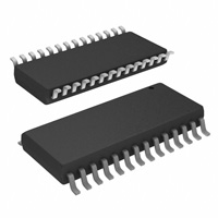
The IC is packaged in a SSO28 package — green (lead-free/RoHS) package.
5.4±0.2 9.35-0.25 4.4±0.1
0.05+0.1
1.3±0.05
0.25±0.05 0.65±0.05 8.45±0.05
6.45±0.15
28
15
Package: SSO28 Dimensions in mm
technical drawings according to DIN specifications
1 Drawing-No.: 6.543-5056.03-4 Issue: 1; 10.03.04
14
0.15±0.05
21
9123B–AUTO–07/09
�11. Revision History
Please note that the following page numbers referred to in this section refer to the specific revision mentioned, not to this document. Revision No. History • Table 5 “Absolute Maximum Ratings” on page 7 changed • Table 7-1 “Electrical Characteristics” on page 10 changed • Heading “ON-Mode/Selfdiagnosis” on page 10 changed • Table 7-4 “Electrical Characteristics” on page 12 changed • Table 7-8 “Electrical Characteristics” on page 16 changed • Table 7-10 “Digital Output Characteristics (OROUT, STATUS)” on page 19 changed • Table 7-11 “Digital Input Characteristics (OROUT_IN, STATUS_IN)” on page 19 changed • Table 7-12 “Digital Input Characteristics PINs CHIPONE, CHIPLAST, CONF0, CONF1, ENUV” on page 19 changed
9123B-AUTO-07/09
22
ATA6871 [Preliminary]
9123B–AUTO–07/09
�Headquarters
Atmel Corporation 2325 Orchard Parkway San Jose, CA 95131 USA Tel: 1(408) 441-0311 Fax: 1(408) 487-2600
International
Atmel Asia Unit 1-5 & 16, 19/F BEA Tower, Millennium City 5 418 Kwun Tong Road Kwun Tong, Kowloon Hong Kong Tel: (852) 2245-6100 Fax: (852) 2722-1369 Atmel Europe Le Krebs 8, Rue Jean-Pierre Timbaud BP 309 78054 Saint-Quentin-en-Yvelines Cedex France Tel: (33) 1-30-60-70-00 Fax: (33) 1-30-60-71-11 Atmel Japan 9F, Tonetsu Shinkawa Bldg. 1-24-8 Shinkawa Chuo-ku, Tokyo 104-0033 Japan Tel: (81) 3-3523-3551 Fax: (81) 3-3523-7581
Product Contact
Web Site www.atmel.com Technical Support auto_control@atmel.com Sales Contact www.atmel.com/contacts
Literature Requests www.atmel.com/literature
Disclaimer: T he information in this document is provided in connection with Atmel products. No license, express or implied, by estoppel or otherwise, to any intellectual property right is granted by this document or in connection with the sale of Atmel products. EXCEPT AS SET FORTH IN ATMEL’S TERMS AND CONDITIONS OF SALE LOCATED ON ATMEL’S WEB SITE, ATMEL ASSUMES NO LIABILITY WHATSOEVER AND DISCLAIMS ANY EXPRESS, IMPLIED OR STATUTORY WARRANTY RELATING TO ITS PRODUCTS INCLUDING, BUT NOT LIMITED TO, THE IMPLIED WARRANTY OF MERCHANTABILITY, FITNESS FOR A PARTICULAR PURPOSE, OR NON-INFRINGEMENT. IN NO EVENT SHALL ATMEL BE LIABLE FOR ANY DIRECT, INDIRECT, CONSEQUENTIAL, PUNITIVE, SPECIAL OR INCIDENTAL DAMAGES (INCLUDING, WITHOUT LIMITATION, DAMAGES FOR LOSS OF PROFITS, BUSINESS INTERRUPTION, OR LOSS OF INFORMATION) ARISING OUT OF THE USE OR INABILITY TO USE THIS DOCUMENT, EVEN IF ATMEL HAS BEEN ADVISED OF THE POSSIBILITY OF SUCH DAMAGES. Atmel makes no representations or warranties with respect to the accuracy or completeness of the contents of this document and reserves the right to make changes to specifications and product descriptions at any time without notice. Atmel does not make any commitment to update the information contained herein. Unless specifically provided otherwise, Atmel products are not suitable for, and shall not be used in, automotive applications. Atmel’s products are not intended, authorized, or warranted for use as components in applications intended to support or sustain life.
© 2009 Atmel Corporation. All rights reserved. A tmel ®, Atmel logo and combinations thereof, and others are registered trademarks or trademarks of Atmel Corporation or its subsidiaries. Other terms and product names may be trademarks of others.
9123B–AUTO–07/09
�


 工商网监
湘ICP备2023018690号
工商网监
湘ICP备2023018690号
