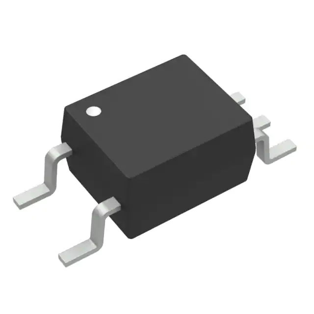
ACPL-M46T
Automotive Intelligent Power Module
with R2Coupler™ Isolation and Small Outline, 5 Lead Package
Data Sheet
Lead (Pb) Free
RoHS 6 fully
compliant
RoHS 6 fully compliant options available;
-xxxE denotes a lead-free product
Description
Features
The ACPL-M46T consists of a AlGaAs optically coupled
to an integrated high gain photo detector. Minimized
propagation delay difference between devices make
these optocouplers excellent solutions for improving automotive inverter efficiency through reduced switching
dead time.
Performance specified for common IPM applications
over automotive temperature range: -40°C to 125°C
Specification and performance plots are given for typical
IPM applications.
Very high Common Mode Rejection (CMR):
15 kV/μs at VCM = 1500 V
Avago R2Coupler isolation products provide the reinforced insulation and reliability needed for critical in automotive and high temperature industrial applications.
Fast maximum propagation delays
- tPHL & tPLH = 550 ns
Minimized Pulse Width Distortion (PWD = 370 ns)
CTR > 44% at IF = 10 mA
Qualified to AEC-Q100 Test Guidelines
Safety approval
- UL recognized per UL1577 (file no. E55361)
4000 Vrms for 1 minute
Schematic Diagram
- IEC/EN/DIN EN 60747-5-2 Approved
ANODE
1
CATHODE 3
SHIELD
6
VCC
5
VOUT
4
GND
Truth Table
- CSA Approved
LED
VO
Applications
ON
L
OFF
H
Automotive IPM isolation for battery management
system and motor control
The connection of a 0.1 μF bypass capacitor between pins 4 and 6 is
recommended.
Isolated IGBT/MOSFET gate drive
AC and brushless dc motor drives
Industrial inverters for power supplies and motor
controls
CAUTION: It is advised that normal static precautions be taken in handling and assembly
of this component to prevent damage and/or degradation which may be induced by ESD.
�Ordering Information
Option
Part Number
(RoHS) Compliant
Package
-000E
SO-5
ACPL-M46T
Surface
Mount
Tape &
Reel
IEC/EN/DIN EN
60747-5-2
Quantity
X
100 per tube
-060E
X
X
-500E
X
X
-560E
X
X
100 per tube
1500 per reel
X
1500 per reel
To order, choose a part number from the part number column and combine with the desired option from the option
column to form an order entry.
Example 1:
ACPL-M46T-500E to order product of SO-5 Surface Mount package in Tape and Reel packaging with RoHS
compliant.
Example 2:
ACPL-M46T-000E to order product of SO-5 Surface Mount package in tube packaging with RoHS compliant.
Option datasheets are available. Contact your Avago sales representative or authorized distributor for information.
Package Outline Drawing
ACPL-M46T-000E Small Outline SO-5 Package (JEDEC MO-155)
Land Pattern Recommendation
4.4
(0.17)
M46T
YWW
4.4 ± 0.1
(0.173 ± 0.004)
7.0 ± 0.2
(0.276 ± 0.008)
EE
2.5
(0.10)
Extended
Datecode
for lot tracking
2.0
(0.080)
0.64
(0.025)
8.27
(0.325)
0.4 ± 0.05
(0.016 ± 0.002)
3.6 ± 0.1*
(0.142 ± 0.004)
2.5 ± 0.1
(0.098 ± 0.004)
1.3
(0.05)
DIMENSION IN MILLIMETERS (INCHES)
0.102 ± 0.102
(0.004 ± 0.004)
0.20 ± 0.025
(0.008 ± 0.001)
7° MAX.
1.27 BSC
(0.050)
DIMENSIONS IN MILLIMETERS (INCHES)
* MAXIMUM MOLD FLASH ON EACH SIDE IS 0.15 mm (0.006)
NOTE: FLOATING LEAD PROTRUSION IS 0.15 mm (6 mils) MAX.
2
0.71 MIN
(0.028)
MAX. LEAD COPLANARITY
= 0.102 (0.004)
�Recommended Pb-Free IR Profile
Recommended reflow condition as per JEDEC Standard, J-STD-020 (latest revision).
Note: Non-halide flux should be used
Regulatory Information
The ACPL-M46T is approved by the following organizations:
UL
IEC/EN/DIN EN 60747-5-2
Approved under UL 1577, component recognition program up to VISO = 4000 VRMS
Approved under:
IEC 60747-5-2:2007
EN 60747-5-2:2001 + A1
DIN EN 60747-5-2 (VDE 0884 Teil 2)
CSA
Approved under CSA Component Acceptance Notice
#5.
IEC/EN/DIN EN 60747-5-2 Insulation Characteristics*
Description
Symbol
Installation classification per DIN VDE 0110/1.89, Table 1
for rated mains voltage ≤ 150 Vrms
for rated mains voltage ≤ 300 Vrms
for rated mains voltage ≤ 600 Vrms
Characteristic
Unit
I – IV
I – III
I – II
Climatic Classification
55/125/21
Pollution Degree (DIN VDE 0110/1.89)
2
Maximum Working Insulation Voltage
VIORM
567
Vpeak
Input to Output Test Voltage, Method b*
VIORM x 1.875=VPR, 100% Production Test with tm=1 sec, Partial discharge < 5 pC
VPR
1063
Vpeak
Input to Output Test Voltage, Method a*
VIORM x 1.6=VPR, Type and Sample Test, tm=10 sec, Partial discharge < 5 pC
VPR
907
Vpeak
Highest Allowable Overvoltage (Transient Overvoltage tini = 60 sec)
VIOTM
6000
Vpeak
Safety-limiting values – maximum values allowed in the event of a failure.
Case Temperature
Input Current
Output Power
TS
IS, INPUT
PS, OUTPUT
175
230
600
°C
mA
mW
Insulation Resistance at TS, VIO = 500 V
RS
>109
W
*
3
Refer to the optocoupler section of the Isolation and Control Components Designer’s Catalog, under Product Safety Regulations section, (IEC/
EN/DIN EN 60747-5-2) for a detailed description of Method a and Method b partial discharge test profiles.
�Insulation Related Specifications
Parameter
Symbol
Value
Units
Conditions
Minimum External Air Gap
(Clearance)
L(101)
≥5
mm
Measured from input terminals to output
terminals, shortest distance through air.
Minimum External Tracking
(Creepage)
L(102)
≥5
mm
Measured from input terminals to output
terminals, shortest distance path along body.
0.08
mm
Through insulation distance conductor to
conductor, usually the straight line distance
thickness between the emitter and detector.
200
Volts
DIN IEC 112/VDE 0303 Part 1
Minimum Internal Plastic Gap
(Internal Clearance)
Tracking Resistance
(ComparativeTracking Index)
CTI
Isolation Group
IIIa
Material Group (DIN VDE 0110)
Absolute Maximum Ratings
Parameter
Symbol
Min.
Max.
Units
Storage Temperature
TS
-55
150
°C
Operating Temperature
TA
-40
125
°C
Average Input Current
IF(avg)
20
mA
Peak Input Current
(50% duty cycle, 11.0 V).
8. Common mode transient immunity in a Logic Low level is the maximum tolerable dVCM/dt of the common mode pulse, VCM, to assure that the
output will remain in a Logic Low state (i.e., VO < 1.0 V).
9. Pulse Width Distortion (PWD) is defined as |tPHL - tPLH| for any given device.
6
�LED Drive Circuit Considerations For Ultra High CMR
Performance
Without a detector shield, the dominant cause of optocoupler CMR failure is capacitive coupling from the
input side of the optocoupler, through the package, to
the detector IC as shown in Figure 14. The ACPL-M46T
improves CMR performance by using a detector IC with
an optically transparent Faraday shield, which diverts
the capacitively coupled current away from the sensitive
IC circuitry. However, this shield does not eliminate the
capacitive coupling between the LED and the optocoupler output pin and output ground as shown in Figure
15. This capacitive coupling causes perturbations in the
LED current during common mode transients and becomes the major source of CMR failures for a shielded
optocoupler. The main design objective of a high CMR
LED drive circuit becomes keeping the LED in the proper
state (on or off ) during common mode transients. For example, the recommended application circuit (Figure 13),
can achieve 15 kV/μs CMR while minimizing component
complexity. Note that a CMOS gate is recommended in
Figure 13 to keep the LED off when the gate is in the high
state.
Another cause of CMR failure for a shielded optocoupler
is direct coupling to the optocoupler output pins through
CLEDO1 in Figure 15. Many factors influence the effect and
magnitude of the direct coupling including: the position
of the LED current setting resistor and the value of the
capacitor at the optocoupler output (CL).
Techniques to keep the LED in the proper state and minimize the effect of the direct coupling are discussed in the
next two sections.
CMR with the LED on (CMRL)
A high CMR LED drive circuit must keep the LED on during common mode transients. This is achieved by overdriving the LED current beyond the input threshold so
that it is not pulled below the threshold during a transient. The recommended minimum LED current of 10 mA
provides adequate margin over the maximum ITH of 4.0
mA (see Figure 2) to achieve 15 kV/μs CMR.
The placement of the LED current setting resistor effects
the ability of the drive circuit to keep the LED on during transients and interacts with the direct coupling to
the optocoupler output. For example, the LED resistor in
Figure 16 is connected to the anode. Figure 17 shows the
AC equivalent circuit for Figure 16 during common mode
transients. During a +dVCM/dt in Figure 17, the current
available at the LED anode (Itotal) is limited by the series
resistor. The LED current (IF) is reduced from its DC value
by an amount equal to the current that flows through
CLEDP and CLEDO1. The situation is made worse because the
7
current through CLEDO1 has the effect of trying to pull the
output high (toward a CMR failure) at the same time the
LED current is being reduced. For this reason, the recommended LED drive circuit (Figure 13) places the current
setting resistor in series with the LED cathode. Figure 18
is the AC equivalent circuit for Figure 13 during common
mode transients. In this case, the LED current is not reduced during a +dVCM/dt transient because the current
flowing through the package capacitance is supplied by
the power supply. During a dVCM/dt transient, however,
the LED current is reduced by the amount of current
flowing through CLEDN. But, better CMR performance
is achieved since the current flowing in CLEDO1 during a
negative transient acts to keep the output low.
CMR with the LED Off (CMRH)
A high CMR LED drive circuit must keep the LED off (VF
≤ VF(OFF)) during common mode transients. For example,
during a +dVCM/dt transient in Figure 18, the current
flowing through CLEDN is supplied by the parallel combination of the LED and series resistor. As long as the voltage developed across the resistor is less than VF(OFF) the
LED will remain off and no common mode failure will occur. Even if the LED momentarily turns on, the 100 pF capacitor from pins 5-4 will keep the output from dipping
below the threshold. The recommended LED drive circuit (Figure 13) provides about 10 V of margin between
the lowest optocoupler output voltage and a 3 V IPM
threshold during a 15kV/μs transient with VCM = 1500 V.
Additional margin can be obtained by adding a diode
in parallel with the resistor, as shown by the dashed line
connection in Figure 18, to clamp the voltage across the
LED below VF(OFF).
Since the open collector drive circuit, shown in Figure 19,
cannot keep the LED off during a +dVCM/dt transient, it is
not desirable for applications requiring ultra high CMRH
performance. Figure 20 is the AC equivalent circuit for
Figure 19 during common mode transients. Essentially
all the current flowing through CLEDN during a +dVCM/
dt transient must be supplied by the LED. CMRH failures
can occur at dv/dt rates where the current through the
LED and CLEDN exceeds the input threshold. Figure 21 is
an alternative drive circuit which does achieve ultra high
CMR performance by shunting the LED in the off state.
�IPM Dead Time and Propagation Delay Specifications
The ACPL-M46T includes a Propagation Delay Difference
specification intended to help designers minimize “dead
time” in their power inverter designs. Dead time is the
time period during which both the high and low side
power transistors (Q1 and Q2 in Figure 22) are off. Any
overlap in Q1 and Q2 conduction will result in large currents flowing through the power devices between the
high and low voltage motor rails.
To minimize dead time the designer must consider the
propagation delay characteristics of the optocoupler as
well as the characteristics of the IPM IGBT gate drive circuit. Considering only the delay characteristics of the optocoupler (the characteristics of the IPM IGBT gate drive
circuit can be analyzed in the same way) it is important
to know the minimum and maximum turn-on (tPHL) and
turn-off (tPLH) propagation delay specifications, preferably over the desired operating temperature range.
The limiting case of zero dead time occurs when the input to Q1 turns off at the same time that the input to Q2
turns on. This case determines the minimum delay between LED1 turn-off and LED turn-on, which is related
to the worst case optocoupler propagation delay waveforms, as shown in Figure 23. A minimum dead time of
zero is achieved in Figure 23 when the signal to turn on
LED is delayed by (tPLH max - tPHL min) from the LED1 turn
off. Note that the propagation delays used to calculate
PDD are taken at equal temperatures since the optocouplers under consideration are typically mounted in close
proximity to each other. (Specifically, tPLH max and tPHL min
in the previous equation are not the same as the tPLH max
and tPHL min, over the full operating temperature range,
specified in the data sheet.) This delay is the maximum
value for the propagation delay difference specification
which is specified at 370 ns for the ACPL-M46T over an
operating temperature range of -40°C to 125°C.
Delaying the LED signal by the maximum propagation
delay difference ensures that the minimum dead time is
zero, but it does not tell a designer what the maximum
dead time will be. The maximum dead time occurs in
the highly unlikely case where one optocoupler with
the fastest tPLH and another with the slowest tPHL are in
the same inverter leg. The maximum dead time in this
case becomes the sum of the spread in the tPLH and tPHL
propagation delays as shown in Figure 24. The maximum
dead time is also equivalent to the difference between
the maximum and minimum propagation delay difference specifications. The maximum dead time (due to the
optocouplers) for the ACPL-M46T is 520 ns (= 370 ns (-150 ns)) over an operating temperature range of -40°C
to 125°C.
1.05
25°C
10
125°C
8
-40°C
6
VO =0.6V
4
2
0
0
5
10
IF - FORWARD CURRENT - mA
Figure 2. Typical Transfer Characteristics.
8
15
20
NORMALIZED OUTPUT CURRENT
IO - OUTPUT CURRENT - mA
12
1.00
0.95
0.90
IF = 10mA
VO = 0.6V
0.85
0.80
-40
-20
0
20
40
60
80
TA - TEMPERATURE - °C
Figure 3. Normalized Output Current vs. Temperature.
100
120
140
�IF
IF - FORWARD CURRENT - mA
IOH - HIGH LEVEL OUTPUT CURRENT - uA
100.00
2.00
1.50
1.00
VF=0.8V
VCC = VO = 30V
0.50
10.00
-20
0
20
40
60
80
TA - TEMPERATURE - °C
100
120
+
VF
–
1.00
0.10
0.01
0.00
-40
TA = 25°C
140
1.20
1.30
1.40
1.50
1.60
VF - FORWARD VOLTAGE - VOLTS
Figure 5. Input Current vs. Forward Voltage.
Figure 4. High Level Output Current vs. Temperature.
IF(ON) =10 mA
6
1
If
0.1 µF
+
20 kΩ
5
–
VCC = 15 V
CL*
3
4
SHIELD
tf
VO
+
VOUT –
tr
90%
90%
10%
10%
VTHHL
VTHLH
*TOTAL LOAD
CAPACITANCE
tPHL
tPLH
Figure 6. Propagation Delay Test Circuit.
VCM
IF
0.1 µF
B
δV = VCM
δt
Δt
6
1
5
A
VCC
=15 V
20 kΩ
VOUT
+
–
OV
Δt
100 pF*
+
3
4
SHIELD
VFF
VO
*100 pF TOTAL
CAPACITANCE
+
–
–
VCM = 1500 V
SWITCH AT A: IF = 0 mA
VO
SWITCH AT B: IF = 10 mA
Typical CMR Waveform.
Figure 7. CMR Test Circuit.
9
VCC
VOL
�800
IF = 10mA VCC = 15V
CL = 100pF RL = 20kΩ
400
tP – PROPAGATION DELAY – ns
TP - PROPOGATION DELAY - ns
500
300
200
100
tPLH
tPHL
0
-40
-20
0
20
40
60
80
TA - TEMPERATURE - °C
100
120
140
tP – PROPAGATION DELAY – ns
tP – PROPAGATION DELAY – n
400
200
200
300
400
500
CL – LOAD CAPACITANCE – pF
Figure 10. Propagation Delay vs. Load Capacitance.
TP - PROPAGATION DELAY - ns
400
300
200
0
VCC = 15V CL = 100pF
RL = 20kΩ TA = 25°C
5
10
15
IF - LED FORWARD CURRENT - mA
Figure 12. Propagation Delay vs. Input Current.
10
200
10
20
30
40
RL – LOAD RESISTANCE – KΩ
50
IF = 10 mA
CL = 100 pF
RL = 20 kΩ
TA = 25 °C
1000
800
tPLH
tPHL
600
400
200
0
5
10
15
20
VCC – SUPPLY VOLTAGE – V
Figure 11. Propagation Delay vs. Supply Voltage.
500
100
tPLH
tPHL
1200
IF = 10 mA
VCC = 15 V
1000 R = 20 KΩ
L
TA = 25 °C
800
tPLH
tPHL
600
100
400
0
1200
0
600
Figure 9. Propagation Delay vs. Load Resistance.
Figure 8. Propagation Delay with External 20 kΩ RL vs. Temperature.
0
IF = 10 mA
VCC = 15 V
CL = 100 pF
TA = 25 °C
tPLH
tPHL
20
25
30
�1
+5 V
6
0.1 μF
20 kΩ
5
310 W
VOUT
VCC
=15 V
+
–
CLEDP
1
6
5
100 pF
3
4
SHIELD
CMOS
CLEDN
3
4
*100 pF TOTAL
CAPACITANCE
Figure 13. Recommended LED Drive Circuit.
Figure 14. Optocoupler Input to Output Capacitance Model for Unshielded
Optocouplers.
+5 V
1
CLEDP
6
310 Ω
CLED01
1
6
0.1 μF
5
20 kΩ
5
VOUT
100 pF
3
CLEDN
4
SHIELD
3
CMOS
Figure 15. Optocoupler Input to Output Capacitance Model for Shielded
Optocouplers.
ITOTAL*
300 Ω
1
ICLEDP
ICLED01
IF
5
*100 pF TOTAL
CAPACITANCE
Figure 16. LED Drive Circuit with Resistor Connected to LED Anode (Not
Recommended).
1
6
CLED01
VOUT
SHIELD
5
+ VR** –
4
* THE ARROWS INDICATE THE DIRECTION OF CURRENT
FLOW FOR +dVCM/dt TRANSIENTS.
–
+
VCM
Figure 17. AC Equivalent Circuit for Figure 16 during Common Mode
Transients.
11
6
CLED01
VOUT
100 pF
CLEDN
300 Ω
3
ICLEDN*
20 kΩ
SHIELD
4
* THE ARROWS INDICATE THE DIRECTION OF CURRENT
FLOW FOR +dVCM/dt TRANSIENTS.
** OPTIONAL CLAMPING DIODE FOR IMPROVED CMH
PERFORMANCE. VR < VF (OFF) DURING +dVCM/dt.
+
–
CLEDN
CLEDP
20 kΩ
100 pF
3
4
SHIELD
VCM
Figure 18. AC Equivalent Circuit for Figure 13 during Common Mode
Transients.
VCC
=15 V
+
–
�+5 V
1
1
6
CLEDP
6
CLED01
5
5
3
Q1
Q1
4
SHIELD
20 kΩ
VOUT
100 pF
CLEDN
3
ICLEDN*
SHIELD
4
+
–
* THE ARROWS INDICATE THE DIRECTION OF CURRENT
FLOW FOR +dVCM/dt TRANSIENTS.
VCM
Figure 19. Not Recommended Open Collector LED Drive Circuit.
Figure 20. AC Equivalent Circuit for Figure 19 during Common Mode
Transients.
+5 V
1
6
5
3
4
SHIELD
Figure 21. Recommended LED Drive Circuit for Ultra High CMR.
+5 V
ILED1
1
ACPL-M46T
IPM
6
0.1 μF
5
310 Ω
ILED2
CMOS
1
SHIELD
ACPL-M46T
3
SHIELD
Figure 22. Typical Application Circuit.
12
+HV
VOUT1
M
4
Q2
6
0.1 μF
5
310 Ω
20 kΩ
Q1
3
CMOS
+5 V
VCC1
4
VCC2
20 kΩ
VOUT2
ACPL-M46T
ACPL-M46T
ACPL-M46T
ACPL-M46T
ACPL-M46T
-HV
�ILED1
ILED1
Q1 OFF
Q1 OFF
VOUT1
VOUT2
Q1 ON
VOUT1
VOUT2
Q2 OFF
Q1 ON
Q2 OFF
Q2 ON
Q2 ON
ILED2
ILED2
tPLH MAX.
tPLH
MIN.
tPLH
MAX.
tPHL
MIN.
PDD*
MAX.
PDD* MAX. =
(tPLH-tPHL) MAX. = tPLH MAX. - tPHL MIN.
tPHL
MIN.
tPHL
MAX.
*PDD = PROPAGATION DELAY DIFFERENCE
MAX.
DEAD TIME
NOTE: THE PROPAGATION DELAYS USED TO CALCULATE
PDD ARE TAKEN AT EQUAL TEMPERATURES.
MAXIMUM DEAD TIME (DUE TO OPTOCOUPLER)
= (tPLH MAX. - tPLH MIN.) + (tPHL MAX. - tPHL MIN.)
Figure 23. Minimum LED Skew for Zero Dead Time.
= (tPLH MAX. - tPHL MIN.) - (tPLH MIN. - tPHL MAX.)
= PDD* MAX. - PDD* MIN.
*PDD = PROPAGATION DELAY DIFFERENCE
NOTE: THE PROPAGATION DELAYS USED TO CALCULATE THE MAXIMUM
DEAD TIME ARE TAKEN AT EQUAL TEMPERATURES.
Figure 24. Waveforms for Deadtime Calculation.
For product information and a complete list of distributors, please go to our website:
www.avagotech.com
Avago, Avago Technologies, the A logo and R2Coupler™ are trademarks of Avago Technologies in the United States and other countries.
Data subject to change. Copyright © 2005-2011 Avago Technologies. All rights reserved. Obsoletes 5989-2118EN
AV02-0822EN - December 1, 2011
�


 工商网监
湘ICP备2023018690号
工商网监
湘ICP备2023018690号
