ATF-36163
1.5 –18 GHz Surface Mount Pseudomorphic HEMT
Data Sheet
Description
The Avago ATF-36163 is a low-noise Pseudomorphic High Electron Mobility Transistor (PHEMT), in the SOT-363 (SC-70) package. When optimally matched for minimum noise figure, it will provide a noise figure of 1 dB at 12 GHz and 0.6 dB at 4 GHz. Additionally, the ATF-36163 has low noise-resistance, which reduces the sensitivity of noise performance to variations in input impedance match. This feature makes the design of broad band low noise amplifiers much easier. The performance of the ATF-36163 makes this device the ideal choice for use in the 2nd or 3rd stage of low noise cascades. The repeatable performance and consistency make it appropriate for use in Ku-band Direct Broadcast Satellite (DBS) TV systems, C-band TV Receive Only (TVRO) LNAs, Multichannel Multipoint Distribution Systems (MMDS), X-band Radar detector and other low noise amplifiers operating in the 1.5 –18 GHz frequency range. This GaAs PHEMT device has a nominal 0.2 micron gate length with a total gate periphery (width) of 200 microns. Proven gold-based metallization system and nitride passivation assure rugged, reliable devices.
Features
• Lead-free Option Available • Low Minimum Noise Figure: 1 dB Typical at 12 GHz 0.6 dB Typical at 4 GHz • Associated Gain: 9.4 dB Typical at 12 GHz 15.8 dB Typical at 4 GHz • Maximum Available Gain: 11 dB Typical at 12 GHz 17 dB Typical at 4 GHz • Low Cost Surface Mount Small Plastic Package • Tape-and-Reel Packaging Option Available
Applications
• 12 GHz DBS Downconverters • 4 GHz TVRO Downconverters • S or L Band Low Noise Amplifiers
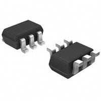
Pin Connections and Package Marking
SOURCE SOURCE GATE DRAIN SOURCE SOURCE
Surface Mount Package SOT-363 (SC-70)
Note: Top View. Package marking provides orientation and identification. “ 36 “ = Device code ATF-36163 Pin Conn “ x “ = Data code character
ATF-36163 Pkg
36x
Attention: Observe precautions for handling electrostatic sensitive devices. ESD Machine Model (Class A) Refer to Avago Application Note A004R: Electrostatic Discharge Damage and Control.
�ATF-36163 Absolute Maximum Ratings[1]
Symbol
VDS VGS VGD ID PT Pin max TCH TSTG
Parameter
Drain - Source Voltage Gate - Source Voltage Gate Drain Voltage Drain Current Total Power Dissipation RF Input Power Channel Temperature Storage Temperature
Units
V V V mA mW dBm °C °C
Absolute Maximum
+3 -3 -3.5 Idss 180 +10 150 -65 to 150
Thermal Resistance: θch-c = 160°C/W
Note: 1. Operation of this device above any one of these parameters may cause permanent damage.
ATF-36163 Electrical Specifications TC = 25°C, ZO = 50 Ω, Vds = 1.5 V, Ids = 10 mA, (unless otherwise noted).
Symbol
NF G gm Idss Vp 10% BVGDO
Parameters and Test Conditions
Noise Figure[1] Gain at NF[1] Transconductance Saturated Drain Current Pinchoff Voltage Gate Drain Breakdown Voltage f =12.0 GHz f = 12.0 GHz VDS = 1.5 V, VGS = 0 V VDS = 1.5 V, VGS = 0 V VDS = 1.5 V, IDS = 10% of Idss IG = 30 µA
Units
dB dB mS mA V V
Min.
9 50 15 -1.0
Typ.
1.2 10 60 25 -0.35
Max.
1.4[1]
40 -0.15 -3.5
Note: 1. Measured in a test circuit tuned for a typical device.
ATF-36163 Typical Parameters TC = 25°C, ZO = 50 Ω, Vds = 2 V, Ids = 15 mA, (unless otherwise noted).
Symbol
Fmin Ga Gmax P1dB VGS
Parameters and Test Conditions
Minimum Noise Figure (Γsource = Γopt) Associated Gain Maximum Available Gain[1] Output Power at 1 dB Gain Compression under the power matched condition Gate to Source Voltage for IDS = 15 mA f = 4 GHz f = 12 GHz f = 4 GHz f = 12 GHz f = 4 GHz f = 12 GHz f = 4 GHz f = 12 GHz VDS = 2.0 V
Units
dB dB dB dB dB dB dBm dBm V
Typ.
0.6 1.0 15.8 9.4 17.2 10.9 5 5 -0.2
Note: 1. Gmax = MAG for K > 1 and Gmax = MSG for K ≤ 1, which is shown on the S-parameters tables.
2
�ATF-36163 Typical Scattering Parameters, Common Source, ZO = 50 Ω, VDS = 1.5 V, ID = 10 mA
Freq. GHz
0.5 1 2 3 4 5 6 7 8 9 10 11 12 13 14 15 16 17 18
Mag.
0.99 0.98 0.96 0.93 0.87 0.81 0.75 0.67 0.61 0.57 0.57 0.59 0.63 0.67 0.72 0.78 0.82 0.87 0.90
S11
Ang.
-11 -22 -42 -61 -83 -106 -131 -158 176 143 108 76 50 26 6 -11 -24 -38 -52
dB
12.85 12.70 12.48 12.37 12.30 12.16 11.94 11.47 11.01 10.47 9.66 8.53 7.39 6.10 4.81 3.49 2.20 0.59 -1.63
S21 Mag.
4.39 4.31 4.21 4.15 4.12 4.06 3.95 3.75 3.55 3.34 3.04 2.67 2.34 2.02 1.74 1.50 1.29 1.07 0.83
Ang.
168 158 138 118 97 76 55 33 12 -10 -32 -54 -74 -93 -111 -128 -146 -164 178
dB
-37.72 -31.70 -26.02 -22.73 -20.45 -18.71 -17.52 -16.77 -16.36 -15.97 -15.92 -16.48 -17.14 -18.27 -19.74 -21.41 -23.10 -25.04 -29.12
S12 Mag.
0.01 0.03 0.05 0.07 0.10 0.12 0.13 0.15 0.15 0.16 0.16 0.15 0.14 0.12 0.10 0.09 0.07 0.06 0.04
Ang.
79 71 55 40 23 6 -12 -30 -45 -61 -77 -93 -106 -119 -129 -138 -144 -151 -159
Mag.
0.51 0.50 0.48 0.45 0.40 0.34 0.27 0.18 0.10 0.12 0.22 0.33 0.41 0.49 0.56 0.63 0.67 0.73 0.78
S22
Ang.
-9 -18 -36 -53 -71 -92 -116 -144 174 93 53 28 9 -8 -22 -33 -43 -53 -65
K —
0.11 0.17 0.24 0.33 0.43 0.51 0.58 0.69 0.79 0.85 0.91 0.99 1.07 1.18 1.30 1.38 1.44 1.46 1.80
Gmax[1] dB
25.24 22.26 19.28 17.56 16.38 15.43 14.73 14.12 13.69 13.22 12.80 12.50 10.65 9.64 8.99 8.81 8.70 8.79 8.58
Note: 1. Gmax = MAG for K > 1 and Gmax = MSG for K ≤ 1.
2.4 2.0
24 20 16 12 8 4 0 10 12 14 16 18
Ga (dB)
Common Source, ZO = 50 Ω, VDS = 1.5 V, ID = 10 mA Freq. GHz
2 3 4 5 6 7 8 9 10 11 12 13 14 15 16 17 18
Fmin (dB)
ATF-36163 Typical Noise Parameters
Fmin dB
0.48 0.53 0.57 0.61 0.66 0.71 0.77 0.83 0.89 0.97 1.05 1.14 1.24 1.37 1.51 1.68 1.89
1.6 1.2 0.8 0.4 0
Ga dB
18.77 16.75 15.17 14.14 13.23 12.06 11.22 10.50 10.02 9.44 8.92 8.45 8.12 8.08 8.11 7.97 7.59
Mag.
0.78 0.75 0.68 0.60 0.55 0.48 0.38 0.32 0.23 0.18 0.20 0.26 0.36 0.48 0.59 0.64 0.70
Γopt
Ang.
28 41 55 71 88 105 119 138 170 -141 -92 -46 -16 4 19 34 51
Rn/ZO 0.38 0.32 0.26 0.20 0.15 0.12 0.10 0.07 0.07 0.09 0.13 0.21 0.32 0.44 0.60 0.79 1.15
0
2
4
6
8
FREQUENCY (GHz)
Figure 1. ATF-36163 Minimum Noise Figure and Associated Gain vs. Frequency for VDS = 1.5 V, ID = 10 mA.
24 20 16
GAIN (dB)
ATF-36163 fig 1
MSG MAG |S21|2
12 8 4 0
0
2
4
6
8
10 12 14 16 18
FREQUENCY (GHz)
Figure 2. Maximum Available Gain, Maximum Stable Gain & Insertion Power Gain vs. Frequency for VDS = 1.5 V, ID = 10 mA.
ATF-36163 fig 2
3
�ATF-36163 Typical Scattering Parameters, Common Source, ZO = 50 Ω, VDS = 1.5 V, ID = 15 mA
Freq. GHz
0.5 1 2 3 4 5 6 7 8 9 10 11 12 13 14 15 16 17 18
Mag.
0.99 0.98 0.96 0.92 0.86 0.80 0.74 0.66 0.59 0.56 0.56 0.59 0.63 0.68 0.73 0.79 0.83 0.87 0.91
S11
Ang.
-12 -22 -43 -63 -85 -108 -133 -160 173 141 106 74 49 25 5 -12 -25 -38 -53
dB
13.56 13.40 13.16 13.00 12.87 12.68 12.38 11.85 11.33 10.74 9.89 8.74 7.59 6.29 5.01 3.70 2.43 0.84 -1.33
S21 Mag.
4.76 4.68 4.55 4.47 4.40 4.30 4.16 3.91 3.68 3.44 3.12 2.74 2.40 2.06 1.78 1.53 1.32 1.10 0.86
Ang.
168 157 137 116 96 75 53 31 11 -11 -33 -54 -74 -93 -110 -127 -144 -163 180
dB
-38.42 -32.40 -26.56 -23.22 -21.01 -19.25 -18.13 -17.39 -16.95 -16.54 -16.42 -16.83 -17.39 -18.42 -19.74 -21.31 -22.85 -24.73 -28.87
S12 Mag.
0.01 0.02 0.05 0.07 0.09 0.11 0.12 0.14 0.14 0.15 0.15 0.14 0.14 0.12 0.10 0.09 0.07 0.06 0.04
Ang.
79 71 56 40 24 7 -11 -28 -42 -58 -73 -88 -102 -115 -124 -133 -139 -148 -155
Mag.
0.45 0.45 0.43 0.40 0.35 0.28 0.21 0.13 0.06 0.12 0.23 0.34 0.42 0.50 0.57 0.64 0.68 0.73 0.78
S22
Ang.
-9 -18 -36 -52 -70 -92 -116 -146 156 73 44 23 6 -10 -23 -34 -44 -54 -66
K —
0.12 0.18 0.26 0.35 0.46 0.55 0.62 0.74 0.84 0.90 0.95 1.03 1.10 1.19 1.29 1.35 1.39 1.39 1.67
Gmax[1] dB
25.82 22.86 19.87 18.13 16.94 15.98 15.25 14.62 14.14 13.63 13.16 11.78 10.62 9.72 9.15 8.99 8.93 9.06 8.92
Note: 1. Gmax = MAG for K > 1 and Gmax = MSG for K ≤ 1.
2.4 2.0
24 20 16 12 8 4 0 10 12 14 16 18
Ga (dB)
Common Source, ZO = 50 Ω, VDS = 1.5 V, ID = 15 mA Freq. GHz
2 3 4 5 6 7 8 9 10 11 12 13 14 15 16 17 18
Fmin (dB)
ATF-36163 Typical Noise Parameters
Fmin dB
0.49 0.54 0.58 0.63 0.68 0.73 0.79 0.85 0.91 0.99 1.07 1.17 1.27 1.40 1.54 1.72 1.93
1.6 1.2 0.8 0.4 0
Ga dB
18.87 17.20 15.75 14.49 13.61 12.36 11.54 10.82 10.32 9.73 9.22 8.68 8.41 8.36 8.37 8.10 8.00
Mag.
0.84 0.74 0.66 0.59 0.54 0.46 0.37 0.30 0.21 0.17 0.20 0.26 0.38 0.49 0.60 0.62 0.71
Γopt
Ang.
28 42 57 72 90 106 121 140 174 -133 -83 -40 -12 7 21 35 52
Rn/ZO 0.38 0.31 0.25 0.19 0.15 0.11 0.09 0.08 0.08 0.10 0.14 0.22 0.34 0.46 0.64 0.85 1.18
0
2
4
6
8
FREQUENCY (GHz)
Figure 3. ATF-36163 Minimum Noise Figure and Associated Gain vs. Frequency for VDS = 1.5 V, ID = 15 mA.
24 20 16
GAIN (dB)
ATF-36163 fig 3
MSG MAG |S21|2
12 8 4 0
0
2
4
6
8
10 12 14 16 18
FREQUENCY (GHz)
Figure 4. Maximum Available Gain, Maximum Stable Gain & Insertion Power Gain vs. Frequency for VDS = 1.5 V, ID = 15 mA.
ATF-36163 fig 4
4
�ATF-36163 Typical Scattering Parameters, Common Source, ZO = 50 Ω, VDS = 2.0 V, ID = 10 mA
Freq. GHz
0.5 1 2 3 4 5 6 7 8 9 10 11 12 13 14 15 16 17 18
Mag.
0.99 0.99 0.96 0.93 0.87 0.81 0.75 0.67 0.60 0.57 0.56 0.58 0.62 0.67 0.72 0.78 0.82 0.87 0.91
S11
Ang.
-11 -22 -42 -62 -83 -106 -131 -157 176 144 109 77 50 26 6 -10 -24 -37 -52
dB
13.06 12.90 12.69 12.57 12.51 12.38 12.15 11.70 11.25 10.73 9.95 8.86 7.75 6.49 5.24 3.96 2.68 1.08 -1.16
S21 Mag.
4.50 4.42 4.31 4.25 4.22 4.16 4.05 3.84 3.65 3.44 3.14 2.77 2.44 2.11 1.83 1.58 1.36 1.13 0.88
Ang.
168 158 138 118 97 76 55 33 13 -10 -32 -53 -73 -93 -110 -128 -146 -165 177
dB
-37.72 -32.04 -26.38 -22.97 -20.72 -18.94 -17.79 -17.08 -16.65 -16.25 -16.25 -16.77 -17.39 -18.56 -19.91 -21.51 -23.10 -24.88 -28.64
S12 Mag.
0.01 0.03 0.05 0.07 0.09 0.11 0.13 0.14 0.15 0.15 0.15 0.15 0.14 0.12 0.10 0.08 0.07 0.06 0.04
Ang.
79 71 56 40 23 6 -12 -30 -44 -60 -76 -91 -104 -117 -126 -134 -139 -147 -153
Mag.
0.55 0.55 0.53 0.50 0.44 0.38 0.31 0.21 0.13 0.10 0.18 0.29 0.37 0.46 0.53 0.60 0.65 0.71 0.78
S22
Ang.
-9 -18 -35 -52 -70 -90 -112 -137 -168 115 61 32 12 -5 -19 -30 -40 -50 -63
K –
0.11 0.16 0.24 0.32 0.42 0.51 0.58 0.69 0.79 0.85 0.91 1.00 1.08 1.19 1.31 1.38 1.42 1.38 1.63
Gmax[1] dB
25.46 22.46 19.50 17.77 16.61 15.67 14.98 14.38 13.96 13.50 13.10 12.52 10.82 9.85 9.24 9.07 9.03 9.28 9.06
Note: 1. Gmax = MAG for K > 1 and Gmax = MSG for K ≤ 1.
2.4 2.0 24 20 16 12 8 4 0 10 12 14 16 18
Ga (dB)
Fmin (dB)
ATF-36163 Typical Noise Parameters
Freq. GHz
2 3 4 5 6 7 8 9 10 11 12 13 14 15 16 17 18
1.6 1.2 0.8 0.4 0
Common Source, ZO = 50 Ω, VDS = 2.0 V, ID = 10 mA Fmin dB
0.46 0.50 0.54 0.59 0.63 0.68 0.74 0.80 0.86 0.94 1.02 1.11 1.22 1.35 1.51 1.69 1.92
Ga dB
18.60 16.75 15.55 14.20 13.37 12.12 11.35 10.59 10.11 9.57 9.08 8.59 8.30 8.29 8.32 8.07 7.68
Mag.
0.84 0.76 0.67 0.61 0.55 0.49 0.39 0.33 0.23 0.17 0.18 0.24 0.34 0.47 0.58 0.60 0.66
Γopt
Ang.
28 41 56 70 88 103 118 135 165 -145 -93 -47 -16 5 19 34 50
Rn/ZO 0.38 0.31 0.25 0.20 0.15 0.12 0.10 0.07 0.07 0.09 0.12 0.19 0.30 0.42 0.57 0.76 1.10
0
2
4
6
8
FREQUENCY (GHz)
Figure 5. ATF-36163 Minimum Noise Figure and Associated Gain vs. Frequency for VDS = 2.0 V, ID = 10 mA.
24 20 16
GAIN (dB)
ATF-36163 fig 5
MSG MAG
12 8 4 0 |S21|2
0
2
4
6
8
10 12 14 16 18
FREQUENCY (GHz)
Figure 6. Maximum Available Gain, Maximum Stable Gain & Insertion Power Gain vs. Frequency for VDS = 2.0 V, ID = 10 mA.
ATF-36163 fig 6
5
�ATF-36163 Typical Scattering Parameters, Common Source, ZO = 50 Ω, VDS = 2 V, ID = 15 mA
Freq. GHz
0.5 1 2 3 4 5 6 7 8 9 10 11 12 13 14 15 16 17 18
Mag.
0.99 0.98 0.96 0.92 0.86 0.79 0.73 0.65 0.59 0.55 0.56 0.58 0.63 0.68 0.73 0.78 0.83 0.88 0.91
S11
Ang.
-12 -22 -43 -63 -85 -108 -133 -160 173 141 107 75 49 26 6 -11 -24 -38 -52
dB
13.85 13.70 13.45 13.29 13.16 12.96 12.67 12.13 11.63 11.06 10.23 9.11 8.00 6.75 5.49 4.22 2.99 1.42 -0.79
S21 Mag.
4.93 4.84 4.70 4.62 4.55 4.45 4.30 4.04 3.81 3.57 3.25 2.86 2.51 2.17 1.88 1.63 1.41 1.18 0.91
Ang.
168 157 137 117 96 75 53 32 11 -11 -32 -53 -73 -92 -110 -127 -145 -164 178
dB
-38.42 -32.40 -26.74 -23.48 -21.31 -19.58 -18.42 -17.72 -17.27 -16.83 -16.77 -17.14 -17.72 -18.71 -20.00 -21.41 -22.73 -24.44 -27.96
S12 Mag.
0.01 0.02 0.05 0.07 0.09 0.11 0.12 0.13 0.14 0.14 0.15 0.14 0.13 0.12 0.10 0.09 0.07 0.06 0.04
Ang.
79 71 56 40 24 7 -10 -28 -42 -57 -72 -87 -99 -112 -121 -129 -135 -143 -149
2.4 2.0 1.6
Mag.
0.51 0.50 0.48 0.45 0.40 0.33 0.26 0.17 0.09 0.09 0.19 0.30 0.38 0.47 0.54 0.61 0.66 0.72 0.78
S22
Ang.
-9 -18 -35 -52 -69 -90 -112 -136 -171 93 51 27 9 -7 -20 -31 -41 -51 -63
K –
0.12 0.17 0.26 0.35 0.46 0.55 0.62 0.75 0.84 0.90 0.96 1.04 1.11 1.20 1.30 1.35 1.36 1.31 1.50
Gmax[1] dB
26.10 23.11 20.13 18.40 17.22 16.26 15.54 14.93 14.46 13.95 13.50 11.93 10.85 10.00 9.45 9.30 9.31 9.56 9.44
24 20 16 12 8 4
Ga (dB)
Note: 1. Gmax = MAG for K > 1 and Gmax = MSG for K ≤ 1.
ATF-36163 Typical Noise Parameters
Freq. GHz
2 3 4 5 6 7 8 9 10 11 12 13 14 15 16 17 18
Fmin (dB)
Common Source, ZO = 50 Ω, VDS = 2.0 V, ID = 15 mA Fmin dB
0.48 0.52 0.56 0.61 0.65 0.70 0.76 0.82 0.88 0.95 1.03 1.12 1.23 1.35 1.49 1.65 1.86
1.2 0.8 0.4 0
Ga dB
18.97 17.27 15.75 14.54 13.68 12.47 11.66 10.94 10.44 9.88 9.38 8.90 8.63 8.59 8.63 8.68 8.32
Mag.
0.83 0.74 0.67 0.60 0.55 0.46 0.37 0.31 0.21 0.15 0.18 0.25 0.36 0.48 0.58 0.65 0.70
Γopt
Ang.
28 41 56 71 89 104 118 136 168 -137 -85 -41 -13 7 20 34 51
Rn/ZO 0.37 0.31 0.25 0.19 0.15 0.11 0.09 0.08 0.07 0.09 0.13 0.21 0.32 0.44 0.60 0.79 1.10
0
2
4
6
8
0 10 12 14 16 18
FREQUENCY (GHz)
Figure 7. ATF-36163 Minimum Noise Figure and Associated Gain vs. Frequency for VDS = 2 V, ID = 15 mA.
24 20 16
GAIN (dB)
ATF-36163 fig 7
MSG MAG
12 8 4 0 |S21|2
0
2
4
6
8
10 12 14 16 18
FREQUENCY (GHz)
Figure 8. Maximum Available Gain, Maximum Stable Gain & Insertion Power Gain vs. Frequency for VDS = 2 V, ID = 15 mA.
ATF-36163 fig 8
6
�ATF-36163 Typical “Off” Scattering Parameters, Common Source, ZO = 50 Ω, VDS = 0 V, VGS = 0 V
Freq. GHz
0.5 1 2 3 4 5 6 7 8 9 10 11 12 13 14 15 16 17 18
Mag.
0.998 0.993 0.99 0.98 0.96 0.94 0.92 0.89 0.86 0.84 0.83 0.83 0.85 0.86 0.87 0.90 0.93 0.93 0.93
S11
Ang.
-10 -20 -37 -55 -74 -95 -118 -142 -168 162 128 94 64 36 12 -8 -24 -39 -53
dB
-46.02 -39.17 -32.77 -28.64 -25.35 -22.62 -20.45 -18.79 -17.02 -15.70 -14.85 -14.66 -14.85 -15.76 -17.14 -18.71 -20.45 -23.35 -27.96
S21 Mag.
0.01 0.01 0.02 0.04 0.05 0.07 0.10 0.12 0.14 0.16 0.18 0.19 0.18 0.16 0.14 0.12 0.10 0.07 0.04
Ang.
80 81 75 67 56 42 27 11 -6 -24 -44 -64 -83 -101 -116 -129 -140 -154 -161
dB
-46.02 -39.17 -32.77 -28.64 -25.19 -22.50 -20.45 -18.71 -17.02 -15.70 -14.85 -14.66 -14.85 -15.76 -17.08 -18.71 -20.45 -23.10 -28.18
S12 Mag.
0.01 0.01 0.02 0.04 0.06 0.08 0.10 0.12 0.14 0.16 0.18 0.19 0.18 0.16 0.14 0.12 0.10 0.07 0.04
Ang.
86 83 76 68 57 42 27 11 -5 -24 -44 -64 -83 -101 -115 -129 -140 -152 -161
Mag.
0.703 0.701 0.70 0.71 0.73 0.74 0.75 0.77 0.78 0.81 0.83 0.84 0.85 0.87 0.89 0.89 0.90 0.90 0.90
S22
Ang.
170 160 139 119 99 81 63 46 30 16 3 -10 -22 -34 -44 -53 -62 -71 -81
ATF-36163 Typical “Off” Scattering Parameters, Common Source, ZO = 50 Ω, VDS = 2.0 V, VGS = -1.5 V
Freq. GHz
0.5 1 2 3 4 5 6 7 8 9 10 11 12 13 14 15 16 17 18
Mag.
0.97 0.98 0.99 0.98 0.97 0.96 0.94 0.92 0.89 0.85 0.79 0.74 0.72 0.71 0.75 0.82 0.89 0.91 0.92
S11
Ang.
-8 -16 -30 -43 -57 -72 -87 -103 -119 -136 -158 177 149 114 74 35 5 -21 -42
dB
-34.89 -28.87 -22.85 -19.33 -16.71 -14.42 -12.62 -10.90 -9.60 -8.09 -6.73 -5.85 -5.71 -6.54 -8.95 -12.80 -18.49 -24.88 -27.54
S21 Mag.
0.02 0.04 0.07 0.11 0.15 0.19 0.23 0.29 0.33 0.39 0.46 0.51 0.52 0.47 0.36 0.23 0.12 0.06 0.04
Ang.
82 74 59 44 29 14 -2 -20 -37 -56 -79 -106 -136 -170 155 123 94 79 70
dB
-34.89 -28.87 -22.97 -19.33 -16.71 -14.47 -12.65 -10.96 -9.63 -8.09 -6.73 -5.87 -5.71 -6.52 -8.92 -12.69 -18.20 -24.44 -27.96
S12 Mag.
0.02 0.04 0.07 0.11 0.15 0.19 0.23 0.28 0.33 0.39 0.46 0.51 0.52 0.47 0.36 0.23 0.12 0.06 0.04
Ang.
81 73 59 44 30 14 -2 -20 -37 -56 -79 -106 -136 -170 156 123 95 84 69
Mag.
0.999 0.998 0.995 0.98 0.97 0.95 0.94 0.92 0.89 0.83 0.79 0.75 0.73 0.74 0.79 0.85 0.90 0.91 0.90
S22
Ang.
-7 -14 -29 -43 -57 -74 -91 -107 -125 -148 -174 156 123 86 50 18 -8 -30 -50
7
�1.9 dB 1.4 dB 1.3 dB 1.2 dB 1.1 dB
9.5 dB 10.5 dB
11.5 dB
Figure 9. Smith Chart with Noise Figure and Available Gain Circles at 12 GHz, VDS = 1.5 V, ID = 10 mA.
Phase Reference Planes
ATF-36163 fig 9 The positions of the reference planes used to measure SParameters and to specify Γopt for the Noise Parameters are shown in Figure 10. As seen in the illustration, the reference planes are located at the extremities of the package leads.
REFERENCE PLANES
SOT-363 PCB Layout
A PCB pad layout for the miniature SOT-363 (SC-70) package used by the ATF-36163 is shown in Figure 11 (dimensions are in inches). This layout provides ample allowance for package placement by automated assembly equipment. The layout is shown with a nominal SOT-363 package footprint superimposed on the PCB. pads.
0.026
TEST CIRCUIT
0.079
Figure 10. Reference Planes.
0.039
MGA-86563 fig 11
0.018 Dimensions in inches.
Figure 11. Recommended PCB Pad Layout for Avago’s SC70 6L/SOT-363 Products (Dimensions in Inches).
8
�Package Dimensions
SC-70 6L/SOT-363
HE
E
e D
Q1 A2 A1 b L A c
DIMENSIONS (mm) SYMBOL E D HE A A2 A1 Q1 e b c L MIN. 1.15 1.80 1.80 0.80 0.80 0.00 0.10 0.650 BCS 0.15 0.10 0.10 0.30 0.20 0.30 MAX. 1.35 2.25 2.40 1.10 1.00 0.10 0.40
NOTES: 1. All dimensions are in mm. 2. Dimensions are inclusive of plating. 3. Dimensions are exclusive of mold flash & metal burr. 4. All specifications comply to EIAJ SC70. 5. Die is facing up for mold and facing down for trim/form, ie: reverse trim/form. 6. Package surface to be mirror finish.
Part Number Ordering Information
Part Number
ATF-36163-TR1G ATF-36163-TR2G ATF-36163-BLKG
No. of Devices
3000 10000 100
Container
7” Reel 13” Reel antistatic bag
9
�Device Orientation
REEL
TOP VIEW 4 mm END VIEW
8 mm
CARRIER TAPE USER FEED DIRECTION COVER TAPE
36
36
36
36
Tape Dimensions and Product Orientation For Outline 63
P P0 D P2 ATF-36163 Tape – Device Orientation
ATF-36163 Device Orientation
E
F W C
t1 (CARRIER TAPE THICKNESS)
D1
Tt (COVER TAPE THICKNESS)
10° MAX.
K0
10° MAX.
A0
B0
DESCRIPTION CAVITY LENGTH WIDTH DEPTH PITCH BOTTOM HOLE DIAMETER DIAMETER PITCH POSITION WIDTH THICKNESS WIDTH TAPE THICKNESS CAVITY TO PERFORATION (WIDTH DIRECTION) CAVITY TO PERFORATION (LENGTH DIRECTION)
SYMBOL A0 B0 K0 P D1 D P0 E W t1 C Tt F P2
SIZE (mm) 2.40 ± 0.10 2.40 ± 0.10 1.20 ± 0.10 4.00 ± 0.10 1.00 + 0.25 1.55 ± 0.10 4.00 ± 0.10 1.75 ± 0.10 8.00 + 0.30 - 0.10 0.254 ± 0.02 5.40 ± 0.10 0.062 ± 0.001 3.50 ± 0.05 2.00 ± 0.05
SIZE (INCHES) 0.094 ± 0.004 0.094 ± 0.004 0.047 ± 0.004 0.157 ± 0.004 0.039 + 0.010 0.061 + 0.002 0.157 ± 0.004 0.069 ± 0.004 0.315 + 0.012 0.0100 ± 0.0008 0.205 + 0.004 0.0025 ± 0.0004 0.138 ± 0.002 0.079 ± 0.002
PERFORATION
CARRIER TAPE COVER TAPE DISTANCE
For product information and a complete list of distributors, please go to our web site:
www.avagotech.com
Avago, Avago Technologies, and the A logo are trademarks of Avago Technologies in the United States and other countries. Data subject to change. Copyright © 2005-2008 Avago Technologies. All rights reserved. Obsoletes 5989-1915EN AV02-1441EN - July 29, 2008
�


 工商网监
湘ICP备2023018690号
工商网监
湘ICP备2023018690号
