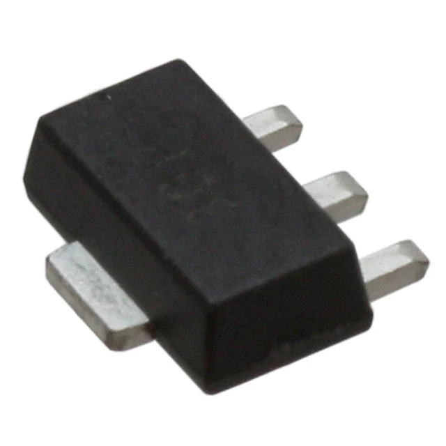
ATF-52189
High Linearity Mode[1] Enhancement
Pseudomorphic HEMT in SOT 89 Package
Data Sheet
Description
Features
Avago Technologies’s ATF-52189 is a single-voltage high
linearity, low noise E-pHEMT FET packaged in a low cost
surface mount SOT89 package. The device is ideal as a
medium-power, high-linearity amplifier. Its operating frequency range is from 50 MHz to 6 GHz.
• Single voltage operation
ATF-52189 is ideally suited for Cellular/PCS and WCDMA
wireless infrastructure, WLAN, WLL and MMDS application, and general purpose discrete E-pHEMT amplifiers
which require medium power and high linearity. All devices are 100% RF and DC tested.
• SOT 89 standard package
Notes:
1. Enhancement mode technology employs a single positive Vgs,
eliminating the need of negative gate voltage associated with
conventional depletion mode devices.
2. Refer to reliability datasheet for detailed MTTF data
3. Conform to JEDEC reference outline MO229 for DRP-N
4. Linearity Figure of Merit (LFOM) is OIP3 divided by DC bias power
• High Linearity and P1dB
• Low Noise Figure
• Excellent uniformity in product specifications
• Point MTTF > 300 years[2]
• MSL-2 and lead-free
• Tape-and-Reel packaging option available
Specifications
2 GH, 4.5V, 280 mA (Typ.)
• 42 dBm Output IP3
• 27 dBm Output Power at 1dB gain compression
• 1.50 dB Noise Figure
• 16.0 dB Gain
• 55% PAE at P1dB
Pin Connections and Package Marking
• LFOM[3] 12.5 dB
Applications
• Front-end LNA Q2 and Q3, Driver or Pre-driver Amplifier
for Cellular/PCS and WCDMA wireless infrastructure
2GX
#1
#2
RFin
GND
Top View
• Driver Amplifier for WLAN, WLL/RLL and MMDS
applications
#3
RFout
#3
#2
RFout
GND
#1
RFin
Bottom View
Notes:
Package marking provides orientation and identification:
“2G” = Device Code
“x” = Month code indicates the month of manufacture.
• General purpose discrete E-pHEMT for other high
linearity applications
�ATF-52189 Absolute Maximum Ratings[1]
Symbol
Parameter
Units
Absolute
Maximum
Vds
Drain–Source Voltage[2]
V
7
Vgs
Gate–Source Voltage[2]
V
-5 to 1.0
Vgd
Gate Drain Voltage[2]
V
-5 to 1.0
Ids
Drain Current[2]
mA
500
Igs
Gate Current
mA
46
Pdiss
Total Power Dissipation[3]
W
1.5
Pin max.
RF Input Power
dBm
+27
Tch
Channel Temperature
°C
150
Tstg
Storage Temperature
°C
-65 to 150
Thermal Resistance[2,4]
θch-b = 52°C/W
Notes:
1. Operation of this device above any one of
these parameters may cause permanent
damage.
2. Assuming DC quiescent conditions.
3. Board (package belly) temperature TB is 25°C.
Derate 19.25 mW/°C for TB > 72°C.
4. Channel-to-board thermal resistance
measured using 150°C Liquid Crystal
Measurement method.
ATF-52189 Electrical Specifications
TA = 25°C, DC bias for RF parameters is Vds = 4.5V and Ids = 200 mA unless otherwise specified.
Symbol
Parameters and Test Conditions
Units
Min.
Typ.
Max.
Vgs
Operational Gate Voltage
V
—
0.62
—
Vth
Threshold Voltage
Vds = 4.5V, Ids = 16 mA
V
Ids
Drain to Source Current
Vds = 4.5V, Vgs = 0V
μA
—
0.28
—
—
14.8
—
Gm
Transconductance
Vds = 4.5V, Gm = ΔIds/ΔVgs;
ΔVgs = Vgs1 – Vgs2
Vgs1 = 0.55V, Vgs2 = 0.5V
mmho
—
1300
—
Igss
Gate Leakage Current
Vds = 0V, Vgs = -4V
μA
-20.0
0.49
—
NF
Noise Figure
f = 2 GHz
f = 900 MHz
dB
dB
—
—
1.50
1.25
—
—
G
Gain [1]
f = 2 GHz
f = 900 MHz
dB
dB
14.8
—
16.0
16.5
17.8
—
OIP3
Output 3rd Order Intercept Point [1]
f = 2 GHz
f = 900 MHz
dBm
dBm
38.5
—
42.0
42.0
—
—
P1dB
Output 1dB Compressed[1]
f = 2 GHz
f = 900 MHz
dBm
dBm
25.5
—
27.0
27.2
—
—
PAE
Power Added Efficiency
f = 2 GHz
f = 900 MHz
%
%
40.0
—
55.0
50.0
—
—
NF
Noise Figure
f=900 MHz
f=2.0 GHz
f=2.4 GHz
dB
dB
dB
—
—
—
1.25
1.50
1.60
—
—
—
G
Gain [1]
f=900 MHz
f=2.0 GHz
f=2.4 GHz
dB
dB
dB
—
14.8
—
16.5
16.0
13.5
—
17.8
—
OIP3
Output 3rd Order Intercept Point [1]
f=900 MHz
f=2.0 GHz
f=2.4 GHz
dBm
dBm
dBm
—
38.5
—
42.0
42.0
41.0
—
—
—
P1dB
Output 1dB Compressed [1]
f=900 MHz
f=2.0 GHz
f=2.4 GHz
dBm
dBm
dBm
—
25.5
—
27.2
27.0
26.0
—
—
Vds = 4.5V, Ids = 200 mA
continued on next page
22
�Symbol
Parameters and Test Conditions
PAE
Power Added Efficiency
ACLR
Adjacent Channel Leakage
Power Ratio [1,2]
Units
Min.
Typ.
Max.
f=900 MHz
f=2.0 GHz
f=2.4 GHz
%
%
%
—
40.0
—
50.0
55.0
52.0
—
—
Offset BW = 5 MHz
Offset BW = 10 MHz
dBc
dBc
—
—
-58.0
-66.0
—
—
Notes:
1. Measurements at 2 GHz obtained using production test board described in Figure 1.
2. ACLR test spec is based on 3GPP TS 25.141 V5.3.1 (2002-06)
- Test Model 1
- Active Channels: PCCPCH + SCH + CPICH + PICH + SCCPCH + 64 DPCH (SF=128)
- Freq = 2140 MHz
- Pin = -8 dBm
- Channel Integrate Bandwidth = 3.84 MHz
Input Matching Circuit
Γ_mag=0.76
Γ_ang=-131.3°
Input
Output Matching Circuit
Γ_mag=0.32
Γ_ang=-176.6°
DUT
Output
Figure 1. Block diagram of the 2 GHz production test board used for NF, Gain, OIP3 , P1dB, PAE
and ACLR measurements. This circuit achieves a trade-off between optimal OIP3, P1dB and
VSWR. Circuit losses have been de-embedded from actual measurements.
Product Consistency Distribution Charts [1,2]
150
150
Stdev=0.30
Stdev=0.35
120
90
–3 Std
+3 Std
60
FREQUENCY
FREQUENCY
120
90
–3 Std
60
30
30
0
41.5
42
42.5
43
0
43.5
26.25
26.75
28.25
150
150
Stdev=0.10
Stdev=0.16
120
90
–3 Std
FREQUENCY
120
FREQUENCY
27.75
Figure 3. P1dB @ 2 GHz, 4.5V, 200 mA.
LSL = 25.5 dBm, Nominal = 27.1 dBm.
Figure 2. OIP3 @ 2 GHz, 4.5V/200 mA.
LSL = 38.5 dBm, Nominal = 42.4 dBm.
+3 Std
60
0
15.5
90
–3 Std
+3 Std
60
30
30
0
16
16.5
GAIN (dBm)
Figure 4. Gain @ 2 GHz, 4.5V, 200 mA.
LSL = 14.8 dBm, Nominal = 16.1 dBm,
USL = 17.8 dB.
3
27.25
P1dB (dBm)
OIP3 (dBm)
3
+3 Std
17
1
1.25
1.5
1.75
NF (dBm)
Figure 5. NF @ 2 GHz, 4.5V, 200 mA.
Nominal = 1.5 dBm.
2
Notes:
1. Distribution data sample size is 500 samples
taken from 3 different wafers. Future wafers
allocated to this product may have nominal
values anywhere between the upper and
lower limits.
2. Measurements are made on production test
board, which represents a trade-off between
optimal OIP3, P1dB and VSWR. Circuit losses
have been de-embedded from actual
measurements.
�Gamma Load and Source at Optimum OIP3 and P1dB Tuning Conditions
The device’s optimum OIP3 and P1dB measurements were determined using a Maury Load Pull System at
4.5V, 200 mA quiesent bias.
Typical Gammas at Optimum OIP3 [1]
Freq
(GHz)
Gamma Source
Mag
Ang (deg)
Gamma Load
Mag
Ang (deg)
OIP3
(dBm)
Gain
(dB)
P1dB
(dBm)
PAE
(%)
0.9
0.7511
-132.82
0.6444
-157.38
42.0
16.5
27.2
49.7
2.0
0.7577
-131.31
0.3236
-176.55
42.0
15.7
26.8
54.9
2.4
0.7625
-128.49
0.2665
-148.09
41.0
13.6
26.5
49.5
3.9
0.7432
-94.91
0.4125
-98.27
40.0
10.8
27.3
49.1
Typical Gammas at Optimum P1dB [1]
Freq
(GHz)
Gamma Source
Mag
Ang (deg)
Gamma Load
Mag
Ang (deg)
OIP3
(dBm)
Gain
(dB)
P1dB
(dBm)
PAE
(%)
0.9
0.7786
139.82
0.5494
-177.76
38.6
17.3
28.4
58.3
2.0
0.7052
-168.54
0.6981
-165.37
37.5
14.8
29.0
48.6
2.4
0.7117
-161.45
0.6624
-159.44
37.3
12.0
29.3
48.2
3.9
0.3379
-100.92
0.6151
-126.28
37.0
9.1
28.0
46.2
Note:
1. Typical describes additional product performance information that is not covered by the product warranty.
600
0.8V
500
0.7V
Ids (mA)
400
300
0.6V
200
0.5V
100
0.4V
0
0
1
2
3
4
Vds (V)
Figure 6. Typical IV Curve.
44
5
6
7
�45
45
40
40
40
35
35
35
25
3V
4V
4.5V
20
15
100
150
200
250
300
350
30
25
3V
4V
4.5V
20
15
100
400
150
200
15
100
400
18
18
13
17
17
12
16
15
14
300
350
13
12
100
400
150
200
Gain_3V
Pout_3V
PAE_3V
70
30
60
25
40
15
30
10
20
5
0
-10
-6
-2
2
6
10
14
PAE (%)
50
20
GAIN (dB) & Pout (dBm)
30
300
350
7
100
400
3V
4V
4.5V
150
200
Pin (dBm)
Note:
Bias current for the above charts are quiescent
conditions. Actual level may increase depending
on amount of RF drive.
30
60
25
50
30
10
0
-10
Figure 13. Small Signal Gain/Pout/PAE vs.
Pin at Vds = 3V and Frequency = 900 MHz.
Gain_4V
Pout_4V
PAE_4V
70
40
0
20
-6
-2
2
250
300
350
400
Figure 12. Small Signal Gain vs. Ids and
Vds at 3.9 GHz.
15
10
400
Ids (mA)
20
5
350
10
8
Figure 11. Small Signal Gain vs. Ids and
Vds at 2 GHz.
Figure 10. Small Signal Gain vs. Ids and
Vds at 900 MHz.
300
11
Ids (mA)
Ids (mA)
25
250
250
9
3V
4V
4.5V
6
10
14
GAIN (dB) & Pout (dBm)
250
15
PAE (%)
200
16
14
3V
4V
4.5V
13
GAIN (dB)
14
150
200
Figure 9. OIP3 vs. Ids and Vds at 3.9 GHz.
19
12
100
150
Ids (mA)
19
GAIN (dB)
GAIN (dB)
350
3V
4V
4.5V
20
Figure 8. OIP3 vs. Ids and Vds at 2 GHz.
Figure 7. OIP3 vs. Ids and Vds at 900 MHz.
GAIN (dB) & Pout (dBm)
300
25
Ids (mA)
Ids (mA)
55
250
30
60
50
40
15
30
10
10
0
0
-10
Pin (dBm)
Gain_4.5V
Pout_4.5V
PAE_4.5V
20
5
Figure 14. Small Signal Gain/Pout/PAE vs.
Pin at Vds = 4V and Frequency = 900 MHz.
70
20
10
-6
-2
2
6
10
14
0
Pin (dBm)
Figure 15. Small Signal Gain/Pout/PAE vs.
Pin at Vds = 4.5V and Frequency = 900 MHz.
PAE (%)
30
OIP3 (dBm)
45
OIP3 (dBm)
OIP3 (dBm)
ATF-52189 Typical Performance Curves (at 25°C unless specified otherwise)
Tuned for Optimal OIP3 at Vd = 4.5V, Ids = 200 mA.
�ATF-52189 Typical Performance Curves (at 25°C unless specified otherwise), continued
Tuned for Optimal OIP3 at Vd = 4.5V, Ids = 200 mA.
30
10
20
5
2
6
10
14
18
40
15
30
10
20
0
0
-10
-6
-2
30
Gain_3V
Pout_3V
PAE_3V
40
30
10
20
5
10
6
10
14
18
0
Pin (dBm)
Figure 19. Small Signal Gain/Pout/PAE vs.
Pin at Vds = 3V and Frequency = 3.9 GHz.
Note:
Bias current for the above charts are quiescent
conditions. Actual level may increase depending
on amount of RF drive.
66
GAIN (dB) & Pout (dBm)
60
2
18
50
40
15
30
10
20
0
0
-10
10
-6
-2
30
50
25
0
18
50
20
10
5
10
0
0
-10
5
14
Gain_4.5V
Pout_4.5V
PAE_4.5V
10
20
10
60
30
10
6
18
15
30
2
14
40
15
-2
10
20
40
-6
6
Figure 18. Small Signal Gain/Pout/PAE vs.
Pin at Vds = 4.5V and Frequency = 2 GHz.
60
20
0
-10
2
Pin (dBm)
Gain_4V
Pout_4V
PAE_4V
25
PAE (%)
GAIN (dB) & Pout (dBm)
70
15
-2
14
30
50
-6
10
Figure 17. Small Signal Gain/Pout/PAE vs.
Pin at Vds = 4V and Frequency = 2 GHz.
80
20
0
-10
6
60
20
Pin (dBm)
Pin (dBm)
Figure 16. Small Signal Gain/Pout/PAE vs.
Pin at Vds = 3V and Frequency = 2 GHz.
25
2
70
5
10
GAIN (dB) & Pout (dBm)
-2
50
5
10
-6
60
20
Gain_4.5V
Pout_4.5V
PAE_4.5V
25
Pin (dBm)
Figure 20. Small Signal Gain/Pout/PAE vs.
Pin at Vds = 4V and Frequency = 3.9 GHz.
PAE (%)
0
-10
70
PAE (%)
40
15
PAE (%)
50
GAIN (dB) & Pout (dBm)
60
20
Gain_4V
Pout_4V
PAE_4V
25
80
-6
-2
2
6
10
14
18
0
Pin (dBm)
Figure 21. Small Signal Gain/Pout/PAE vs.
Pin at Vds = 4.5V and Frequency = 3.9 GHz.
PAE (%)
70
30
80
PAE (%)
Gain_3V
Pout_3V
PAE_3V
25
GAIN (dB) & Pout (dBm)
30
80
GAIN (dB) & Pout (dBm)
30
�46
18
44
16
42
14
GAIN (dB)
OIP3 (dBm)
ATF-52189 Typical Performance Curves, continued
Tuned for Optimal OIP3 at Vd = 4.5V, Ids = 200 mA, Over Temperature and Frequency
40
38
10
-40°C
25°C
80°C
36
34
0.5
12
1
1.5
-40°C
25°C
80°C
8
2
2.5
3
3.5
6
0.5
4
1
FREQUENCY (GHz)
60
27.5
55
27
50
PAE (%)
28
P1dB (dBm)
2.5
3
3.5
4
Figure 23. Gain vs. Temperature and
Frequency at optimum OIP3.
26.5
26
45
40
-40°C
25°C
80°C
25.5
1
1.5
-40°C
25°C
80°C
35
2
2.5
3
3.5
4
FREQUENCY (GHz)
Figure 24. P1dB vs. Temperature and
Frequency at optimum OIP3.
Note:
Bias current for the above charts are quiescent
conditions. Actual level may increase depending
on amount of RF drive.
77
2
FREQUENCY (GHz)
Figure 22. OIP3 vs. Temperature and
Frequency at optimum OIP3.
25
0.5
1.5
30
0.5
1
1.5
2
2.5
3
3.5
FREQUENCY (GHz)
Figure 25. PAE vs. Temperature and
Frequency at optimum OIP3.
4
�45
45
40
40
40
35
35
35
25
3V
4V
4.5V
20
15
100
150
200
250
300
350
30
25
3V
4V
4.5V
20
15
100
400
150
200
15
100
400
17
15
15
15
13
13
13
GAIN (dB)
17
11
9
11
3V
4V
4.5V
9
250
300
350
7
5
100
400
150
200
35
Gain_3V
Pout_3V
PAE_3V
50
10
5
0
0
-10
5
10
14
Pin (dBm)
Figure 32. Small Signal Gain/Pout/PAE vs.
Pin at Vds = 3V and Frequency = 900 MHz.
Note:
Bias current for the above charts are quiescent
conditions. Actual level may increase depending
on amount of RF drive.
-6
-2
2
250
300
350
400
35
6
10
14
70
Gain_4.5V
Pout_4.5V
PAE_4.5V
30
50
20
20
6
25
10
10
2
200
Figure 31. Small Signal Gain vs. Ids and Vds
at 3.9 GHz.
60
30
30
-2
Gain_4V
Pout_4V
PAE_4V
15
15
-6
150
Ids (mA)
40
40
400
11
5
100
400
20
20
0
-10
350
70
30
60
PAE (%)
25
300
35
GAIN (dB) & Pout (dBm)
30
250
Figure 30. Small Signal Gain vs. Ids and Vds
at 2 GHz.
70
350
3V
4V
4.5V
Ids (mA)
Ids (mA)
Figure 29. Small Signal Gain vs. Ids and Vds
at 900 MHz.
300
7
GAIN (dB) & Pout (dBm)
200
250
9
3V
4V
4.5V
25
60
50
20
40
15
30
10
20
10
5
10
0
0
-10
Pin (dBm)
Figure 33. Small Signal Gain/Pout/PAE vs.
Pin at Vds = 4V and Frequency = 900 MHz.
PAE (%)
150
200
Figure 28. OIP3 vs Ids and Vds at 3.9 GHz.
17
7
100
150
Ids (mA)
19
GAIN (dB)
GAIN (dB)
350
3V
4V
4.5V
20
Figure 27. OIP3 vs. Ids and Vds at 2 GHz.
Figure 26. OIP3 vs Ids and Vds at 900 MHz.
GAIN (dB) & Pout (dBm)
300
25
Ids (mA)
Ids (mA)
88
250
30
-6
-2
2
6
10
14
0
Pin (dBm)
Figure 34. Small Signal Gain/Pout/PAE vs.
Pin at Vds = 4.5V and Frequency = 900 MHz.
PAE (%)
30
OIP3 (dBm)
45
OIP3 (dBm)
OIP3 (dBm)
ATF-52189 Typical Performance Curves, (at 25°C unless specified otherwise)
Tuned for Optimal P1dB at Vd = 4.5V, Ids = 200 mA.
�ATF-52189 Typical Performance Curves (at 25°C unless specified otherwise), continued
Tuned for Optimal P1dB at Vd = 4.5V, Ids = 200 mA.
20
30
15
20
10
10
5
-2
2
6
10
14
18
40
20
30
15
20
10
5
0
0
-10
-6
-2
Pin (dBm)
Gain_3V
Pout_3V
PAE_3V
35
60
30
50
40
15
30
10
20
5
-8
-4
0
4
8
18
40
30
15
20
10
10
0
0
-10
-6
-2
12
16
20
24
Gain_4V
Pout_4V
PAE_4V
25
35
60
30
50
30
10
20
10
5
0
0
Pin (dBm)
Note:
Bias current for the above charts are quiescent
conditions. Actual level may increase depending
on amount of RF drive.
-4
0
4
8
12
6
10
14
18
0
Figure 37. Small Signal Gain/Pout/PAE vs.
Pin at Vds = 4.5V and Frequency = 2 GHz.
70
15
-8
2
Pin (dBm)
40
Figure 38. Small Signal Gain/Pout/PAE vs.
Pin at Vds = 3V and Frequency = 3.9 GHz.
99
14
20
PAE (%)
GAIN (dB) & Pout (dBm)
70
20
0
10
50
20
5
Figure 36. Small Signal Gain/Pout/PAE vs.
Pin at Vds = 4V and Frequency = 2 GHz.
GAIN (dB) & Pout (dBm)
35
25
6
25
Pin (dBm)
Figure 35. Small Signal Gain/Pout/PAE vs.
Pin at Vds = 3V and Frequency = 2 GHz.
30
2
Gain_4.5V
Pout_4.5V
PAE_4.5V
10
16
20
24
GAIN (dB) & Pout (dBm)
-6
30
70
Gain_4.5V
Pout_4.5V
PAE_4.5V
25
60
50
20
40
15
30
10
20
10
5
10
0
0
Pin (dBm)
Figure 39. Small Signal Gain/Pout/PAE vs.
Pin at Vds = 4V and Frequency = 3.9 GHz.
PAE (%)
0
-10
25
50
60
PAE (%)
40
Gain_4V
Pout_4V
PAE_4V
35
-8
-4
0
4
8
12
16
20
24
0
Pin (dBm)
Figure 40. Small Signal Gain/Pout/PAE vs.
Pin at Vds = 4.5V and Frequency = 3.9 GHz.
PAE (%)
30
60
GAIN (dB) & Pout (dBm)
50
PAE (%)
GAIN (dB) & Pout (dBm)
25
35
PAE (%)
Gain_3V
Pout_3V
PAE_3V
30
60
GAIN (dB) & Pout (dBm)
35
�40
18
38
16
36
14
GAIN (dB)
OIP3 (dBm)
ATF-52189 Typical Performance Curves, continued
Tuned for Optimal P1dB at Vd = 4.5V, Ids = 200 mA, Over Temperature and Frequency.
34
32
10
-40°C
25°C
80°C
30
28
0.5
12
1
1.5
-40°C
25°C
80°C
8
2
2.5
3
3.5
6
0.5
4
1
FREQUENCY (GHz)
29.5
55
29
50
PAE (%)
60
P1dB (dBm)
2.5
3
3.5
4
Figure 42. Gain vs. Temperature and
Frequency at optimum P1dB.
30
28.5
45
40
28
-40°C
25°C
80°C
27.5
1
1.5
-40°C
25°C
80°C
35
2
2.5
3
3.5
4
FREQUENCY (GHz)
Figure 43. P1dB vs. Temperature and
Frequency at optimum P1dB.
Note:
Bias current for the above charts are quiescent
conditions. Actual level may increase depending
on amount of RF drive.
10
10
2
FREQUENCY (GHz)
Figure 41. OIP3 vs. Temperature and
Frequency at optimum P1dB.
27
0.5
1.5
30
0.5
1
1.5
2
2.5
3
3.5
FREQUENCY (GHz)
Figure 44. PAE vs. Temperature and
Frequency at optimum P1dB.
4
�ATF-52189 Typical Performance Curves (at 25°C unless specified otherwise), continued
Tuned for Optimal OIP3 at Vd = 4.5V, Ids = 200 mA.
17
45
16
40
35
OIP3 (dBm)
14
13
12
3.0V
4.0V
4.5V
11
10
100
150
200
250
300
350
30
25
3.0V
4.0V
4.5V
20
15
100
400
150
200
250
30
10
20
5
-2
2
6
10
14
18
40
15
30
10
20
10
5
10
0
0
-10
Pin (dBm)
30
15
30
10
20
5
10
-2
2
6
10
14
18
0
Pin (dBm)
Figure 49. Small Signal Gain/Pout/PAE vs.
Pin at Vds 4.5V and Freq = 2.4 GHz.
Note:
Bias current for the above charts are quiescent
conditions. Actual level may increase depending
on amount of RF drive.
11
11
PAE (%)
GAIN (dB) & Pout (dBm)
50
40
-6
-2
2
6
10
14
18
0
Figure 48. Small Signal Gain/Pout/PAE vs.
Pin at Vds 4V and Freq = 2.4 GHz.
60
Gain_4.5V
Pout_4.5V
PAE_4.5V
20
0
-10
-6
Pin (dBm)
Figure 47. Small Signal Gain/Pout/PAE vs.
Pin at Vds 3V and Freq = 2.4 GHz.
25
50
20
PAE (%)
30
GAIN (dB) & Pout (dBm)
GAIN (dB) & Pout (dBm)
15
60
Gain_4V
Pout_4V
PAE_4V
25
50
40
-6
400
30
60
Gain_3V
Pout_3V
PAE_3V
20
0
-10
350
Figure 46. Small Signal Gain vs. Ids and Vds
at 2.4 GHz.
Figure 45. OIP3 vs. Ids and Vds at 2.4 GHz.
25
300
Ids (mA)
Ids (mA)
PAE (%)
GAIN (dB)
15
�ATF-52189 Typical Scattering and Noise Parameters at 25°C, VDS = 4.5V, IDS = 280 mA
Freq
GHz
0.5
1.0
2.0
3.0
4.0
5.0
6.0
7.0
8.0
Mag.
0.544
0.704
0.777
0.813
0.856
0.866
0.872
0.874
0.876
0.880
0.881
0.882
0.879
0.874
0.882
0.889
0.903
0.918
0.948
0.960
0.941
0.946
0.937
0.914
0.951
0.948
0.939
0.948
0.947
0.903
S11
Ang.
-91.7
-128.0
-146.6
-158.4
-171.5
-176.8
178.8
175.1
171.6
168.4
154.5
141.6
128.6
115.1
105.8
96.5
77.9
59.3
43.4
31.6
23.4
14.0
3.1
-3.8
-15.1
-19.8
-21.2
-24.7
-33.0
-45.1
Fmin
dB
1.45
1.60
1.90
2.20
2.46
2.79
3.09
3.39
3.69
(dB)
31.93
29.23
26.78
24.74
21.75
20.26
19.00
17.92
16.96
16.08
12.74
10.39
8.63
7.31
6.39
5.36
2.83
-0.75
-3.31
-5.68
-8.20
-10.29
-12.11
-13.68
-15.70
-17.79
-18.56
-18.94
-17.99
-17.14
G amma Opt
Mag
Ang
0.704
-175.0
0.706
-162.6
0.727
-137.5
0.763
-112.8
0.804
-91.9
0.855
-68.9
0.896
-51.5
0.923
-38.6
0.930
-31.0
S21
Mag.
39.502
28.943
21.823
17.257
12.238
10.303
8.913
7.866
7.050
6.366
4.333
3.309
2.702
2.320
2.087
1.853
1.385
0.918
0.683
0.520
0.389
0.306
0.248
0.207
0.164
0.129
0.118
0.113
0.126
0.139
Rn/50
0.23
0.15
0.10
0.14
0.27
0.61
0.81
1.02
1.42
Ang.
144.2
122.7
109.6
100.6
93.9
89.3
85.4
81.8
78.4
75.3
61.0
47.5
34.1
20.5
9.7
-1.2
-22.8
-44.5
-63.8
-81.4
-96.9
-112.0
-128.9
-143.7
-163.9
-172.6
179.7
171.7
157.7
140.5
(dB)
-39.17
-35.39
-33.98
-33.15
-33.98
-33.56
-33.56
-33.15
-32.77
-32.40
-31.06
-29.63
-28.18
-27.26
-26.92
-26.60
-25.98
-25.41
-26.02
-26.74
-28.18
-29.63
-32.77
-37.72
-37.08
-37.72
-41.94
-46.02
-38.42
-33.98
S12
Mag.
0.011
0.017
0.020
0.022
0.020
0.021
0.021
0.022
0.023
0.024
0.028
0.033
0.039
0.043
0.045
0.047
0.050
0.054
0.050
0.046
0.039
0.033
0.023
0.013
0.014
0.013
0.008
0.005
0.012
0.020
Ga
dB
21.63
18.91
16.10
12.97
11.03
9.62
8.46
7.62
6.50
Ang.
52.6
40.4
33.2
28.6
26.1
25.4
25.1
25.0
25.0
25.0
24.2
21.5
16.7
9.6
3.3
-3.1
-15.7
-28.4
-39.9
-51.6
-63.8
-80.6
-113.1
-154.6
106.3
51.0
60.4
71.8
123.0
114.5
S22
Ang.
-99.7
-130.4
-145.8
-155.3
-170.8
-174.5
-177.5
179.8
177.4
175.2
165.5
156.5
147.4
138.9
130.4
121.8
104.8
87.7
74.6
61.0
47.8
36.5
26.9
16.9
7.7
1.1
-4.4
-8.4
-13.3
-21.3
Mag.
0.289
0.397
0.446
0.470
0.551
0.559
0.562
0.564
0.564
0.563
0.558
0.549
0.542
0.543
0.560
0.578
0.613
0.648
0.687
0.729
0.773
0.805
0.825
0.843
0.842
0.849
0.879
0.876
0.884
0.859
MSG/MAG
dB
35.55
32.31
30.38
28.95
27.87
26.91
26.28
25.53
24.86
24.24
21.90
18.26
16.05
14.47
13.83
13.09
11.24
8.51
8.14
7.41
4.33
3.52
2.11
-0.19
0.27
-2.38
-2.87
-2.64
-1.07
-3.66
40
MSG
30
MSG/MAG & |S21|2 (dB)
Freq
(GHz)
0.1
0.2
0.3
0.4
0.5
0.6
0.7
0.8
0.9
1.0
1.5
2.0
2.5
3.0
3.5
4.0
5.0
6.0
7.0
8.0
9.0
10.0
11.0
12.0
13.0
14.0
15.0
16.0
17.0
18.0
20
MAG
10
0
S21
-10
-20
Notes:
1. Fmin values at 2 GHz and higher are based on measurements while the Fmin below 2 GHz have
been extrapolated. The Fmin values are based on a set of 16 noise figure measurements made at
16 different impedances using an ATN NP5 test system. From these measurements a true Fmin is
calculated. Refer to the noise parameter application section for more information.
2. S and noise parameters are measured on a microstrip line made on 0.025 inch thick alumina
carrier. The input reference plane is at the end of the gate lead. The output reference plane is at
the end of the drain lead.
12
12
-30
0
2
4
6
8
10
12
14
16 18
FREQUENCY (GHz)
Figure 50. MSG/MAG & |S21|2 vs. Frequency
at 4.5V/280 mA.
�ATF-52189 Typical Scattering and Noise Parameters at 25°C, VDS = 4.5V, IDS = 200 mA
Freq
GHz
0.5
1.0
2.0
3.0
4.0
5.0
6.0
7.0
8.0
S11
Mag.
0.848
0.856
0.863
0.868
0.882
0.885
0.886
0.886
0.885
0.887
0.886
0.886
0.881
0.879
0.885
0.891
0.903
0.915
0.948
0.960
0.941
0.945
0.938
0.914
0.953
0.946
0.939
0.948
0.947
0.900
Fmin
dB
0.92
1.02
1.21
1.41
1.59
1.81
2.01
2.21
2.41
Ang.
-84.4
-124.7
-144.9
-157.3
-170.8
-176.3
179.2
175.4
171.9
168.6
154.7
141.7
128.7
116.3
106.8
97.4
78.4
59.5
43.4
31.6
23.4
14.0
3.0
-3.7
-15.1
-19.8
-21.2
-24.7
-33.1
-45.1
(dB)
33.58
30.01
27.16
24.94
21.81
20.27
18.98
17.88
16.91
16.01
12.65
10.29
8.52
7.28
6.33
5.27
2.66
-1.10
-3.44
-5.78
-8.34
-10.40
-12.32
-13.89
-15.86
-17.92
-18.64
-19.17
-18.13
-17.27
G amma Opt
Mag
Ang
0.409
177.1
0.480
-169.1
0.602
-141.8
0.700
-115.6
0.772
-93.6
0.841
-69.9
0.891
-52.2
0.931
-39.1
0.965
-31.5
S21
Mag.
47.752
31.649
22.811
17.656
12.320
10.315
8.894
7.831
7.007
6.320
4.291
3.271
2.668
2.312
2.073
1.835
1.358
0.881
0.673
0.514
0.383
0.302
0.242
0.202
0.161
0.127
0.117
0.110
0.124
0.137
Rn/50
0.15
0.10
0.08
0.12
0.23
0.54
0.70
0.98
1.33
Ang.
136.0
114.6
102.9
95.1
89.4
85.5
82.0
78.8
75.8
72.9
59.3
46.3
33.1
20.4
9.5
-1.4
-23.2
-45.0
-64.1
-81.8
-97.0
-112.0
-129.2
-144.1
-164.5
-172.6
178.8
170.6
157.2
140.4
(dB)
-37.08
-34.42
-33.15
-32.77
-33.56
-33.56
-33.15
-32.77
-32.40
-32.40
-30.75
-29.37
-28.18
-27.38
-27.01
-26.65
-25.98
-25.35
-26.02
-26.74
-28.18
-29.63
-33.15
-38.42
-37.72
-39.17
-43.10
-44.44
-38.42
-33.98
S12
Mag.
0.014
0.019
0.022
0.023
0.021
0.021
0.022
0.023
0.024
0.024
0.029
0.034
0.039
0.043
0.045
0.047
0.050
0.054
0.050
0.046
0.039
0.033
0.022
0.012
0.013
0.011
0.007
0.006
0.012
0.020
Ga
dB
19.38
17.52
15.64
12.74
11.05
9.72
8.62
7.78
6.72
Ang.
51.6
35.9
28.7
24.7
22.5
22.2
22.1
22.1
22.3
22.4
22.1
19.7
15.0
8.7
2.5
-3.8
-16.3
-28.8
-40.5
-52.4
-64.2
-80.8
-113.9
-156.0
98.9
49.2
72.1
76.0
119.6
115.7
MSG/MAG
dB
35.33
32.22
30.16
28.85
27.68
26.91
26.07
25.32
24.65
24.21
21.70
18.69
16.11
14.68
13.97
13.15
11.08
8.05
8.04
7.37
4.20
3.35
1.99
-0.42
0.22
-2.67
-2.97
-2.92
-1.28
-3.92
S22
Ang.
-104.6
-136.7
-151.3
-159.9
-173.9
-177.2
-179.8
177.7
175.6
173.6
164.3
155.6
146.6
138.1
129.6
121.0
104.0
86.9
74.4
60.9
47.7
36.5
26.8
16.9
7.7
1.0
-4.5
-8.4
-13.2
-21.3
Mag.
0.360
0.442
0.473
0.487
0.562
0.567
0.568
0.568
0.567
0.566
0.560
0.549
0.543
0.548
0.564
0.580
0.613
0.645
0.686
0.729
0.772
0.805
0.826
0.843
0.843
0.849
0.877
0.874
0.883
0.859
40
MSG
30
MSG/MAG & |S21|2 (dB)
Freq
(GHz)
0.1
0.2
0.3
0.4
0.5
0.6
0.7
0.8
0.9
1.0
1.5
2.0
2.5
3.0
3.5
4.0
5.0
6.0
7.0
8.0
9.0
10.0
11.0
12.0
13.0
14.0
15.0
16.0
17.0
18.0
20
MAG
10
0
S21
-10
-20
Notes:
1. Fmin values at 2 GHz and higher are based on measurements while the Fmin below 2 GHz have
been extrapolated. The Fmin values are based on a set of 16 noise figure measurements made at
16 different impedances using an ATN NP5 test system. From these measurements a true Fmin is
calculated. Refer to the noise parameter application section for more information.
2. S and noise parameters are measured on a microstrip line made on 0.025 inch thick alumina
carrier. The input reference plane is at the end of the gate lead. The output reference plane is at
the end of the drain lead.
13
13
-30
0
2
4
6
8
10
12
14
16 18
FREQUENCY (GHz)
Figure 51. MSG/MAG & |S21|2 vs. Frequency
at 4.5V/200 mA.
�ATF-52189 Typical Scattering and Noise Parameters at 25°C, VDS = 4.5V, IDS = 120 mA
Freq
GHz
0.5
1.0
2.0
3.0
4.0
5.0
6.0
7.0
8.0
Mag.
0.926
0.891
0.882
0.879
0.885
0.886
0.886
0.886
0.885
0.887
0.884
0.884
0.880
0.875
0.882
0.889
0.903
0.917
0.947
0.959
0.941
0.946
0.936
0.914
0.951
0.948
0.937
0.949
0.947
0.906
Fmin
dB
0.67
0.76
0.95
1.13
1.30
1.50
1.68
1.86
1.88
S11
Ang.
-80.9
-121.5
-142.5
-155.4
-169.7
-175.4
-180.0
176.1
172.5
169.3
155.1
142.1
129.1
115.5
106.2
96.8
78.1
59.4
43.5
31.7
23.4
14.1
3.1
-3.7
-14.9
-19.8
-21.1
-24.5
-32.9
-45.1
(dB)
33.47
29.88
27.03
24.79
21.67
20.13
18.83
17.72
16.76
15.86
12.49
10.13
8.36
7.03
6.10
5.06
2.52
-1.09
-3.64
-6.00
-8.64
-10.69
-12.54
-14.24
-16.25
-18.34
-19.02
-19.66
-18.56
-17.79
G amma Opt
Mag
Ang
0.263
166.7
0.361
-177.3
0.524
-146.8
0.652
-118.4
0.741
-95.3
0.826
-70.9
0.887
-52.9
0.939
-39.7
0.989
-31.8
S21
Mag.
47.170
31.192
22.457
17.360
12.120
10.145
8.743
7.695
6.883
6.209
4.212
3.210
2.618
2.246
2.018
1.791
1.337
0.882
0.658
0.501
0.370
0.292
0.236
0.194
0.154
0.121
0.112
0.104
0.118
0.129
Rn/50
0.14
0.08
0.06
0.12
0.15
0.30
0.54
0.69
0.97
Ang.
135.8
114.3
102.7
94.8
88.9
85.0
81.6
78.4
75.3
72.4
58.8
45.7
32.5
18.9
8.1
-2.8
-24.5
-46.2
-65.5
-83.3
-98.9
-114.3
-131.4
-146.0
-166.9
-175.3
176.1
167.9
154.7
138.1
(dB)
-35.92
-33.15
-32.04
-31.70
-32.77
-32.40
-32.40
-32.04
-31.70
-31.70
-30.46
-29.12
-27.96
-27.08
-26.80
-26.54
-26.04
-25.56
-26.20
-26.74
-28.40
-29.63
-33.15
-37.72
-37.72
-39.17
-40.92
-43.10
-37.72
-33.56
S12
Mag.
0.016
0.022
0.025
0.026
0.023
0.024
0.024
0.025
0.026
0.026
0.030
0.035
0.040
0.044
0.046
0.047
0.050
0.053
0.049
0.046
0.038
0.033
0.022
0.013
0.013
0.011
0.009
0.007
0.013
0.021
Ga
dB
19.36
17.64
15.04
12.27
10.83
9.62
8.48
7.85
4.25
Ang.
51.6
34.6
26.7
22.2
19.7
19.0
18.6
18.5
18.4
18.3
17.8
15.6
11.2
4.9
-1.1
-7.1
-19.0
-31.0
-42.2
-53.9
-65.8
-82.9
-116.4
-159.1
104.3
56.9
79.5
74.4
117.9
111.8
S22
Ang.
-96.0
-131.4
-147.6
-157.0
-172.5
-176.0
-178.8
178.7
176.5
174.4
165.1
156.3
147.4
139.0
130.5
122.0
105.1
88.1
75.1
61.6
48.2
36.9
27.2
17.2
8.0
1.2
-4.2
-8.2
-13.1
-21.1
Mag.
0.389
0.447
0.471
0.482
0.551
0.555
0.557
0.557
0.555
0.554
0.548
0.538
0.532
0.532
0.549
0.567
0.603
0.638
0.681
0.725
0.770
0.805
0.826
0.843
0.843
0.850
0.877
0.878
0.887
0.862
MSG/MAG
dB
34.70
31.52
29.53
28.25
27.22
26.26
25.61
24.88
24.23
23.78
21.47
19.17
16.16
14.43
13.76
12.99
11.06
8.23
7.89
7.19
4.00
3.26
1.71
-0.74
-0.35
-2.88
-3.46
-3.21
-1.56
-4.11
40
MSG
30
MSG/MAG & |S21|2 (dB)
Freq
(GHz)
0.1
0.2
0.3
0.4
0.5
0.6
0.7
0.8
0.9
1.0
1.5
2.0
2.5
3.0
3.5
4.0
5.0
6.0
7.0
8.0
9.0
10.0
11.0
12.0
13.0
14.0
15.0
16.0
17.0
18.0
20
MAG
10
0
S21
-10
-20
Notes:
1. Fmin values at 2 GHz and higher are based on measurements while the Fmin below 2 GHz have
been extrapolated. The Fmin values are based on a set of 16 noise figure measurements made at
16 different impedances using an ATN NP5 test system. From these measurements a true Fmin is
calculated. Refer to the noise parameter application section for more information.
2. S and noise parameters are measured on a microstrip line made on 0.025 inch thick alumina
carrier. The input reference plane is at the end of the gate lead. The output reference plane is at
the end of the drain lead.
14
14
-30
0
2
4
6
8
10
12
14
16 18
FREQUENCY (GHz)
Figure 52. MSG/MAG & |S21|2 vs. Frequency
at 4.5V/120 mA.
�ATF-52189 Typical Scattering and Noise Parameters at 25°C, VDS = 4.0V, IDS = 200 mA
Freq
GHz
0.5
1.0
2.0
3.0
4.0
5.0
6.0
7.0
8.0
S11
Mag.
0.866
0.865
0.868
0.870
0.884
0.886
0.887
0.887
0.886
0.888
0.886
0.885
0.881
0.868
0.876
0.884
0.901
0.917
0.947
0.960
0.941
0.947
0.938
0.914
0.954
0.948
0.937
0.949
0.947
0.902
Fmin
dB
0.61
0.75
1.03
1.30
1.56
1.86
2.14
2.42
2.70
Ang.
-84.2
-124.5
-144.8
-157.3
-170.8
-176.3
179.2
175.4
171.9
168.7
154.7
141.7
128.7
113.6
104.5
95.5
77.3
59.2
43.4
31.6
23.4
14.1
3.0
-3.7
-15.0
-19.9
-21.1
-24.6
-33.0
-45.1
(dB)
33.69
30.08
27.22
24.98
21.85
20.30
19.01
17.91
16.94
16.05
12.68
10.33
8.57
7.16
6.24
5.21
2.70
-0.84
-3.38
-5.73
-8.27
-10.34
-12.18
-13.85
-15.76
-17.79
-18.49
-18.86
-17.86
-17.20
G amma Opt
Mag
Ang
0.434
175.5
0.490
-170.4
0.595
-142.6
0.689
-116.0
0.763
-93.9
0.837
-70.1
0.887
-52.4
0.918
-39.2
0.929
-31.4
S21
Mag.
48.364
31.913
22.964
17.748
12.369
10.356
8.926
7.862
7.033
6.344
4.307
3.284
2.681
2.280
2.051
1.823
1.365
0.908
0.678
0.517
0.386
0.304
0.246
0.203
0.163
0.129
0.119
0.114
0.128
0.138
Rn/50
0.14
0.09
0.08
0.11
0.19
0.55
0.70
0.95
1.34
Ang.
135.7
114.3
102.7
94.9
89.3
85.4
82.0
78.8
75.8
72.9
59.5
46.5
33.3
18.8
8.3
-2.2
-23.3
-44.3
-63.3
-80.8
-96.1
-111.3
-128.0
-142.4
-162.4
-171.0
-178.9
173.5
158.9
141.5
(dB)
-37.08
-33.98
-33.15
-32.77
-33.56
-33.56
-33.15
-32.77
-32.40
-32.40
-30.75
-29.37
-28.18
-26.94
-26.66
-26.39
-25.88
-25.40
-26.02
-26.74
-28.18
-29.90
-33.15
-38.42
-37.72
-39.17
-43.10
-44.44
-38.42
-33.98
S12
Mag.
0.014
0.020
0.022
0.023
0.021
0.021
0.022
0.023
0.024
0.024
0.029
0.034
0.039
0.045
0.046
0.048
0.051
0.054
0.050
0.046
0.039
0.032
0.022
0.012
0.013
0.011
0.007
0.006
0.012
0.020
Ga
dB
19.42
17.66
15.68
12.74
11.11
9.71
8.56
7.89
6.79
Ang.
51.3
35.7
28.6
24.5
22.6
22.3
22.1
22.3
22.4
22.6
22.3
19.7
15.0
7.5
1.3
-4.9
-17.3
-29.7
-40.8
-52.8
-64.6
-80.9
-114.7
-156.1
100.7
49.4
72.7
78.5
119.1
116.4
S22
Ang.
-106.5
-138.0
-152.3
-160.7
-174.3
-177.5
179.8
177.4
175.2
173.2
164.0
155.1
146.1
137.6
129.1
120.6
103.7
86.7
73.8
60.3
47.2
36.1
26.5
16.7
7.4
0.8
-4.6
-8.6
-13.3
-21.4
Mag.
0.366
0.451
0.483
0.498
0.572
0.577
0.579
0.579
0.578
0.577
0.570
0.560
0.554
0.549
0.566
0.584
0.618
0.653
0.691
0.732
0.774
0.807
0.826
0.844
0.843
0.849
0.876
0.873
0.881
0.856
MSG/MAG
dB
35.38
32.03
30.19
28.87
27.70
26.93
26.08
25.34
24.67
24.22
21.72
18.68
16.18
14.17
13.55
12.84
11.06
8.44
8.02
7.39
4.27
3.57
2.13
-0.36
0.47
-2.37
-2.98
-2.54
-1.06
-3.85
40
MSG
30
MSG/MAG & |S21|2 (dB)
Freq
(GHz)
0.1
0.2
0.3
0.4
0.5
0.6
0.7
0.8
0.9
1.0
1.5
2.0
2.5
3.0
3.5
4.0
5.0
6.0
7.0
8.0
9.0
10.0
11.0
12.0
13.0
14.0
15.0
16.0
17.0
18.0
20
MAG
10
0
S21
-10
-20
Notes:
1. Fmin values at 2 GHz and higher are based on measurements while the Fmin below 2 GHz have
been extrapolated. The Fmin values are based on a set of 16 noise figure measurements made at
16 different impedances using an ATN NP5 test system. From these measurements a true Fmin is
calculated. Refer to the noise parameter application section for more information.
2. S and noise parameters are measured on a microstrip line made on 0.025 inch thick alumina
carrier. The input reference plane is at the end of the gate lead. The output reference plane is at
the end of the drain lead.
15
15
-30
0
2
4
6
8
10
12
14
16 18
FREQUENCY (GHz)
Figure 53. MSG/MAG & |S21|2 vs. Frequency
at 4.0V/200 mA.
�ATF-52189 Typical Scattering and Noise Parameters at 25°C, VDS = 3.0V, IDS = 200 mA
Freq
GHz
0.5
1.0
2.0
3.0
4.0
5.0
6.0
7.0
8.0
Mag.
0.880
0.882
0.885
0.886
0.893
0.894
0.893
0.892
0.891
0.893
0.889
0.887
0.882
0.869
0.877
0.885
0.901
0.916
0.947
0.960
0.941
0.945
0.937
0.914
0.953
0.947
0.939
0.949
0.948
0.902
Fmin
dB
0.75
0.84
1.00
1.17
1.32
1.50
1.67
1.83
2.00
S11
Ang.
-81.4
-121.9
-143.0
-156.1
-170.1
-175.8
179.6
175.6
172.1
168.8
154.6
141.6
128.6
113.5
104.4
95.4
77.2
59.1
43.2
31.5
23.2
13.9
2.9
-4.0
-15.3
-20.2
-21.6
-25.0
-33.4
-45.7
(dB)
33.44
29.97
27.17
24.96
21.77
20.22
18.93
17.83
16.86
15.96
12.60
10.26
8.50
7.10
6.18
5.16
2.66
-0.87
-3.36
-5.68
-8.18
-10.20
-12.04
-13.60
-15.55
-17.46
-18.20
-18.49
-17.39
-16.71
G amma Opt
Mag
Ang
0.341
174.7
0.427
-171.1
0.573
-143.2
0.688
-116.6
0.769
-94.3
0.847
-70.4
0.903
-52.6
0.951
-39.3
0.996
-31.6
S21
Mag.
46.976
31.521
22.842
17.691
12.257
10.259
8.842
7.786
6.967
6.281
4.265
3.258
2.660
2.264
2.037
1.811
1.358
0.904
0.679
0.520
0.390
0.309
0.250
0.209
0.167
0.134
0.123
0.119
0.135
0.146
Rn/50
0.11
0.08
0.06
0.11
0.20
0.45
0.66
0.85
1.10
Ang.
136.0
115.1
103.3
95.3
89.6
85.7
82.3
79.1
76.1
73.3
60.0
47.2
34.2
19.8
9.5
-0.9
-21.6
-42.2
-60.8
-77.8
-92.9
-107.4
-124.1
-137.8
-157.2
-165.2
-173.2
178.6
164.0
147.2
(dB)
-35.92
-33.15
-32.40
-32.04
-33.15
-32.77
-32.77
-32.40
-32.40
-32.04
-30.75
-29.37
-27.96
-26.74
-26.50
-26.27
-25.82
-25.39
-26.02
-26.74
-28.18
-29.90
-33.15
-38.42
-37.72
-39.17
-43.10
-44.44
-37.72
-33.98
S12
Mag.
0.016
0.022
0.024
0.025
0.022
0.023
0.023
0.024
0.024
0.025
0.029
0.034
0.040
0.046
0.047
0.049
0.051
0.054
0.050
0.046
0.039
0.032
0.022
0.012
0.013
0.011
0.007
0.006
0.013
0.020
Ga
dB
21.18
19.42
17.13
14.59
10.99
9.83
8.48
7.61
4.30
Ang.
53.2
35.2
26.7
22.1
20.0
19.6
19.7
19.9
20.2
20.5
21.2
19.3
14.6
6.9
0.6
-5.7
-18.4
-31.0
-42.3
-54.2
-66.1
-82.6
-116.2
-158.8
100.1
50.2
73.3
81.7
121.3
117.2
MSG/MAG
dB
34.68
31.56
29.79
28.50
27.46
26.49
25.85
25.11
24.63
24.00
21.68
18.87
16.25
14.22
13.59
12.87
11.07
8.45
8.06
7.42
4.41
3.57
2.23
-0.08
0.64
-2.10
-2.59
-2.23
-0.58
-3.52
S22
Ang.
-106.9
-138.1
-152.9
-161.6
-174.8
-178.2
179.1
176.6
174.4
172.3
162.8
153.7
144.5
135.8
127.3
118.8
101.7
84.7
71.9
58.6
45.7
34.8
25.3
15.6
6.5
-0.1
-5.3
-9.2
-14.1
-22.1
Mag.
0.374
0.488
0.529
0.545
0.614
0.618
0.619
0.618
0.617
0.616
0.608
0.597
0.591
0.585
0.600
0.616
0.647
0.678
0.711
0.747
0.785
0.813
0.830
0.845
0.843
0.848
0.874
0.870
0.876
0.849
40
MSG
30
MSG/MAG & |S21|2 (dB)
Freq
(GHz)
0.1
0.2
0.3
0.4
0.5
0.6
0.7
0.8
0.9
1.0
1.5
2.0
2.5
3.0
3.5
4.0
5.0
6.0
7.0
8.0
9.0
10.0
11.0
12.0
13.0
14.0
15.0
16.0
17.0
18.0
20
MAG
10
0
S21
-10
-20
Notes:
1. Fmin values at 2 GHz and higher are based on measurements while the Fmin below 2 GHz have
been extrapolated. The Fmin values are based on a set of 16 noise figure measurements made at
16 different impedances using an ATN NP5 test system. From these measurements a true Fmin is
calculated. Refer to the noise parameter application section for more information.
2. S and noise parameters are measured on a microstrip line made on 0.025 inch thick alumina
carrier. The input reference plane is at the end of the gate lead. The output reference plane is at
the end of the drain lead.
16
16
-30
0
2
4
6
8
10
12
14
16 18
FREQUENCY (GHz)
Figure 54. MSG/MAG & |S21|2 vs. Frequency
at 3.0V/200 mA.
�Device Models, PCB Layout and Stencil Device
Refer to Avago’s Web Site: www.avagotech.com/view/rf
Part Number Ordering Information
Part Number
No of devices
Container
ATF-52189-BLKG
100
7” Tape/Reel
ATF-52189-TR1G
3000
13” Tape/Reel
SOT89 Package Dimensions
D
D
D1
D1
POLISH
E1
OR
E1
E
L
L
e
e
S
S
e1
C
e1
1.625
D2
MATTE FINISH
HALF ETCHING
DEPTH 0.100
1.23
2.35
0.77
0.2
D1
E
b
b1
b
POLISH
1.24
E
A
OR
b1
Dimensions in mm
Symbols
17
Minimum
Nominal
Dimensions in inches
Maximum
Minimum
Nominal
Maximum
A
1.40
1.50
1.60
0.055
0.059
0.063
L
0.89
1.04
1.20
0.0350
0.041
0.047
b
0.36
0.42
0.48
0.014
0.016
0.018
b1
0.41
0.47
0.53
0.016
0.018
0.030
0.017
C
0.38
0.40
0.43
0.014
0.015
D
4.40
4.50
4.60
0.173
0.177
0.181
D1
1.40
1.60
1.75
0.055
0.062
0.069
D2
1.45
1.65
1.80
0.055
0.062
0.069
E
3.94
-
4.25
0.155
-
0.167
E1
2.40
2.50
2.60
0.094
0.098
0.102
e1
2.90
3.00
3.10
0.114
0.118
0.122
S
0.65
0.75
0.85
0.026
0.030
0.034
e
1.40
1.50
1.60
0.054
0.059
0.063
�Device Orientation
USER FEED
DIRECTION
2GX
2GX
2GX
CARRIER
TAPE
2GX
REEL
COVER TAPE
Tape Dimensions
Ø 1.5 +0.1/-0.0
8.00
0.30 ± .05
Ø 1.50 MIN.
2.00 ± .05 SEE NOTE 3
4.00 SEE NOTE 1
A
R 0.3 MAX.
1.75 ± .10
5.50 ± .05
SEE NOTE 3
Bo
12.0 ± .3
Ko
SECTION A - A
18
Ao
Ao = 4.60
Bo = 4.90
Ko = 1.90
R 0.3 TYP.
A
DIMENSIONS IN MM
NOTES:
1. 10 SPROCKET HOLE PITCH CUMULATIVE TOLERANCE ±0.2
2. CAMBER IN COMPLIANCE WITH EIA 481
3. POCKET POSITION RELATIVE TO SPROCKET HOLE MEASURED
AS TRUE POSITION OF POCKET, NOT POCKET HOLE
�Reel Dimensions – 13” Reel
R
LOKREEL
R
MINNEAPOLIS USA
U.S PAT 4726534
102.0
REF
1.5
ATTENTION
Electrostatic Sensitive Devices
Safe Handling Required
88 REF
330.0
REF
"A"
96.5
6
PS
Detail "B"
6
PS
Detail "A"
8.4 - 0.2
(MEASURED AT HUB)
11.1 MAX.
Ø 20.2
Dimensions in mm
M IN
+0.5
Ø 13.0 -0.2
2.0 ± 0.5
For product information and a complete list of distributors, please go to our web site:
+0.3
(MEASURED AT HUB)
www.avagotech.com
Avago, Avago Technologies, and the A logo are trademarks of Avago Technologies in the United States and other countries.
Data subject to change. Copyright © 2005-2013 Avago Technologies. All rights reserved.
AV02-0050EN - November 11, 2013
�


 工商网监
湘ICP备2023018690号
工商网监
湘ICP备2023018690号
