AVX
Multilayer Ceramic
Chip Capacitor
�Ceramic Chip Capacitors
Table of Contents
MLC Chip Capacitors General Description
How to Order - AVX Part Number Explanation
C0G (NP0) Dielectric
General Specifications
Typical Characteristic Curves
Capacitance Range
X7R Dielectric
General Specifications
Typical Characteristic Curves
Capacitance Range
Z5U Dielectric
General Specifications
Typical Characteristic Curves
Capacitance Range
Y5V Dielectric
General Specifications
Typical Characteristic Curves
Capacitance Range
Low Profile Chips for Z5U & Y5V Dielectric
High Voltage Chips for 500V to 5000V Applications
General Specifications
Mechanical
Environmental
MIL-C-55681/Chips
Part Number Example
Military Part Number Identification (CDR01 thru CDR06)
Military Part Number Identification (CDR31 thru CDR35)
Military Part Number Identification (CDR31)
Military Part Number Identification (CDR32)
Military Part Number Identification (CDR33/34/35)
European Version
CECC 32 101-801 Chips
Packaging of Chip Components
Automatic Insertion Packaging
Embossed Carrier Configuration - 8 & 12mm Tape
8 & 12mm Tape
Punched Carrier Configuration - 8 & 12mm Tape
8 & 12mm Tape
Bulk Case Packaging
Surface Mounting Guide
1-6
7
8
9
10 - 11
12
13
14 - 15
16
17
18 - 19
20
21
22
23
24 - 25
26
27 - 28
29
30
31
32
33
34
35
36
37
38
39
40 - 43
�General Description
Basic Construction – A multilayer ceramic (MLC) capacitor is a monolithic block of ceramic containing two sets of
offset, interleaved planar electrodes that extend to two
opposite surfaces of the ceramic dielectric. This simple
Ceramic Layer
structure requires a considerable amount of sophistication,
both in material and manufacture, to produce it in the quality
and quantities needed in today’s electronic equipment.
Electrode
End Terminations
Terminated
Edge
Terminated
Edge
Formulations – Multilayer ceramic capacitors are available
in both Class 1 and Class 2 formulations. Temperature
compensating formulation are Class 1 and temperature stable and general application formulations are classified as
Class 2.
Class 1 – Class 1 capacitors or temperature compensating
capacitors are usually made from mixtures of titanates
where barium titanate is normally not a major part of the
mix. They have predictable temperature coefficients and in
general, do not have an aging characteristic. Thus they are
the most stable capacitor available. Normally the T.C.s of
multilayer ceramic capacitors are NP0 Class 1 temperature
compensating capacitors (negative-positive 0 ppm/°C).
Margin
Electrodes
Class 2 – Class 2 capacitors are “ferro electric” and vary in
capacitance value under the influence of the environmental
and electrical operating conditions. Class 2 capacitors are
affected by temperature, voltage (both AC and DC), frequency and time. Temperature effects for Class 2 ceramic
capacitors are exhibited as non-linear capacitance changes
with temperature. The most common temperature stable
formulation for MLCs is X7R while Z5U and Y5V are the
most common general application formulations.
For additional information on performance changes with
operating conditions consult AVX’s software, SpiCap.
1
�General Description
-2.5
-5
-7.5
-10
25%
50%
75%
100%
Figure 4
40
Typical Cap. Change vs. Temperature
AVX X7R T.C.
30
20
10
0
25
37.5
Volts AC at 1.0 KHz
50
Figure 2
Capacitor specifications specify the AC voltage at which to
measure (normally 0.5 or 1 VAC) and application of the
wrong voltage can cause spurious readings. Figure 3 gives
the voltage coefficient of dissipation factor for various AC
voltages at 1 kilohertz. Applications of different frequencies
will affect the percentage changes versus voltages.
D.F. vs. A.C. Measurement Volts
AVX X7R T.C.
10.0
Dissipation Factor Percent
0
Percent Rated Volts
12.5
Curve 1 - 100 VDC Rated Capacitor
8.0 Curve 2 - 50 VDC Rated Capacitor
Curve 3 - 25 VDC Rated Capacitor
6.0
Curve 3
Curve 2
4.0
Curve 1
2.0
0
.5
1.0
1.5
2.0
2.5
AC Measurement Volts at 1.0 KHz
Figure 3
The effect of the application of DC voltage is shown in
Figure 4. The voltage coefficient is more pronounced for
higher K dielectrics. These figures are shown for room temperature conditions. The combination characteristic known
as voltage temperature limits which shows the effects of
rated voltage over the operating temperature range is
shown in Figure 5 for the military BX characteristic.
2
2.5
50
Capacitance Change Percent
Capacitance Change Percent
Cap. Change vs. A.C. Volts
AVX X7R T.C.
Cap. Change vs. D.C. Volts
AVX X7R T.C.
Capacitance Change Percent
Effects of Voltage – Variations in voltage have little affect
on Class 1 dielectric but does effect the capacitance and
dissipation factor of Class 2 dielectrics. The application of
DC voltage reduces both the capacitance and dissipation
factor while the application of an AC voltage within a reasonable range tends to increase both capacitance and dissipation factor readings. If a high enough AC voltage is
applied, eventually it will reduce capacitance just as a DC
voltage will. Figure 2 shows the effects of AC voltage.
+20
+10
OVDC
0
RVDC
-10
-20
-30
-55 -35
-15
+5
+25 +45 +65 +85 +105 +125
Temperature Degrees Centigrade
Figure 5
Effects of Time – Class 2 ceramic capacitors change
capacitance and dissipation factor with time as well as temperature, voltage and frequency. This change with time is
known as aging. Aging is caused by a gradual re-alignment
of the crystalline structure of the ceramic and produces an
exponential loss in capacitance and decrease in dissipation
factor versus time. A typical curve of aging rate for semistable ceramics is shown in Figure 6.
If a Class 2 ceramic capacitor that has been sitting on the
shelf for a period of time, is heated above its curie point,
(125°C for 4 hours or 150°C for 1⁄2 hour will suffice) the part
will de-age and return to its initial capacitance and dissipation factor readings. Because the capacitance changes
rapidly, immediately after de-aging, the basic capacitance
measurements are normally referred to a time period sometime after the de-aging process. Various manufacturers use
different time bases but the most popular one is one day or
twenty-four hours after “last heat.” Change in the aging
curve can be caused by the application of voltage and other
stresses. The possible changes in capacitance due to deaging by heating the unit explain why capacitance changes
are allowed after test, such as temperature cycling, moisture resistance, etc., in MIL specs. The application of high
voltages such as dielectric withstanding voltages also tends
�General Description
to de-age capacitors and is why re-reading of capacitance
after 12 or 24 hours is allowed in military specifications after
dielectric strength tests have been performed.
Typical Curve of Aging Rate
X7R Dielectric
+1.5
Capacitance Change Percent
0
-1.5
Lo
=
Lt
-3.0
共共共共
Vt
Vo
where
Lo = operating life
Lt = test life
Vt = test voltage
Vo = operating voltage
-4.5
-6.0
-7.5
1
Figure 6
Effects of Mechanical Stress – High “K” dielectric
ceramic capacitors exhibit some low level piezoelectric
reactions under mechanical stress. As a general statement,
the piezoelectric output is higher, the higher the dielectric
constant of the ceramic. It is desirable to investigate this
effect before using high “K” dielectrics as coupling capacitors in extremely low level applications.
Reliability – Historically ceramic capacitors have been one
of the most reliable types of capacitors in use today.
The approximate formula for the reliability of a ceramic
capacitor is:
10
100
Characteristic
NP0
X7R
Z5U
Y5V
1000 10,000 100,000
Hours
Max. Aging Rate %/Decade
None
1.5
5
5
Effects of Frequency – Frequency affects capacitance
and impedance characteristics of capacitors. This effect is
much more pronounced in high dielectric constant ceramic
formulation that is low K formulations. AVX’s SpiCap software generates impedance, ESR, series inductance, series
resonant frequency and capacitance all as functions of frequency, temperature and DC bias for standard chip sizes
and styles. It is available free from AVX.
X
Tt
To
Y
Tt = test temperature and
To = operating temperature
in °C
X,Y = see text
Historically for ceramic capacitors exponent X has been
considered as 3. The exponent Y for temperature effects
typically tends to run about 8.
A capacitor is a component which is capable of storing
electrical energy. It consists of two conductive plates (electrodes) separated by insulating material which is called the
dielectric. A typical formula for determining capacitance is:
C = .224 KA
t
C = capacitance (picofarads)
K = dielectric constant (Vacuum = 1)
A = area in square inches
t = separation between the plates in inches
(thickness of dielectric)
.224 = conversion constant
(.0884 for metric system in cm)
Capacitance – The standard unit of capacitance is the
farad. A capacitor has a capacitance of 1 farad when 1
coulomb charges it to 1 volt. One farad is a very large unit
and most capacitors have values in the micro (10-6), nano
(10-9) or pico (10-12) farad level.
Dielectric Constant – In the formula for capacitance given
above the dielectric constant of a vacuum is arbitrarily chosen as the number 1. Dielectric constants of other materials
are then compared to the dielectric constant of a vacuum.
Dielectric Thickness – Capacitance is indirectly proportional to the separation between electrodes. Lower voltage
requirements mean thinner dielectrics and greater capacitance per volume.
Area – Capacitance is directly proportional to the area of
the electrodes. Since the other variables in the equation are
usually set by the performance desired, area is the easiest
parameter to modify to obtain a specific capacitance within
a material group.
3
�General Description
Energy Stored – The energy which can be stored in a
capacitor is given by the formula:
I (Ideal)
I (Actual)
E = 1⁄2CV2
E = energy in joules (watts-sec)
V = applied voltage
C = capacitance in farads
Potential Change – A capacitor is a reactive component
which reacts against a change in potential across it. This is
shown by the equation for the linear charge of a capacitor:
I ideal = C dV
dt
Loss
Angle
Phase
Angle
␦
f
V
IR s
In practice the current leads the voltage by some other
phase angle due to the series resistance RS. The complement of this angle is called the loss angle and:
where
I = Current
C = Capacitance
dV/dt = Slope of voltage transition across capacitor
Thus an infinite current would be required to instantly
change the potential across a capacitor. The amount of
current a capacitor can “sink” is determined by the above
equation.
Equivalent Circuit – A capacitor, as a practical device,
exhibits not only capacitance but also resistance and inductance. A simplified schematic for the equivalent circuit is:
C = Capacitance
L = Inductance
Rp = Parallel Resistance
Rs = Series Resistance
Power Factor (P.F.) = Cos f or Sine ␦
Dissipation Factor (D.F.) = tan ␦
for small values of ␦ the tan and sine are essentially equal
which has led to the common interchangeability of the two
terms in the industry.
Equivalent Series Resistance – The term E.S.R. or
Equivalent Series Resistance combines all losses both
series and parallel in a capacitor at a given frequency so
that the equivalent circuit is reduced to a simple R-C series
connection.
RP
E.S.R.
L
RS
C
Reactance – Since the insulation resistance (Rp) is normally
very high, the total impedance of a capacitor is:
Z=
where
冑
Z = Total Impedance
Rs = Series Resistance
XC = Capacitive Reactance =
1
2 π fC
= 2 π fL
The variation of a capacitor’s impedance with frequency
determines its effectiveness in many applications.
Phase Angle – Power Factor and Dissipation Factor are
often confused since they are both measures of the loss in a
capacitor under AC application and are often almost identical in value. In a “perfect” capacitor the current in the
capacitor will lead the voltage by 90°.
4
Dissipation Factor – The DF/PF of a capacitor tells what
percent of the apparent power input will turn to heat in the
capacitor.
Dissipation Factor = E.S.R. = (2 π fC) (E.S.R.)
XC
The watts loss are:
Watts loss = (2 π fCV2 ) (D.F.)
R 2S + (XC - XL )2
XL = Inductive Reactance
C
Very low values of dissipation factor are expressed as their
reciprocal for convenience. These are called the “Q” or
Quality factor of capacitors.
Parasitic Inductance – The parasitic inductance of capacitors is becoming more and more important in the decoupling of today’s high speed digital systems. The relationship
between the inductance and the ripple voltage induced on
the DC voltage line can be seen from the simple inductance
equation:
V = L di
dt
�General Description
di
The dt seen in current microprocessors can be as high as
0.3 A/ns, and up to 10A/ns. At 0.3 A/ns, 100pH of parasitic
inductance can cause a voltage spike of 30mV. While this
does not sound very drastic, with the Vcc for microprocessors decreasing at the current rate, this can be a fairly large
percentage.
Another important, often overlooked, reason for knowing
the parasitic inductance is the calculation of the resonant
frequency. This can be important for high frequency, bypass capacitors, as the resonant point will give the most
signal attenuation. The resonant frequency is calculated
from the simple equation:
1
fres =
2冑LC
Insulation Resistance – Insulation Resistance is the resistance measured across the terminals of a capacitor and
consists principally of the parallel resistance R P shown in
the equivalent circuit. As capacitance values and hence the
area of dielectric increases, the I.R. decreases and hence
the product (C x IR or RC) is often specified in ohm farads
or more commonly megohm-microfarads. Leakage current
is determined by dividing the rated voltage by IR (Ohm’s
Law).
Dielectric Strength – Dielectric Strength is an expression
of the ability of a material to withstand an electrical stress.
Although dielectric strength is ordinarily expressed in volts, it
is actually dependent on the thickness of the dielectric and
thus is also more generically a function of volts/mil.
Dielectric Absorption – A capacitor does not discharge
instantaneously upon application of a short circuit, but
drains gradually after the capacitance proper has been discharged. It is common practice to measure the dielectric
absorption by determining the “reappearing voltage” which
appears across a capacitor at some point in time after it has
been fully discharged under short circuit conditions.
Corona – Corona is the ionization of air or other vapors
which causes them to conduct current. It is especially
prevalent in high voltage units but can occur with low voltages
as well where high voltage gradients occur. The energy
discharged degrades the performance of the capacitor and
can in time cause catastrophic failures.
5
�General Description
BASIC CAPACITOR FORMULAS
I. Capacitance (farads)
English: C = .224 K A
TD
Metric: C = .0884 K A
TD
XI. Equivalent Series Resistance (ohms)
E.S.R. = (D.F.) (Xc) = (D.F.) / (2 π fC)
XII. Power Loss (watts)
Power Loss = (2 π fCV2) (D.F.)
XIII. KVA (Kilowatts)
KVA = 2 π fCV2 x 10 -3
II. Energy stored in capacitors (Joules, watt - sec)
E = 1⁄2 CV2
XIV. Temperature Characteristic (ppm/°C)
T.C. = Ct – C25 x 106
C25 (Tt – 25)
III. Linear charge of a capacitor (Amperes)
dV
I=C
dt
XV. Cap Drift (%)
C 1 – C2
C.D. =
C1
IV. Total Impedance of a capacitor (ohms)
Z =冑 RS + (XC - XL )
V. Capacitive Reactance (ohms)
1
xc =
2 π fC
2
2
XVI. Reliability of Ceramic Capacitors
Vt
L0
X
Tt
Y
=
Lt
Vo
To
( ) ( )
VI. Inductive Reactance (ohms)
xL = 2 π fL
XVII. Capacitors in Series (current the same)
Any Number:
1 = 1 + 1 --- 1
CT
C1
C2
CN
C1 C2
Two: CT =
C1 + C2
VII. Phase Angles:
Ideal Capacitors: Current leads voltage 90°
Ideal Inductors: Current lags voltage 90°
Ideal Resistors: Current in phase with voltage
XVIII. Capacitors in Parallel (voltage the same)
CT = C1 + C2 --- + CN
VIII. Dissipation Factor (%)
D.F.= tan ␦ (loss angle) = E.S.R. = (2 πfC) (E.S.R.)
Xc
IX. Power Factor (%)
P.F. = Sine ␦ (loss angle) = Cos (phase angle)
f
P.F. = (when less than 10%) = DF
XIX. Aging Rate
A.R. = %
Pico
Nano
Micro
Milli
Deci
Deca
Kilo
Mega
Giga
Tera
6
X 10-12
X 10-9
X 10-6
X 10-3
X 10-1
X 10+1
X 10+3
X 10+6
X 10+9
X 10+12
D C/decade of time
XX. Decibels
db = 20 log V1
V2
X. Quality Factor (dimensionless)
Q = Cotan ␦ (loss angle) = 1
D.F.
METRIC PREFIXES
x 100
SYMBOLS
K
= Dielectric Constant
f
= frequency
Lt
= Test life
A
= Area
L
= Inductance
Vt
= Test voltage
TD
= Dielectric thickness
␦
= Loss angle
Vo
= Operating voltage
V
= Voltage
f
= Phase angle
Tt
= Test temperature
t
= time
X&Y
= exponent effect of voltage and temp.
To
= Operating temperature
Rs
= Series Resistance
Lo
= Operating life
�How to Order
Part Number Explanation
EXAMPLE: 08055A101JAT2A
0805
Size
(L" x W")
0402
0504
0603
0805
1005
0907
1206
1210
1505
1805
1808
1812
1825
2225
3640
5
A
101
Dielectric
C0G (NP0) = A
X7R = C
X5R = D
Z5U = E
Y5V = G
Voltage
10V = Z
16V = Y
25V = 3
50V = 5
100V = 1
200V = 2
250V = V
500V = 7
600V = C
1000V = A
1500V = S
2000V = G
2500V = W
3000V = H
4000V = J
5000V = K
J
C
D
F
G
J
K
M
Z
P
A
Capacitance
Tolerance
= ±.25 pF*
= ±.50 pF*
= ±1% (≥ 25 pF)
= ±2% (≥ 13 pF)
= ±5%
= ±10%
= ±20%
= +80%, -20%
= +100%, -0%
Capacitance
Code
(2 significant
digits + no. of
zeros)
Examples:
10 pF = 100
100 pF = 101
1,000 pF = 102
22,000 pF = 223
220,000 pF = 224
1 µF = 105
For values below 10 pF,
use “R” in place of
decimal point, e.g., 9.1
pfd = 9R1.
T
2
Terminations
Standard:
T = Ni and Tin
Plated
Others:
7 = Plated Ni
Gold Plated
1 = Pd/Ag
Failure
Rate
A = Not
Applicable
A
Special
Code
A = Standard
Product
Low Profile
Chips Only
Max. Thickness
T = .66mm (.026")
S = .56mm (.022")
R = .46mm (.018")
P = .38mm (.015")
D = Non Standard
Dimension
Packaging**
Recommended:
1 =7" Reel Embossed
Tape
2 =7" Reel Paper Tape
3 =13" Reel Embossed
Tape
4 =13" Reel Paper Tape
Others:
6 = Waffle
7 = Bulk Cassette
9 = Bulk
* C&D tolerances for ⱕ10 pF values.
** See pages 36-39.
Note: Unmarked product is standard. Marked product is available on special request, please contact AVX.
7
�C0G (NP0) Dielectric
General Specifications
C0G (NP0) is the most popular formulation of the “temperature-compensating,” EIA Class I ceramic materials. Modern
NP0 formulations contain neodymium, samarium and other
rare earth oxides.
NP0 ceramics offer one of the most stable capacitor
dielectrics available. Capacitance change with temperature is
0 ±30ppm/°C which is less than ±0.3% ∆ C from -55°C to
+125°C. Capacitance drift or hysteresis for NP0 ceramics is
negligible at less than ±0.05% versus up to ±2% for films.
Typical capacitance change with life is less than ±0.1% for
NP0s, one-fifth that shown by most other dielectrics. NP0
formulations show no aging characteristics.
The NP0 formulation usually has a “Q” in excess of 1000
and shows little capacitance or “Q” changes with frequency.
Their dielectric absorption is typically less than 0.6% which is
similar to mica and most films.
PART NUMBER (see page 7 for complete information and options)
0805
5
A
101
J
A
Size
(L" x W")
Voltage
25V = 3
50V = 5
100V = 1
200V = 2
Dielectric
C0G (NP0) = A
Capacitance
Code
Capacitance
Tolerance
Preferred
K = ±10%
J = ± 5%
Failure
Rate
A = Not
Applicable
T
2
Terminations
Packaging
T = Plated Ni
2 = 7" Reel
and Solder
Paper/Unmarked
A
Special
Code
A = Std.
Product
PERFORMANCE CHARACTERISTICS
Capacitance Range
0.5 pF to .068 µF (1.0 ±0.2 Vrms, 1kHz, for ≤100 pF use 1 MHz)
Capacitance Tolerances
Preferred ±5%, ±10%
others available: ±.25 pF, ±.5 pF, ±1% (≥25pF), ±2%(≥13pF), ±20%
For values ≤ 10 pF preferred tolerance is ±.5 pF, also available ±.25 pF.
Operating Temperature Range
-55°C to +125°C
Temperature Characteristic
0 ± 30 ppm/°C (EIA C0G)
Voltage Ratings
25, 50, 100 & 200 VDC (+125°C)
Dissipation Factor and “Q”
For values >30 pF: 0.1% max. (+25°C and +125°C)
For values ≤30 pF: “Q” = 400 + 20 x C (C in pF)
Insulation Resistance (+25°C, RVDC)
100,000 megohms min. or 1000 MΩ - µF min., whichever is less
Insulation Resistance (+125°C, RVDC)
10,000 megohms min. or 100 MΩ - µF min., whichever is less
Dielectric Strength
250% of rated voltage for 5 seconds at 50 mamp max. current
Test Voltage
1 ± 0.2 Vrms
Test Frequency
For values ≤100 pF: 1 MHz
For values >100 pF: 1 KHz
8
�C0G (NP0) Dielectric
Typical Characteristic Curves **
Variation of Impedance with Cap Value
Impedance vs. Frequency
0805 - NP0
10 pF vs. 100 pF vs. 1000 pF
Temperature Coefficient
% ⌬ Capacitance
Typical Capacitance Change
Envelope: 0 ± 30 ppm/°C
100,000
10,000
+0.5
Impedance, ⍀
0
-0.5
1,000
100
10 pF
10.0
-55 -35 -15 +5 +25 +45 +65 +85 +105 +125
Temperature °C
1.0
⌬ Capacitance vs. Frequency
0.1
100 pF
1000 pF
1
100
10
1000
Frequency, MHz
Variation of Impedance with Chip Size
Impedance vs. Frequency
1000 pF - NP0
+1
0
10
1206
0805
1812
1210
-1
Impedance, ⍀
% ⌬ Capacitance
+2
-2
1KHz
10 KHz
100 KHz
1 MHz
10 MHz
1.0
0.1
10
Insulation Resistance vs Temperature
100
1000
Frequency, MHz
10,000
Variation of Impedance with Ceramic Formulation
Impedance vs. Frequency
1000 pF - NP0 vs X7R
0805
1,000
10.00
X7R
NPO
100
0
+20
+25
+40
+60
+80
Impedance, ⍀
Insulation Resistance (Ohm-Farads)
Frequency
+100
1.00
0.10
Temperature °C
0.01
10
100
1000
Frequency, MHz
SUMMARY OF CAPACITANCE RANGES VS. CHIP SIZE
Style
0402*
0504
0603*
0805*
1206*
1210*
1505
1808
1812*
1825*
2220
2225
25V
0.5pF - 220pF
0.5pF - 330pF
0.5pF - 1nF
0.5pF - 4.7nF
0.5pF - 10nF
560pF - 10nF
—
→
1nF - 15nF
→
→
→
50V
0.5pF - 120pF
0.5pF - 150pF
0.5pF - 1nF
0.5pF - 2.2nF
0.5pF - 4.7nF
560pF - 10nF
10pF - 1.5nF
1nF - 4.7nF
1nF - 10nF
1nF - 22nF
4.7nF - 47nF
1nF - 68nF
100V
—
0.5pF - 68pF
0.5pF - 330pF
0.5pF - 1nF
0.5pF - 2.2nF
560pF - 3.9nF
10pF - 820pF
1nF - 3.9nF
1nF - 4.7nF
1nF - 12nF
4.7nF - 39nF
1nF - 39nF
200V
—
—
—
0.5pF - 470pF
0.5pF - 1nF
560pF - 1.5nF
10pF - 560pF
1nF - 2.2nF
1nF - 3.3nF
1nF - 6.8nF
3.3nF - 27nF
1nF - 39nF
* Standard Sizes
**For additional information on performance changes with operating conditions consult AVX’s software SpiCap.
9
�C0G (NP0) Dielectric
Capacitance Range
PREFERRED SIZES ARE SHADED
0603*
0805
1206
1505
(L) Length
1.00 ± .10
(.040 ± .004)
1.27 ± .25
(.050 ± .010)
1.60 ± .15
(.063 ± .006)
2.01 ± .20
(.079 ± .008)
3.20 ± .20
(.126 ± .008)
3.81 ± .25
(.150 ± .010)
(W) Width
MM
(in.)
.50 ± .10
(.020 ± .004)
1.02 ± .25
(.040 ± .010)
.81 ± .15
(.032 ± .006)
1.25 ± .20
(.049 ± .008)
1.60 ± .20
(.063 ± .008)
1.27 ± .25
(.050 ± .010)
.60
(.024)
1.02
(.040)
.90
(.035)
1.30
(.051)
1.50
(.059)
1.27
(.050)
.25 ± .15
(.010 ± .006)
.38 ± .13
(.015 ± .005)
.35 ± .15
(.014 ± .006)
.50 ± .25
(.020 ± .010)
.50 ± .25
(.020 ± .010)
.50 ± .25
(.020 ± .010)
(T) Max. Thickness MM
(in.)
MM
(in.)
(t) Terminal
WVDC
25
50
25
50
100
25
50
100
25
50
100
200
25
50
䉲
0.5
1.0
1.2
1.5
100
200
50
L
䉲
䉲
5.6
6.8
8.2
10
12
15
18
22
27
33
39
47
56
68
82
100
120
150
180
220
270
330
390
470
560
680
820
1000
1200
1500
1800
2200
2700
3300
3900
4700
5600
6800
8200
10000
*IR and vapor phase soldering only recommended.
NOTES:
For higher voltage chips, see pages 24 and 25.
10
W
200
䉲
1.8
2.2
2.7
3.3
3.9
4.7
100
䉲
Cap
(pF)
䉲
0402*
䉲
0504*
MM
(in.)
䉲
SIZE
t
T
�C0G (NP0) Dielectric
Capacitance Range
PREFERRED SIZES ARE SHADED
1210
1808*
1825*
2220
2225*
(L) Length
MM
(in.)
3.20 ± .20
(.126 ± .008)
4.57 ± .25
(.180 ± .010)
4.50 ± .30
(.177 ± .012)
4.50 ± .30
(.177 ± .012)
5.7 ± .40
(.225 ± .016)
5.72 ± .25
(.225 ± .010)
(W) Width
MM
(in.)
2.50 ± .20
(.098 ± .008)
2.03 ± .25
(.080 ± .010)
3.20 ± .20
(.126 ± .008)
6.40 ± .40
(.252 ± .016)
5.0 ± .40
(.197 ± .016)
6.35 ± .25
(.250 ± .010)
(T) Max. Thickness
MM
(in.)
1.70
(.067)
1.52
(.060)
1.70
(.067)
1.70
(.067)
2.30
(.090)
1.70
(.067)
(t) Terminal
MM
(in.)
.50 ± .25
(.020 ± .010)
.64 ± .39
(.025 ± .015)
.61 ± .36
(.024 ± .014)
.61 ± .36
(.024 ± .014)
.64 ± .39
(.025 ± .015)
.64 ± .39
(.025 ± .015)
WVDC
25
50
100
200
50
100
200
25
50
100
200
50
100
200
50
100
200
50
䉲
560
680
820
100
䉲
䉲
L
200
W
䉲
Cap
(pF)
1812*
䉲
SIZE
1000
1200
1500
䉲
䉲
1800
2200
2700
T
䉲
t
3300
3900
4700
5600
6800
8200
Cap.
(µF)
.010
.012
.015
.018
.022
.027
.033
.039
.047
.068
*IR and vapor phase soldering only recommended.
NOTES:
For higher voltage chips, see pages 24 and 25.
11
�X7R Dielectric
General Specifications
X7R formulations are called “temperature-stable”
ceramics and fall into EIA Class II materials. X7R is the
most popular of these intermediate dielectric-constant
materials. Its temperature variation of capacitance is within ±15% from -55°C to +125°C. This capacitance change
is non-linear.
Capacitance for X7R varies under the influence of electrical operating conditions such as voltage and frequency.
It also varies with time, approximately 1% ∆ C per decade
of time, representing about 5% change in ten years.
X7R dielectric chip usage covers the broad spectrum of
industrial applications where known changes in capacitance due to applied voltages are acceptable.
PART NUMBER (see page 7 for complete information and options)
0805
5
C
103
M
A
Size
(L" x W")
Voltage
10V = Z
16V = Y
25V = 3
50V = 5
100V = 1
Dielectric
X7R = C
Capacitance
Code
Capacitance
Tolerance
Preferred
M = ± 20%
K = ±10%
Failure
Rate
A = Not
Applicable
T
2
Terminations
Packaging
T = Plated Ni
2 = 7" Reel
and Solder
Paper/Unmarked
A
Special
Code
A = Std.
Product
PERFORMANCE CHARACTERISTICS
Capacitance Range
Capacitance Tolerances
Operating Temperature Range
Temperature Characteristic
Voltage Ratings
Dissipation Factor
Insulation Resistance (+25°C, RVDC)
Insulation Resistance (+125°C, RVDC)
Aging Rate
Dielectric Strength
Test Voltage
Test Frequency
12
100 pF to 2.2 µF (1.0 ±0.2 Vrms, 1kHz)
Preferred ±10%, ±20%
others available: ±5%, +80 –20%
-55°C to +125°C
±15% (0 VDC)
10, 16, 25, 50, 100 VDC (+125°C)
For 50 volts and 100 volts: 2.5% max.
For 25 volts: 3.0% max.
For 16 volts: 3.5% max.
For 10 volts: 5% max.
100,000 megohms min. or 1000 MΩ - µF min., whichever is less
10,000 megohms min. or 100 MΩ - µF min., whichever is less
⬇1% per decade hour
250% of rated voltage for 5 seconds at 50 mamp max. current
1.0 ± 0.2 Vrms
1 KHz
�X7R Dielectric
Typical Characteristic Curves**
Variation of Impedance with Cap Value
Impedance vs. Frequency
1,000 pF vs. 10,000 pF - X7R
0805
Temperature Coefficient
+12
10.00
1,000 pF
0
10,000 pF
-6
Impedance, ⍀
% ⌬ Capacitance
+6
-12
-18
-24
-75
-50
-25
0
1.00
0.10
+25 +50 +75 +100 +125
Temperature °C
0.01
10
100
1000
Frequency, MHz
Variation of Impedance with Chip Size
Impedance vs. Frequency
10,000 pF - X7R
⌬ Capacitance vs. Frequency
10
1206
0805
1210
+10
Impedance, ⍀
% ⌬ Capacitance
+20
0
-10
-20
1.0
0.1
.01
1KHz
10 KHz
100 KHz
1 MHz
1
10 MHz
100
1,000
Variation of Impedance with Chip Size
Impedance vs. Frequency
100,000 pF - X7R
Insulation Resistance vs Temperature
10,000
10
1,000
Impedance, ⍀
Insulation Resistance (Ohm-Farads)
10
Frequency, MHz
Frequency
100
0
+20
+25
+40
+60
+80
+100
1206
0805
1210
1.0
0.1
.01
1
Temperature °C
10
100
1,000
Frequency, MHz
SUMMARY OF CAPACITANCE RANGES VS. CHIP SIZE
Style
0402*
0504
0603*
0805*
1206*
1210*
1505
1808
1812*
1825*
2220
2225
10V
—
—
100pF - 0.22µF
100pF - 1µF
1.5µF - 2.2µF
→
→
→
→
→
→
→
16V
100pF - 47nF
—
100pF - 0.1µF
100pF - 0.47µF
1nF - 1µF
1nF - 1.8µF
→
→
→
→
→
→
25V
100pF - 6.8nF
—
100pF - 47nF
100pF - 0.22µF
1nF - 0.47µF
1nF - 1µF
→
10nF - 0.33µF
→
→
→
→
50V
100pF - 3.9nF
100pF - .01µF
100pF - 15nF
100pF - 0.1µF
1nF - 0.22µF
1nF - 0.22µF
1nF - 0.1µF
10nF - 0.33µF
10nF - 1µF
10nF - 1µF
10nF - 1.5µF
10nF - 2.2µF
100V
—
100pF - 3.3nF
100pF - 4.7nF
100pF - 22nF
1nF - 0.1µF
1nF - 0.1µF
1nF - 27nF
10nF - 0.1µF
10nF - 0.47µF
10nF - 0.47µF
10nF - 1.2µF
10nF - 1.5µF
* Standard Sizes
**For additional information on performance changes with operating conditions consult AVX’s software SpiCap.
13
�X7R Dielectric
Capacitance Range
PREFERRED SIZES ARE SHADED
0402*
0504*
0603*
0805
1206
1505
(L) Length
MM
(in.)
1.00 ± .10
(.040 ± .004)
1.27 ± .25
(.050 ± .010)
1.60 ± .15
(.063 ± .006)
2.01 ± .20
(.079 ± .008)
3.20 ± .20
(.126 ± .008)
3.81 ± .25
(.150 ± .010)
(W) Width
MM
(in.)
.50 ± .10
(.020 ± .004)
1.02 ± .25
(.040 ± .010)
.81 ± .15
(.032 ± .006)
1.25 ± .20
(.049 ± .008)
1.60 ± .20
(.063 ± .008)
1.27 ± .25
(.050 ± .010)
.60
(.024)
1.02
(.040)
.90
(.035)
1.30
(.051)
1.50
(.059)
1.27
(.050)
.25 ± .15
(.010 ± .006)
.38 ± .13
(.015 ± .005)
.35 ± .15
(.014 ± .006)
.50 ± .25
(.020 ± .010)
.50 ± .25
(.020 ± .010)
.50 ± .25
(.020 ± .010)
WVDC
16
25
50
50
100
10
16
25
50
100
10
16
25
50
100
10
16
25
䉲
100
120
150
50
100
50
L
䉲
䉲
330
390
470
560
680
820
1000
1200
1500
1800
2200
2700
3300
3900
4700
5600
6800
8200
.010
.012
.015
.018
.022
.027
.033
.039
.047
.056
.068
.082
.10
.12
.15
.18
.22
.27
.33
.47
.56
.68
.82
1.0
1.2
1.5
1.8
2.2
*IR and vapor phase soldering only recommended.
NOTES:
For higher voltage chips, see pages 24 and 25.
14
W
䉲
180
220
270
Cap.
(µF)
100
䉲
Cap
(pF)
䉲
MM
(in.)
(t) Terminal
䉲
(T) Max. Thickness MM
(in.)
䉲
SIZE
t
T
�X7R Dielectric
Capacitance Range
PREFERRED SIZES ARE SHADED
1210
1808*
1812*
1825*
2220
2225*
(L) Length
MM
(in.)
3.20 ± .20
(.126 ± .008)
4.57 ± .25
(.180 ± .010)
4.50 ± .30
(.177 ± .012)
4.50 ± .30
(.177 ± .012)
5.7 ± 0.4
(.225 ± .016)
5.72 ± .25
(.225 ± .010)
(W) Width
MM
(in.)
2.50 ± .20
(.098 ± .008)
2.03 ± .25
(.080 ± .010)
3.20 ± .20
(.126 ± .008)
6.40 ± .40
(.252 ± .016)
5.0 ± 0.4
(.197 ± .016)
6.35 ± .25
(.250 ± .010)
(T) Max. Thickness
MM
(in.)
1.70
(.067)
1.52
(.060)
1.70
(.067)
1.70
(.067)
2.30
(.090)
1.70
(.067)
(t) Terminal
MM
(in.)
.50 ± .25
(.020 ± .010)
.64 ± .39
(.025 ± .015)
.61 ± .36
(.024 ± .014)
.61 ± .36
(.024 ± .014)
.64 ± .39
(.025 ± .015)
.64 ± .39
(.025 ± .015)
WVDC
16
25
50
100
25
50
100
50
100
50
100
50
100
200
䉲
1000
1200
1500
50
䉲
䉲
L
100
W
䉲
Cap
(pF)
䉲
SIZE
1800
2200
2700
T
䉲
䉲
䉲
3300
3900
4700
t
5600
6800
8200
Cap.
(µF)
.010
.012
.015
.018
.022
.027
.033
.039
.047
.056
.068
.082
.10
.12
.15
.18
.22
.27
.33
.39
.47
.56
.68
.82
1.0
1.2
1.5
1.8
2.2
*IR and vapor phase soldering only recommended.
NOTES:
For higher voltage chips, see pages 24 and 25.
15
�Z5U Dielectric
General Specifications
Z5U formulations are “general-purpose” ceramics which
are meant primarily for use in limited temperature applications where small size and cost are important. They provide
the highest capacitance possible in a given size for the three
most popular ceramic formulations. They show wide variations in capacitance under influence of environmental and
electrical operating conditions. Their aging rate is approximately 5% per decade or 25% drop in ten years.
Despite their capacitance instability, Z5U formulations are
very popular because of their small size, low ESL, low ESR
and excellent frequency response. These features are particularly important for decoupling application where only a minimum capacitance value is required.
PART NUMBER (see page 7 for complete information and options)
0805
5
E
104
Z
A
Size
(L" x W")
Voltage
25V = 3
50V = 5
Dielectric
Z5U = E
Capacitance
Code
Capacitance
Tolerance
Preferred
Z = +80%
–20%
M = ±20%
Failure
Rate
A = Not
Applicable
T
2
Terminations
Packaging
T = Plated Ni
2 = 7" Reel
and Solder Paper/Unmarked
A
Special
Code
A = Std.
Product
PERFORMANCE CHARACTERISTICS
Capacitance Range
Capacitance Tolerances
Operating Temperature Range
Temperature Characteristic
0.01 µF to 1.0 µF
Preferred +80 –20%
others available: ±20%, +100 –0%
+10°C to +85°C
+22% to –56% max.
Voltage Ratings
Dissipation Factor
Insulation Resistance (+25°C, RVDC)
Dielectric Strength
Test Voltage
Test Frequency
25 and 50VDC (+85°C)
4% max.
10,000 megohms min. or 1000 MΩ - µF min., whichever is less
250% of rated voltage for 5 seconds at 50 mamp max. current
0.5 ± 0.2 Vrms
1 KHz
16
�Z5U Dielectric
Typical Characteristic Curves**
Variation of Impedance with Cap Value
Impedance vs. Frequency
1206 -Z5U
Temperature Coefficient
100.00
10.00
Impedance, ⍀
% ⌬ Capacitance
+30
+20
+10
0
-10
-20
-30
-40
-50
-60
+10 +25 +30 +35 +40 +45 +50 +55 +65 +85
Temperature °C
10,000 pF
1.00
100,000 pF
0.10
0.01
1
100
10
1,000
Frequency, MHz
Variation of Impedance with Chip Size
Impedance vs. Frequency
.33 F - Z5U
1000
0
-10
Z5U 1206
Z5U 1210
Z5U 1812
100
|Z| (ohms)
% ⌬ Capacitance
⌬ Capacitance vs. Frequency
-20
-30
10
-40
1
1KHz
10 KHz
100 KHz
1 MHz
10 MHz
0.1
0.001
Frequency
0.01
0.1
1
10
100
1,000
Variation of Impedance with Ceramic Formulation
Impedance vs. Frequency
.1F X7R vs. Z5U
0805
nsu ation Resistance vs Temperature
100,000
10000
10,000
X7R 0805
Z5U 0805
1000
1,000
|Z| (ohms)
Insulation Resistance (Ohm-Farads)
Frequency, MHz
100
0
+20
+30
+40
+50
+60
+70
100
10
1
0.1
+80
Temperature °C
0.01
0.001
0.01
0.1
1
10
100
1,000
Frequency, MHz
SUMMARY OF CAPACITANCE RANGES VS. CHIP SIZE
Style
0603*
0805*
1206*
1210*
1808
1812*
1825*
2225
25V
.01µF - .047µF
.01µF - .12µF
.01µF - .33µF
.01µF - .56µF
.01µF - .56µF
.01µF - 1.0µF
.01µF - 1.0µF
.01µF - 1.0µF
50V
.01µF - .027µF
.01µF - 0.1µF
.01µF - .33µF
.01µF - .47µF
.01µF - .47µF
.01µF - 1.0µF
.01µF - 1.0µF
.01µF - 1.0µF
* Standard Sizes
**For additional information on performance changes with operating conditions consult AVX’s software SpiCap.
17
�Z5U Dielectric
Capacitance Range
PREFERRED SIZES ARE SHADED
SIZE
0603*
0805
1206
1210
(L) Length
MM
(in.)
1.60 ± .15
(.063 ± .006)
2.01 ± .20
(.079 ± .008)
3.20 ± .20
(.126 ± .008)
3.20 ± .20
(.126 ± .008)
(W) Width
MM
(in.)
.81 ± .15
(.032 ± .006)
1.25 ± .20
(.049 ± .008)
1.60 ± .20
(.063 ± .008)
2.50 ± .20
(.098 ± .008)
(T) Max. Thickness
MM
(in.)
.90
(.035)
1.30
(.051)
1.50
(.059)
1.70
(.067)
(t) Terminal
MM
(in.)
.35 ± .15
(.014 ± .006)
.50 ± .25
(.020 ± .010)
.50 ± .25
(.020 ± .010)
.50 ± .25
(.020 ± .010)
25
25
25
25
W
䉲
50
䉲
18
L
䉲
䉲
NOTES:
For low profile chips, see page 23.
䉲
*IR and vapor phase soldering only recommended.
50
䉲
50
䉲
50
.010
.012
.015
.018
.022
.027
.033
.039
.047
.056
.068
.082
.10
.12
.15
.18
.22
.27
.33
.39
.47
.56
.68
.82
1.0
1.5
䉲
WVDC
Cap
(µF)
t
T
�Z5U Dielectric
Capacitance Range
PREFERRED SIZES ARE SHADES
SIZE
1808*
1812*
1825*
2225*
MM
(in.)
04.57 ± .25
(.180 ± .010)
4.50 ± .30
(.177 ± .012)
4.50 ± .30
(.177 ± .012)
5.72 ± .25
(.225 ± .010)
(W) Width
MM
(in.)
2.03 ± .25
(.080 ± .010)
3.20 ± .20
(.126 ± .008)
6.40 ± .40
(.252 ± .016)
6.35 ± .25
(.250 ± .010)
(T) Max. Thickness
MM
(in.)
1.52
(.060)
1.70
(.067)
1.70
(.067)
1.70
(.067)
(t) Terminal
MM
(in.)
.64 ± .39
(.025 ± .015)
.61 ± .36
(.024 ± .014)
.61 ± .36
(.024 ± .014)
.64 ± .39
(.025 ± .015)
25
䉲
50
25
L
50
W
䉲
䉲
.010
.012
.015
.018
.022
.027
.033
.039
.047
.056
.068
.082
.10
.12
.15
.18
.22
.27
.33
.39
.47
.56
.68
.82
1.0
1.5
50
䉲
25
T
䉲
50
䉲
Cap
(µF)
25
䉲
WVDC
䉲
(L) Length
t
*IR and vapor phase soldering only recommended.
NOTES:
For low profile chips, see page 23.
19
�Y5V Dielectric
General Specifications
Y5V formulations are for general-purpose use in a limited
temperature range. They have a wide temperature characteristic of +22% –82% capacitance change over the operating
temperature range of –30°C to +85°C.
Y5V’s high dielectric constant allows the manufacture of
very high capacitance values (up to 4.7 µF) in small physical
sizes.
PART NUMBER (see page 7 for complete information and options)
0805
3
G
104
Z
A
Size
(L" x W")
Voltage
10V = Z
16V = Y
25V = 3
50V = 5
Dielectric
Y5V = G
Capacitance
Code
Capacitance
Tolerance
Z = +80 –20%
Failure
Rate
A = Not
Applicable
T
2
Terminations
Packaging
T = Plated Ni
2 = 7" Reel
and Solder
Paper/Unmarked
A
Special
Code
A = Std.
Product
PERFORMANCE CHARACTERISTICS
Capacitance Range
Capacitance Tolerances
Operating Temperature Range
Temperature Characteristic
Voltage Ratings
Dissipation Factor
Insulation Resistance (+25°C, RVDC)
Dielectric Strength
Test Voltage
Test Frequency
20
2200 pF to 22 µF
+80 –20%
–30°C to +85°C
+22% to –82% max. within operating temperature
10, 16, 25 and 50 VDC (+85°C)
For 25 volts and 50 volts: 5.0% max.
For 16 volts: 7% max.
For 10 volts: 10% max.
10,000 megohms min. or 1000 MΩ - µF min., whichever is less
250% of rated voltage for 5 seconds at 50 mamp max. current
1.0 Vrms ± 0.2 Vrms
1 KHz
�Y5V Dielectric
Typical Characteristic Curves**
0.1 F - 0603
Impedance vs. Frequency
Temperature Coefficient
10,000
1,000
100
|Z| (Ohms)
% ⌬ Capacitance
+20
+10
0
-10
-20
-30
-40
-50
-60
-70
-80
10
1
0.1
-55
-35 -15
0.01
10,000
+5 +25 +45 +65 +85 +105 +125
Temperature °C
100,000
10,000,000
1,000,000
Frequency (Hz)
0.22 F - 0805
Impedance vs. Frequency
Capacitance Change
vs. DC Bias Voltage
1,000
+40
100
|Z| (Ohms)
⌬ c/c (%)
+20
0
-20
-40
10
1
-60
0.1
-80
-100
0
20
40
60
80
0.01
10,000
100
100,000
1,000,000
10,000,000
Frequency (Hz)
Insulation Resistance vs. Temperature
1 F - 1206
Impedance vs. Frequency
10,000
1,000
100
1,000
|Z| (Ohms)
Insulation Resistance (Ohm-Farads)
DC Bias Voltage
100
10
1
0.1
0
+20
+30
+40
+50
+60
+70
0.01
10,000
+80 +85
Temperature °C
100,000
1,000,000
10,000,000
Frequency (Hz)
SUMMARY OF CAPACITANCE RANGES VS. CHIP SIZE
Style
0402*
0603*
0805*
1206*
1210*
1812*
1825*
2220
2225
10V
2.2nF - 0.1µF
2.2nF - 1µF
10nF - 4.7µF
10nF - 10µF
10nF - 22µF
→
→
—
→
16V
2.2nF - 0.1µF
2.2nF - 0.33µF
10nF - 2.2µF
10nF - 4.7µF
0.1µF - 10µF
→
→
—
→
25V
2.2nF - 22nF
2.2nF - 0.22µF
10nF - 1µF
10nF - 2.2µF
0.1µF - 4.7µF
0.15µF - 1.5µF
0.47µF - 1.5µF
—
0.68µF - 2.2µF
50V
2.2nF - 10nF
2.2nF - 56nF
10nF - 0.33µF
10nF - 1µF
0.1µF - 1µF
1.5nF - 1.5µF
0.47µF - 1.5µF
1µF - 1.5µF
0.68µF - 1.5µF
* Standard Sizes
**For additional information on performance changes with operating conditions consult AVX’s software SpiCap.
21
�Y5V Dielectric
Capacitance Range
PREFERRED SIZES ARE SHADES
0402*
0603*
0805
1206
1210
1812*
1825*
2220
2225*
(L) Length
MM
(in.)
1.00 ± .10
(.040 ± .004)
1.60 ± .15
(.063 ± .006)
2.01 ± .20
(.079 ± .008)
3.20 ± .20
(.126 ± .008)
3.20 ± .20
(.126 ± .008)
4.50 ± .30
(.177 ± .012)
4.50 ± .30
(.252 ± .016)
5.7 ± 0.4
(.225 ± .016)
5.72 ± .25
(.225 ± .010)
(W) Width
MM
(in.)
.50 ± .10
(.020 ± .004)
.81 ± .15
(.032 ± .006)
1.25 ± .20
(.049 ± .008)
1.60 ± .20
(.063 ± .008)
2.50 ± .20
(.098 ± .008)
3.20 ± .20
(.126 ± .008)
6.40 ± .40
(.252 ± .016)
5.0 ± 0.4
(.197 ± .016)
6.35 ± .25
(.250 ± .010)
(T) Max. Thickness
MM
(in.)
.60
(.024)
.90
(.035)
1.30
(.051)
1.50
(.059)
1.70
(.067)
1.70
(.067)
1.70
(.067)
2.30
(.090)
1.70
(.067)
(t) Terminal
MM
(in.)
.25 ± .15
(.010 ± .006)
.35 ± .15
(.014 ± .006)
.50 ± .25
(.020 ± .010)
.50 ± .25
(.020 ± .010)
.50 ± .25
(.020 ± .010)
.61 ± .36
(.024 ± .014)
.61 ± .36
(.024 ± .014)
.64 ± .39
(.025 ± .015)
.64 ± .39
(.025 ± .015)
25
25
16
25
50
10
16
25
50
10
16
25
50
10
16
25
50
10
16
25
50
50
50
50
25
䉲
䉲
2200
2700
3300
L
䉲
䉲
3900
4700
5600
Cap
(µF)
.01
.012
.015
.018
.022
.027
.033
.039
.047
.056
.068
.082
.10
.12
.15
.18
.22
.27
.33
.39
.47
.56
.68
.82
1.0
1.2
1.5
1.8
2.2
2.7
3.3
3.9
4.7
5.6
6.8
8.2
10.0
12.0
15.0
18.0
22.0
*IR and vapor phase soldering only recommended.
NOTES:
For low profile product, see page 23.
22
䉲
6800
8200
W
50
䉲
10
Cap
(pF)
䉲
WVDC
䉲
SIZE
t
T
�Low Profile Chips
Z5U & Y5V Dielectric
PART NUMBER (see page 7 for complete information and options)
1206
3
E
224
Z
A
T
Size
(L" x W")
Voltage
25V = 3
Dielectric
Z5U = E
Y5V = G
Capacitance
Code
Capacitance
Tolerance
Z = +80/-20%
Failure
Rate
A = Not
Applicable
2
T
Terminations Packaging*
Thickness
T = Plated Ni
2 = 7" Reel
T = .026" Max.
and Solder
Paper/Unmarked S = .022" Max.
R = .018" Max.
PERFORMANCE CHARACTERISTICS
Capacitance Range
Z5U: .01 – .33µF;
Y5V: .01 – .47µF
+80, -20%
Z5U: +10°C to +85°C;
Y5V: -30°C to +85°C
Z5U: +22%, -56%;
Y5V: +22%, -82%
25 VDC
Z5U: 4%;
Y5V: 5%
10,000 Megohms min. or 1000 MΩ - µF whichever is less
250% of Rated VDC
Capacitance Tolerances
Operating Temperature Range
Temperature Characteristic
Voltage Ratings
Dissipation Factor 25°C, .5 Vrms, 1kHz
Insulation Resistance
Dielectric Strength for
5 seconds at 50 mamp max. current
Test Voltage
Z5U: 0.5 ± 0.2 Vrms
Y5V: 1.0 Vrms ± 0.2 Vrms
1 KHz
Test Frequency
CAPACITANCE VALUES FOR VARIOUS THICKNESSES
Z5U
SIZE
Y5V
0805
1206
1210
0805
1206
1210
(L) Length
MM
(in.)
2.01 ± .20
(.079 ± .008)
3.2 ± .2
(.126 ± .008)
3.2 ± .2
(.126 ± .008)
(L) Length
MM
(in.)
2.01 ± .20
(.079 ± .008)
3.2 ± .2
(.126 ± .008)
3.2 ± .2
(.126 ± .008)
(W) Width
MM
(in.)
1.25 ± .20
(.049 ± .008)
1.6 ± .2
(.063 ± .008)
2.5 ± .2
(.098 ± .008)
(W) Width
MM
(in.)
1.25 ± .20
(.049 ± .008)
1.6 ± .2
(.063 ± .008)
2.5 ± .2
(.098 ± .008)
(t) Terminal
MM
(in.)
.50 ± .25
(.020 ± .010)
.50 ± .25
(.020 ± .010)
.50 ± .25
(.020 ± .010)
(t) Terminal
MM
(in.)
.50 ± .25
(.020 ± .010)
.50 ± .25
(.020 ± .010)
.50 ± .25
(.020 ± .010)
(T) Thickness
Max.
MM
(in.)
(T) Thickness MM
Max.
(in.)
Cap
(µF)
.01
.012
.015
.46
(.018)
.56
(.022)
.66
(.026)
.46
(.018)
.56
(.022)
.66
(.026)
.46
(.018)
.56
(.022)
SIZE
.66
(.026)
Cap
(µF)
.46
(.018)
.56
(.022)
.66
(.026)
.46
(.018)
.56
(.022)
.66
(.026)
.46
(.018)
.56
(.022)
.66
(.026)
.01
.012
.015
.018
.022
.027
.018
.022
.027
.033
.039
.047
.033
.039
.047
.056
.068
.082
.056
.068
.082
.1
.12
.15
.1
.12
.15
.18
.22
.27
.18
.22
.27
.33
.39
.47
.33
.39
.47
23
�High Voltage Chips
For 500V to 5000V Applications
High value, low leakage and small size are difficult parameters to obtain in capacitors for high voltage systems.
AVX special high voltage MLC chips capacitors meet these
performance characteristics and are designed for applications such as snubbers in high frequency power converters,
resonators in SMPS, and high voltage coupling/DC blocking. These high voltage chip designs exhibit low ESRs at
high frequencies.
Larger physical sizes than normally encountered chips
are used to make high voltage chips. These larger sizes
require that special precautions be taken in applying these
chips in surface mount assemblies. This is due to differences in the coefficient of thermal expansion (CTE) between
the substrate materials and chip capacitors.
PART NUMBER (see page 7 for complete information and options)
24
1808
A
AVX
Style
1206
1210
1808
1812
1825
2225
3640
Voltage
500V = 7
600V = C
1000V = A
1500V = S
2000V = G
2500V = W
3000V = H
4000V = J
5000V = K
A
271
K
Temperature Capacitance Capacitance
Coefficient
Code
Tolerance
C0G = A
(2 significant digits C0G: J= ±5%
K= ±10%
+ no. of zeros)
X7R = C
M= ±20%
Examples:
10pF = 100 X7R: K= ±10%
100pF = 101
M= ±20%
1,000pF = 102
Z= +80%
22,000pF = 223
- 20%
220,000pF = 224
1µF = 105
A
Failure
Rate
A=Not
applicable
1
1
Termination
Packaging
1= Pd/Ag
1 = 7" Reel
T= Plated Ni
Embossed
and Solder
Tape
3 = 13" Reel
Embossed
Tape
9 = Bulk
A
Special
Code
A = Standard
�High Voltage Chips
For 500V to 5000V Applications
NP0 Dielectric
PERFORMANCE CHARACTERISTICS
Capacitance Range
Capacitance Tolerances
Dissipation Factor
Operating Temperature Range
Temperature Characteristic
Voltage Ratings
Insulation Resistance (+25°C, at 500 VDC)
Insulation Resistance (+125°C, at 500 VDC)
Dielectric Strength
Thickness
100 pF to .047 µF
(25°C, 1.0 ±0.2 Vrms at 1kHz)
±5%, ±10%, ±20%
0.1% max. (+25°C, 1.0 ±0.2 Vrms, 1kHz)
–55°C to +125°C
0 ±30 ppm/°C (0 VDC)
500, 600, 1000, 1500, 2000, 2500, 3000, 4000 & 5000 VDC (+125°C)
100,000 megohms min. or 1000 MΩ - µF min., whichever is less
10,000 megohms min. or 100 MΩ - µF min., whichever is less
120% rated voltage for 5 seconds at 50 mamp max. current
Dependent upon size, voltage, and capacitance value
C0G (NP0) MAXIMUM CAPACITANCE VALUES
VOLTAGE
500
600
1000
1500
2000
2500
3000
4000
5000
1206
560 pF
—
—
—
—
—
—
—
—
1210
820 pF
—
—
—
—
—
—
—
—
1808
3300 pF
3300 pF
1500 pF
330 pF
270 pF
100 pF
82 pF
—
—
1812
5600 pF
5600 pF
2200 pF
560 pF
470 pF
220 pF
180 pF
—
—
1825
.012 µF
.012 µF
5600 pF
1500 pF
1200 pF
560 pF
270 pF
—
—
2225
.018 µF
.018 µF
8200 pF
1800 pF
1500 pF
820 pF
680 pF
—
—
3640
—
.047 µF
.018 µF
5600 pF
4700 pF
2700 pF
2200 pF
1000 pF
680 pF
X7R Dielectric
PERFORMANCE CHARACTERISTICS
Capacitance Range
Capacitance Tolerances
Dissipation Factor
Operating Temperature Range
Temperature Characteristic
Voltage Ratings
Insulation Resistance (+25°C, at 500 VDC)
Insulation Resistance (+125°C, at 500 VDC)
Dielectric Strength
Thickness
1000 pF to 0.56 µF (25°C, 1.0 ±0.2 Vrms at 1kHz)
±10%, ±20%, +80% -20%
2.5% max. (+25°C, 1.0 ±0.2 Vrms, 1kHz)
–55°C to +125°C
±15% (0 VDC)
500, 600, 1000, 1500, 2000, 2500, 3000 & 4000 VDC (+125°C)
100,000 megohms min. or 1000 MΩ - µF min., whichever is less
10,000 megohms min. or 100 MΩ - µF min., whichever is less
120% rated voltage for 5 seconds at 50 mamp max. current
Dependent upon size, voltage, and capacitance value
X7R MAXIMUM CAPACITANCE VALUES
VOLTAGE
500
600
1000
1500
2000
2500
3000
4000
1206
6800 pF
—
—
—
—
—
—
—
1210
.022 µF
—
—
—
—
—
—
—
1808
—
.039 µF
.015 µF
2700 pF
1500 pF
1200 pF
—
—
1812
.056 µF
.068 µF
.027 µF
5600 pF
2700 pF
2200 pF
—
—
1825
—
.15 µF
.068 µF
.012 µF
6800 pF
5600 pF
—
—
2225
—
.22 µF
.082 µF
.018 µF
.010 µF
8200 pF
4700 pF
—
3640
—
.56 µF
.22 µF
.056 µF
.027 µF
.022 µF
.018 µF
5600 pF
25
�General Specifications
Mechanical
END TERMINATION ADHERENCE
Specification
No evidence of peeling of end terminal
Measuring Conditions
After soldering devices to circuit board apply 5N
(0.51kg f) for 10 ± 1 seconds, please refer to Figure 1.
5N FORCE
DEVICE UNDER TEST
Figure 1.
Terminal Adhesion
TEST BOARD
RESISTANCE TO VIBRATION
Specification
Appearance:
No visual defects
Capacitance
Within specified tolerance
Q, Tan Delta
To meet initial requirement
Insulation Resistance
NP0, X7R ⱖ Initial Value x 0.3
Z5U, Y5V ⱖ Initial Value x 0.1
Measuring Conditions
Vibration Frequency
10-2000 Hz
Maximum Acceleration
20G
Swing Width
1.5mm
Test Time
X, Y, Z axis for 2 hours each, total 6 hours of test
SOLDERABILITY
Specification
ⱖ 95% of each termination end should be covered with
fresh solder
Measuring Conditions
Dip device in eutectic solder at 230 ± 5°C for
2 ± .5 seconds
Speed = 1mm/sec
2mm
Deflection
R340mm
45mm
45mm
Figure 2. Bend Strength
26
Supports
BEND STRENGTH
Specification
Appearance:
No visual defects
Capacitance Variation
NP0: ± 5% or ± .5pF, whichever is larger
X7R: ≤ ± 12%
Z5U: ≤ ± 30%
Y5V: ≤ ± 30%
Insulation Resistance
NP0: ≥ Initial Value x 0.3
X7R: ≥ Initial Value x 0.3
Z5U: ≥ Initial Value x 0.1
Y5V: ≥ Initial Value x 0.1
Measuring Conditions
Please refer to Figure 2
Deflection:
2mm
Test Time:
30 seconds
RESISTANCE TO SOLDER HEAT
Specification
Appearance:
No serious defects, +65
90-98
2.5
2
+65
90-98
3.0
3
+65->+25
80-98
2.5
4
+25->+65
90-98
2.5
5
+65
90-98
3.0
6
+65->+25
80-98
2.5
7
+25
90-98
2.0
7a
-10
uncontrolled
–
7b
+25
90-98
–
Repeat 20 cycles (1-7) and store for 48 hours (24 hours
for NP0) at room temperature before measuring. Steps 7a
& 7b are done on any 5 out of first 9 cycles.
27
�General Specifications
Environmental
STEADY STATE HUMIDITY
(No Load)
Specification
Appearance
No visual defects
Capacitance Variation
NP0: ± 5% or ± .5pF, whichever is greater
X7R: ≤ ± 10%
Z5U: ≤ ± 30%
Y5V: ≤ ± 30%
Q, Tan Delta
NP0:≥ 30pF .......................Q ≥ 350
≥ 10pF, < 30pF ...........Q ≥ 275+5C/2
< 10pF .......................Q ≥ 200+10C
X7R: Initial requirement + .5%
Z5U: Initial requirement + 1%
Y5V: Initial requirement + 2%
Insulation Resistance
≥ Initial Value x 0.3
Measuring Conditions
Store at 85 ± 5% relative humidity and 85°C for 1000
hours, without voltage. Remove from test chamber
and stabilize at room temperature and humidity for 48
± 4 hours (24 ±2 hours for NP0) before measuring.
Charge and discharge currents must be less than
50ma.
LOAD HUMIDITY
Specification
Appearance
No visual defects
Capacitance Variation
NP0: ± 5% or ± .5pF, whichever is greater
X7R: ≤ ± 10%
Z5U: ≤ ± 30%
Y5V: ≤ ± 30%
Q, Tan Delta
NP0: ≥ 30pF .......................Q ≥ 350
≥ 10pF, < 30pF ...........Q ≥ 275+5C/2
< 10pF .......................Q ≥ 200+10C
X7R: Initial requirement + .5%
Z5U: Initial requirement + 1%
Y5V: Initial requirement + 2%
28
Insulation Resistance
NP0, X7R: To meet initial value x 0.3
Z5U, Y5V: ≥ Initial Value x 0.1
Charge devices with rated voltage in test chamber set
at 85 ± 5% relative humidity and 85°C for 1000
(+48,-0) hours. Remove from test chamber and
stabilize at room temperature and humidity for 48 ± 4
hours (24 ±2 hours for NP0) before measuring.
Charge and discharge currents must be less than
50ma.
LOAD LIFE
Specification
Appearance
No visual defects
Capacitance Variation
NP0: ± 3% or ± .3pF, whichever is greater
X7R: ≤ ± 10%
Z5U: ≤ ± 30%
Y5V: ≤ ± 30%
Q, Tan Delta
NP0: ≥ 30pF .......................Q ≥ 350
≥ 10pF, < 30pF ...........Q ≥ 275+5C/2
< 10pF .......................Q ≥ 200+10C
X7R: Initial requirement + .5%
Z5U: Initial requirement + 1%
Y5V: Initial requirement + 2%
Insulation Resistance
NP0, X7R: To meet initial value x 0.3
Z5U, Y5V: ≥ Initial Value x 0.1
Charge devices with twice rated voltage in test
chamber set at +125°C ± 2°C for NP0 and X7R,
+85° ± 2°C for Z5U, and Y5V for 1000 (+48,-0) hours.
Remove from test chamber and stabilize at room
temperature for 48 ± 4 hours (24 ±2 hours for NP0)
before measuring.
Charge and discharge currents must be less than
50ma.
�MIL-C-55681/Chips
Part Number Example
Military Designation Per MIL-C-55681
Part Number Example
(example)
L
W
D
t
CDR01
BP
101
B
K
S
M
MIL Style
Voltage-temperature
Limits
Capacitance
T
Rated Voltage
Capacitance Tolerance
Termination Finish
Failure Rate
MIL Style: CDR01, CDR02, CDR03, CDR04, CDR05,
CDR06
Voltage Temperature Limits:
BP = 0 ± 30 ppm/°C without voltage; 0 ± 30 ppm/°C with
rated voltage from -55°C to +125°C
BX = ± 15% without voltage; +15 –25% with rated voltage
from -55°C to +125°C
Capacitance:
Two digit figures followed by multiplier (number of zeros to
be added) e.g., 101 = 100 pF
Rated Voltage: A = 50V, B = 100V
Termination Finish:
M = Palladium Silver
N = Silver Nickel Gold
S = Solder-coated
U = Base Metallization/Barrier
Metal/Solder Coated*
W = Base Metallization/Barrier
Metal/Tinned (Tin or Tin/
Lead Alloy)
Failure Rate Level: M = 1.0%, P = .1%, R = .01%,
S = .001%
Packaging: Bulk is standard packaging. Tape and reel
per RS481 is available upon request.
*Solder shall have a melting point of 200°C or less.
Capacitance Tolerance:
J ±5%, K ±10%, M ±20%
CROSS REFERENCE: AVX/MIL-C-55681/CDR01 THRU CDR06*
Per MIL-C-55681
CDR01
CDR02
CDR03
CDR04
CDR05
AVX
Style
0805
1805
1808
1812
1825
CDR06
2225
Length (L)
.080 ± .015
.180 ± .015
.180 ± .015
.180 ± .015
.180 +.020
-.015
.225 ± .020
Width (W)
.050 ± .015
.050 ± .015
.080 ± .018
.125 ± .015
.250 +.020
-.015
.250 ± .020
Thickness (T)
Max.
Min.
.055
.020
.055
.020
.080
.020
.080
.020
D
Max.
—
—
—
—
Min.
.030
—
—
—
Termination Band (t)
Max.
Min.
—
.010
.030
.010
.030
.010
.030
.010
.080
.020
—
—
.030
.010
.080
.020
—
—
.030
.010
*For CDR11, 12, 13, and 14 see AVX Microwave Chip Capacitor Catalog
29
�MIL-C-55681/Chips
Military Part Number Identification
CDR01 thru CDR06
CDR01 thru CDR06 to MIL-C-55681
Military
Type
Designation
Capacitance
in pF
Rated temperature WVDC
Capacitance
and voltagetolerance temperature limits
AVX Style 0805/CDR01
Military
Type
Designation
Capacitance
in pF
Rated temperature WVDC
Capacitance
and voltagetolerance temperature limits
AVX Style 1808/CDR03
CDR01BP100B--CDR01BP120B--CDR01BP150B--CDR01BP180B--CDR01BP220B---
10
12
15
18
22
J,K
J
J,K
J
J,K
BP
BP
BP
BP
BP
100
100
100
100
100
CDR03BP331B--CDR03BP391B--CDR03BP471B--CDR03BP561B--CDR03BP681B---
330
390
470
560
680
J,K
J
J,K
J
J,K
BP
BP
BP
BP
BP
100
100
100
100
100
CDR01BP270B--CDR01BP330B--CDR01BP390B--CDR01BP470B--CDR01BP560B---
27
33
39
47
56
J
J,K
J
J,K
J
BP
BP
BP
BP
BP
100
100
100
100
100
CDR03BP821B-CDR03BP102B--CDR03BX123B-CDR03BX153B--CDR03BX183B---
820
1000
12,000
15,000
18,000
J
J,K
K
K,M
K
BP
BP
BX
BX
BX
100
100
100
100
100
CDR01BP680B--CDR01BP820B--CDR01BP101B--CDR01B--121B--CDR01B--151B---
68
82
100
120
150
J,K
J
J,K
J,K
J,K
BP
BP
BP
BP,BX
BP,BX
100
100
100
100
100
CDR03BX223B--CDR03BX273B--CDR03BX333B--CDR03BX393A--CDR03BX473A---
22,000
27,000
33,000
39,000
47,000
K,M
K
K,M
K
K,M
BX
BX
BX
BX
BX
100
100
100
50
50
CDR01B--181B--CDR01BX221B--CDR01BX271B--CDR01BX331B--CDR01BX391B---
180
220
270
330
390
J,K
K,M
K
K,M
K
BP,BX
BX
BX
BX
BX
100
100
100
100
100
CDR03BX563A--CDR03BX683A---
56,000
68,000
K
K,M
BX
BX
50
50
CDR01BX471B--CDR01BX561B--CDR01BX681B--CDR01BX821B--CDR01BX102B---
470
560
680
820
1000
K,M
K
K,M
K
K,M
BX
BX
BX
BX
BX
100
100
100
100
100
CDR04BP122B--CDR04BP152B--CDR04BP182B--CDR04BP222B--CDR04BP272B---
1200
1500
1800
2200
2700
J
J,K
J
J,K
J
BP
BP
BP
BP
BP
100
100
100
100
100
CDR01BX122B--CDR01BX152B--CDR01BX182B--CDR01BX222B--CDR01BX272B---
1200
1500
1800
2200
2700
K
K,M
K
K,M
K
BX
BX
BX
BX
BX
100
100
100
100
100
CDR04BP332B--CDR04BX393B--CDR04BX473B--CDR04BX563B--CDR04BX823A---
3300
39,000
47,000
56,000
82,000
J,K
K
K,M
K
K
BP
BX
BX
BX
BX
100
100
100
100
50
CDR01BX332B--CDR01BX392A--CDR01BX472A---
3300
3900
4700
K,M
K
K,M
BX
BX
BX
100
50
50
CDR04BX104A--CDR04BX124A--CDR04BX154A--CDR04BX184A---
100,000
120,000
150,000
180,000
K,M
K
K,M
K
BX
BX
BX
BX
50
50
50
50
AVX Style 1812/CDR04
AVX Style 1805/CDR02
CDR02BP221B--CDR02BP271B--CDR02BX392B--CDR02BX472B--CDR02BX562B---
220
270
3900
4700
5600
J,K
J
K
K,M
K
BP
BP
BX
BX
BX
100
100
100
100
100
CDR02BX682B--CDR02BX822B--CDR02BX103B--CDR02BX123A--CDR02BX153A---
6800
8200
10,000
12,000
15,000
K,M
K
K,M
K
K,M
BX
BX
BX
BX
BX
100
100
100
50
50
CDR02BX183A--CDR02BX223A---
18,000
22,000
K
K,M
BX
BX
50
50
AVX Style 1825/CDR05
CDR05BP392B--CDR05BP472B--CDR05BP562B--CDR05BX683B--CDR05BX823B---
3900
4700
5600
68,000
82,000
J,K
J,K
J,K
K,M
K
BP
BP
BP
BX
BX
100
100
100
100
100
CDR05BX104B--CDR05BX124B--CDR05BX154B--CDR05BX224A--CDR05BX274A---
100,000
120,000
150,000
220,000
270,000
K,M
K
K,M
K,M
K
BX
BX
BX
BX
BX
100
100
100
50
50
CDR05BX334A---
330,000
K,M
BX
50
J,K
J,K
J,K
K
K,M
BP
BP
BP
BX
BX
100
100
100
50
50
Add appropriate failure rate
AVX Style 2225/CDR06
Add appropriate termination finish
CDR06BP682B--CDR06BP822B--CDR06BP103B--CDR06BX394A--CDR06BX474A---
Capacitance Tolerance
6800
8200
10,000
390,000
470,000
Add appropriate failure rate
Add appropriate termination finish
Capacitance Tolerance
30
�MIL-C-55681/Chips
Military Part Number Identification
CDR31 thru CDR35
Military Designation Per MIL-C-55681
Part Number Example
(example)
L
W
D
t
CDR31
BP
101
B
K
S
M
MIL Style
Voltage-temperature
Limits
Capacitance
T
Rated Voltage
Capacitance Tolerance
Termination Finish
Failure Rate
MIL Style: CDR31, CDR32, CDR33, CDR34, CDR35
Voltage Temperature Limits:
BP = 0 ± 30 ppm/°C without voltage; 0 ± 30 ppm/°C with
rated voltage from -55°C to +125°C
BX = ± 15% without voltage; +15 –25% with rated voltage
from -55°C to +125°C
Capacitance:
Two digit figures followed by multiplier (number of zeros to
be added) e.g., 101 = 100 pF
Rated Voltage: A = 50V, B = 100V
Termination Finish:
M = Palladium Silver
N = Silver Nickel Gold
S = Solder-coated
U = Base Metallization/Barrier
Metal/Solder Coated*
W = Base Metallization/Barrier
Metal/Tinned (Tin or Tin/
Lead Alloy)
*Solder shall have a melting point of 200°C or less.
Failure Rate Level: M = 1.0%, P = .1%, R = .01%,
S = .001%
Packaging: Bulk is standard packaging. Tape and reel
per RS481 is available upon request.
Capacitance Tolerance:
C ±.25 pF, D ±.5 pF, F ±1%
J ±5%, K ±10%, M ±20%
CROSS REFERENCE: AVX/MIL-C-55681/CDR31 THRU CDR35
Per MIL-C-55681
(Metric Sizes)
AVX
Style
Length (L)
(mm)
Width (W)
(mm)
CDR31
CDR32
CDR33
CDR34
CDR35
0805
1206
1210
1812
1825
2.00
3.20
3.20
4.50
4.50
1.25
1.60
2.50
3.20
6.40
Thickness (T)
Max. (mm)
1.3
1.3
1.5
1.5
1.5
D
Min. (mm)
.50
—
—
—
—
Termination Band (t)
Max. (mm) Min. (mm)
.70
.30
.70
.30
.70
.30
.70
.30
.70
.30
31
�MIL-C-55681/Chips
Military Part Number Identification CDR31
CDR31 to MIL-C-55681/7
Military
Type
Designation 1 /
Capacitance
in pF
Rated temperature WVDC
Capacitance
and voltagetolerance temperature limits
AVX Style 0805/CDR31 (BP)
Military
Type
Designation 1 /
Capacitance
in pF
Rated temperature WVDC
Capacitance
and voltagetolerance temperature limits
AVX Style 0805/CDR31 (BP) cont’d
CDR31BP1R0B--CDR31BP1R1B--CDR31BP1R2B--CDR31BP1R3B--CDR31BP1R5B---
1.0
1.1
1.2
1.3
1.5
C
C
C
C
C
BP
BP
BP
BP
BP
100
100
100
100
100
CDR31BP101B--CDR31BP111B--CDR31BP121B--CDR31BP131B--CDR31BP151B---
100
110
120
130
150
F,J,K
F,J,K
F,J,K
F,J,K
F,J,K
BP
BP
BP
BP
BP
100
100
100
100
100
CDR31BP1R6B--CDR31BP1R8B--CDR31BP2R0B--CDR31BP2R2B--CDR31BP2R4B---
1.6
1.8
2.0
2.2
2.4
C
C
C
C
C
BP
BP
BP
BP
BP
100
100
100
100
100
CDR31BP161B--CDR31BP181B--CDR31BP201B--CDR31BP221B--CDR31BP241B---
160
180
200
220
240
F,J,K
F,J,K
F,J,K
F,J,K
F,J,K
BP
BP
BP
BP
BP
100
100
100
100
100
CDR31BP2R7B--CDR31BP3R0B--CDR31BP3R3B--CDR31BP3R6B--CDR31BP3R9B---
2.7
3.0
3.3
3.6
3.9
C,D
C,D
C,D
C,D
C,D
BP
BP
BP
BP
BP
100
100
100
100
100
CDR31BP271B--CDR31BP301B--CDR31BP331B--CDR31BP361B--CDR31BP391B---
270
300
330
360
390
F,J,K
F,J,K
F,J,K
F,J,K
F,J,K
BP
BP
BP
BP
BP
100
100
100
100
100
CDR31BP4R3B--CDR31BP4R7B--CDR31BP5R1B--CDR31BP5R6B--CDR31BP6R2B---
4.3
4.7
5.1
5.6
6.2
C,D
C,D
C,D
C,D
C,D
BP
BP
BP
BP
BP
100
100
100
100
100
CDR31BP431B--CDR31BP471B--CDR31BP511A--CDR31BP561A--CDR31BP621A---
430
470
510
560
620
F,J,K
F,J,K
F,J,K
F,J,K
F,J,K
BP
BP
BP
BP
BP
100
100
50
50
50
CDR31BP6R8B--CDR31BP7R5B--CDR31BP8R2B--CDR31BP9R1B--CDR31BP100B---
6.8
7.5
8.2
9.1
10
C,D
C,D
C,D
C,D
J,K
BP
BP
BP
BP
BP
100
100
100
100
100
CDR31BP681A---
680
F,J,K
BP
50
CDR31BP110B--CDR31BP120B--CDR31BP130B--CDR31BP150B--CDR31BP160B---
11
12
13
15
16
J,K
J,K
J,K
J,K
J,K
BP
BP
BP
BP
BP
100
100
100
100
100
CDR31BP180B--CDR31BP200B--CDR31BP220B--CDR31BP240B--CDR31BP270B---
18
20
22
24
27
J,K
J,K
J,K
J,K
F,J,K
BP
BP
BP
BP
BP
100
100
100
100
100
CDR31BP300B--CDR31BP330B--CDR31BP360B--CDR31BP390B--CDR31BP430B---
30
33
36
39
43
F,J,K
F,J,K
F,J,K
F,J,K
F,J,K
BP
BP
BP
BP
BP
100
100
100
100
100
CDR31BP470B--CDR31BP510B--CDR31BP560B--CDR31BP620B--CDR31BP680B---
47
51
56
62
68
F,J,K
F,J,K
F,J,K
F,J,K
F,J,K
BP
BP
BP
BP
BP
100
100
100
100
100
CDR31BP750B--CDR31BP820B--CDR31BP910B---
75
82
91
F,J,K
F,J,K
F,J,K
BP
BP
BP
100
100
100
Add appropriate failure rate
Add appropriate termination finish
Capacitance Tolerance
32
AVX Style 0805/CDR31 (BX)
CDR31BX471B--CDR31BX561B--CDR31BX681B--CDR31BX821B--CDR31BX102B---
470
560
680
820
1,000
K,M
K,M
K,M
K,M
K,M
BX
BX
BX
BX
BX
100
100
100
100
100
CDR31BX122B--CDR31BX152B--CDR31BX182B--CDR31BX222B--CDR31BX272B---
1,200
1,500
1,800
2,200
2,700
K,M
K,M
K,M
K,M
K,M
BX
BX
BX
BX
BX
100
100
100
100
100
CDR31BX332B--CDR31BX392B--CDR31BX472B--CDR31BX562A--CDR31BX682A---
3,300
3,900
4,700
5,600
6,800
K,M
K,M
K,M
K,M
K,M
BX
BX
BX
BX
BX
100
100
100
50
50
CDR31BX822A--CDR31BX103A--CDR31BX123A--CDR31BX153A--CDR31BX183A---
8,200
10,000
12,000
15,000
18,000
K,M
K,M
K,M
K,M
K,M
BX
BX
BX
BX
BX
50
50
50
50
50
Add appropriate failure rate
Add appropriate termination finish
Capacitance Tolerance
1 / The complete part number will include additional symbols to indicate capacitance
tolerance, termination and failure rate level.
�MIL-C-55681/Chips
Military Part Number Identification CDR32
CDR32 to MIL-C-55681/8
Military
Type
Designation 1 /
Capacitance
in pF
Rated temperature WVDC
Capacitance
and voltagetolerance temperature limits
AVX Style 1206/CDR32 (BP)
Military
Type
Designation 1 /
Capacitance
in pF
Rated temperature WVDC
Capacitance
and voltagetolerance temperature limits
AVX Style 1206/CDR32 (BP) cont’d
CDR32BP1R0B--CDR32BP1R1B--CDR32BP1R2B--CDR32BP1R3B--CDR32BP1R5B---
1.0
1.1
1.2
1.3
1.5
C
C
C
C
C
BP
BP
BP
BP
BP
100
100
100
100
100
CDR32BP101B--CDR32BP111B--CDR32BP121B--CDR32BP131B--CDR32BP151B---
100
110
120
130
150
F,J,K
F,J,K
F,J,K
F,J,K
F,J,K
BP
BP
BP
BP
BP
100
100
100
100
100
CDR32BP1R6B--CDR32BP1R8B--CDR32BP2R0B--CDR32BP2R2B--CDR32BP2R4B---
1.6
1.8
2.0
2.2
2.4
C
C
C
C
C
BP
BP
BP
BP
BP
100
100
100
100
100
CDR32BP161B--CDR32BP181B--CDR32BP201B--CDR32BP221B--CDR32BP241B---
160
180
200
220
240
F,J,K
F,J,K
F,J,K
F,J,K
F,J,K
BP
BP
BP
BP
BP
100
100
100
100
100
CDR32BP2R7B--CDR32BP3R0B--CDR32BP3R3B--CDR32BP3R6B--CDR32BP3R9B---
2.7
3.0
3.3
3.6
3.9
C,D
C,D
C,D
C,D
C,D
BP
BP
BP
BP
BP
100
100
100
100
100
CDR32BP271B--CDR32BP301B--CDR32BP331B--CDR32BP361B--CDR32BP391B---
270
300
330
360
390
F,J,K
F,J,K
F,J,K
F,J,K
F,J,K
BP
BP
BP
BP
BP
100
100
100
100
100
CDR32BP4R3B--CDR32BP4R7B--CDR32BP5R1B--CDR32BP5R6B--CDR32BP6R2B---
4.3
4.7
5.1
5.6
6.2
C,D
C,D
C,D
C,D
C,D
BP
BP
BP
BP
BP
100
100
100
100
100
CDR32BP431B--CDR32BP471B--CDR32BP511B--CDR32BP561B--CDR32BP621B---
430
470
510
560
620
F,J,K
F,J,K
F,J,K
F,J,K
F,J,K
BP
BP
BP
BP
BP
100
100
100
100
100
CDR32BP6R8B--CDR32BP7R5B--CDR32BP8R2B--CDR32BP9R1B--CDR32BP100B---
6.8
7.5
8.2
9.1
10
C,D
C,D
C,D
C,D
J,K
BP
BP
BP
BP
BP
100
100
100
100
100
CDR32BP681B--CDR32BP751B--CDR32BP821B--CDR32BP911B--CDR32BP102B---
680
750
820
910
1,000
F,J,K
F,J,K
F,J,K
F,J,K
F,J,K
BP
BP
BP
BP
BP
100
100
100
100
100
CDR32BP110B--CDR32BP120B--CDR32BP130B--CDR32BP150B--CDR32BP160B---
11
12
13
15
16
J,K
J,K
J,K
J,K
J,K
BP
BP
BP
BP
BP
100
100
100
100
100
CDR32BP112A--CDR32BP122A--CDR32BP132A--CDR32BP152A--CDR32BP162A---
1,100
1,200
1,300
1,500
1,600
F,J,K
F,J,K
F,J,K
F,J,K
F,J,K
BP
BP
BP
BP
BP
50
50
50
50
50
CDR32BP180B--CDR32BP200B--CDR32BP220B--CDR32BP240B--CDR32BP270B---
18
20
22
24
27
J,K
J,K
J,K
J,K
F,J,K
BP
BP
BP
BP
BP
100
100
100
100
100
CDR32BP182A--CDR32BP202A--CDR32BP222A---
1,800
2,000
2,200
F,J,K
F,J,K
F,J,K
BP
BP
BP
50
50
50
CDR32BP300B--CDR32BP330B--CDR32BP360B--CDR32BP390B--CDR32BP430B---
30
33
36
39
43
F,J,K
F,J,K
F,J,K
F,J,K
F,J,K
BP
BP
BP
BP
BP
100
100
100
100
100
CDR32BP470B--CDR32BP510B--CDR32BP560B--CDR32BP620B--CDR32BP680B---
47
51
56
62
68
F,J,K
F,J,K
F,J,K
F,J,K
F,J,K
BP
BP
BP
BP
BP
100
100
100
100
100
CDR32BP750B--CDR32BP820B--CDR32BP910B---
75
82
91
F,J,K
F,J,K
F,J,K
BP
BP
BP
100
100
100
AVX Style 1206/CDR32 (BX)
CDR32BX472B--CDR32BX562B--CDR32BX682B--CDR32BX822B--CDR32BX103B---
4,700
5,600
6,800
8,200
10,000
K,M
K,M
K,M
K,M
K,M
BX
BX
BX
BX
BX
100
100
100
100
100
CDR32BX123B--CDR32BX153B--CDR32BX183A--CDR32BX223A--CDR32BX273A---
12,000
15,000
18,000
22,000
27,000
K,M
K,M
K,M
K,M
K,M
BX
BX
BX
BX
BX
100
100
50
50
50
CDR32BX333A--CDR32BX393A---
33,000
39,000
K,M
K,M
BX
BX
50
50
Add appropriate failure rate
Add appropriate failure rate
Add appropriate termination finish
Add appropriate termination finish
Capacitance Tolerance
Capacitance Tolerance
1 / The complete part number will include additional symbols to indicate capacitance
tolerance, termination and failure rate level.
33
�MIL-C-55681/Chips
Military Part Number Identification CDR33/34/35
CDR33/34/35 to MIL-C-55681/9/10/11
Military
Type
Designation 1 /
Capacitance
in pF
Rated temperature WVDC
Capacitance
and voltagetolerance temperature limits
AVX Style 1210/CDR33 (BP)
Military
Type
Designation 1 /
Capacitance
in pF
Rated temperature WVDC
Capacitance
and voltagetolerance temperature limits
AVX Style 1812/CDR34 (BX)
CDR33BP102B--CDR33BP112B--CDR33BP122B--CDR33BP132B--CDR33BP152B---
1,000
1,100
1,200
1,300
1,500
F,J,K
F,J,K
F,J,K
F,J,K
F,J,K
BP
BP
BP
BP
BP
100
100
100
100
100
CDR34BX273B--CDR34BX333B--CDR34BX393B--CDR34BX473B--CDR34BX563B---
27,000
33,000
39,000
47,000
56,000
K,M
K,M
K,M
K,M
K,M
BX
BX
BX
BX
BX
100
100
100
100
100
CDR33BP162B--CDR33BP182B--CDR33BP202B--CDR33BP222B--CDR33BP242A---
1,600
1,800
2,000
2,200
2,400
F,J,K
F,J,K
F,J,K
F,J,K
F,J,K
BP
BP
BP
BP
BP
100
100
100
100
50
CDR34BX104A--CDR34BX124A--CDR34BX154A--CDR34BX184A---
100,000
120,000
150,000
180,000
K,M
K,M
K,M
K,M
BX
BX
BX
BX
50
50
50
50
CDR33BP272A--CDR33BP302A--CDR33BP332A---
2,700
3,000
3,300
F,J,K
F,J,K
F,J,K
BP
BP
BP
50
50
50
AVX Style 1825/CDR35 (BP)
AVX Style 1210/CDR33 (BX)
CDR33BX153B--CDR33BX183B--CDR33BX223B--CDR33BX273B--CDR33BX393A---
15,000
18,000
22,000
27,000
39,000
K,M
K,M
K,M
K,M
K,M
BX
BX
BX
BX
BX
100
100
100
100
50
CDR33BX473A--CDR33BX563A--CDR33BX683A--CDR33BX823A--CDR33BX104A---
47,000
56,000
68,000
82,000
100,000
K,M
K,M
K,M
K,M
K,M
BX
BX
BX
BX
BX
50
50
50
50
50
AVX Style 1812/CDR34 (BP)
CDR34BP222B--CDR34BP242B--CDR34BP272B--CDR34BP302B--CDR34BP332B---
2,200
2,400
2,700
3,000
3,300
F,J,K
F,J,K
F,J,K
F,J,K
F,J,K
BP
BP
BP
BP
BP
100
100
100
100
100
CDR34BP362B--CDR34BP392B--CDR34BP432B--CDR34BP472B--CDR34BP512A---
3,600
3,900
4,300
4,700
5,100
F,J,K
F,J,K
F,J,K
F,J,K
F,J,K
BP
BP
BP
BP
BP
100
100
100
100
50
CDR34BP562A--CDR34BP622A--CDR34BP682A--CDR34BP752A--CDR34BP822A---
5,600
6,200
6,800
7,500
8,200
F,J,K
F,J,K
F,J,K
F,J,K
F,J,K
BP
BP
BP
BP
BP
50
50
50
50
50
CDR34BP912A--CDR34BP103A---
9,100
10,000
F,J,K
F,J,K
BP
BP
50
50
CDR35BP472B--CDR35BP512B--CDR35BP562B--CDR35BP622B--CDR35BP682B---
4,700
5,100
5,600
6,200
6,800
F,J,K
F,J,K
F,J,K
F,J,K
F,J,K
BP
BP
BP
BP
BP
100
100
100
100
100
CDR35BP752B--CDR35BP822B--CDR35BP912B--CDR35BP103B--CDR35BP113A---
7,500
8,200
9,100
10,000
11,000
F,J,K
F,J,K
F,J,K
F,J,K
F,J,K
BP
BP
BP
BP
BP
100
100
100
100
50
CDR35BP123A--CDR35BP133A--CDR35BP153A--CDR35BP163A--CDR35BP183A---
12,000
13,000
15,000
16,000
18,000
F,J,K
F,J,K
F,J,K
F,J,K
F,J,K
BP
BP
BP
BP
BP
50
50
50
50
50
CDR35BP203A--CDR35BP223A---
20,000
22,000
F,J,K
F,J,K
BP
BP
50
50
AVX Style 1825/CDR35 (BX)
CDR35BX563B--CDR35BX683B--CDR35BX823B--CDR35BX104B--CDR35BX124B---
56,000
68,000
82,000
100,000
120,000
K,M
K,M
K,M
K,M
K,M
BX
BX
BX
BX
BX
100
100
100
100
100
CDR35BX154B--CDR35BX184A--CDR35BX224A--CDR35BX274A--CDR35BX334A---
150,000
180,000
220,000
270,000
330,000
K,M
K,M
K,M
K,M
K,M
BX
BX
BX
BX
BX
100
50
50
50
50
CDR35BX394A--CDR35BX474A---
390,000
470,000
K,M
K,M
BX
BX
50
50
Add appropriate failure rate
Add appropriate failure rate
Add appropriate termination finish
Add appropriate termination finish
Capacitance Tolerance
Capacitance Tolerance
1 / The complete part number will include additional symbols to indicate capacitance
tolerance, termination and failure rate level.
34
�European Detail Specification
CECC 32 101-801/Chips
Standard European Ceramic Chip Capacitors
PART NUMBER (example)
0805
5
C
103
Size
(L" x W")
Voltage
50V =5
100V = 1
200V = 2
Dielectric
1B CG = A
2R1 = C
2F4 = G
Capacitance
Code
M
T
T
2
A
Capacitance Specification Terminations
Marking
Tolerance CECC32101-801 T = Plated Ni
Packaging
See Dielectrics
and Sn
2 = 7" Reel
C0G, X7R, Y5V
Paper/Unmarked
Special
Code
A = Std.
Product
RANGE OF APPROVED COMPONENTS
Case
Size
1BCG
Voltage and Capacitance Range
100V
Dielectric
Type
50V
0603
0805
1206
1210
1808
1812
2220
1B CG
1B CG
1B CG
1B CG
1B CG
1B CG
1B CG
0.47pF - 150pF
0.47pF - 560pF
0.47pF - 3.3nF
0.47pF - 4.7nF
0.47pF - 6.8nF
0.47pF - 15nF
0.47pF - 39nF
0.47pF - 120pF
0.47pF - 560pF
0.47pF - 3.3nF
0.47pF - 4.7nF
0.47pF - 6.8nF
0.47pF - 15nF
0.47pF - 39nF
0.47pF - 100pF
0.47pF - 330pF
0.47pF - 1.5nF
0.47pF - 2.7nF
0.47pF - 4.7nF
0.47pF - 10nF
0.47pF - 15nF
0603
0805
1206
1210
1808
1812
2220
2R1
2R1
2R1
2R1
2R1
2R1
2R1
10pF - 6.8nF
10pF - 33nF
10pF - 100nF
10pF - 150nF
10pF - 270nF
10pF - 470nF
10pF - 1.2µF
10pF - 6.8nF
10pF - 18nF
10pF - 68nF
10pF - 100nF
10pF - 180nF
10pF - 330nF
10pF - 680nF
10pF - 1.2nF
10pF - 3.3nF
10pF - 18nF
10pF - 27nF
10pF - 47nF
10pF - 100nF
10pF - 220nF
0805
1206
1210
1808
1812
2220
2F4
2F4
2F4
2F4
2F4
2F4
10pF - 100nF
10pF - 330nF
10pF - 470nF
10pF - 560nF
10pF - 1.8µF
10pF - 2.2µF
200V
2R1
2F4
35
�Packaging of Chip Components
Automatic Insertion Packaging
TAPE & REEL QUANTITIES
All tape and reel specifications are in compliance with RS481.
8mm
Embossed or Punched Carrier
12mm
0805, 1005, 1206,
1210
Embossed Only
0504, 0907
Punched Only
0402, 0603
1505, 1805,
1808
1812, 1825
2225
Qty. per Reel/7" Reel
2,000 or 4,000 (1)
3,000
1,000
Qty. per Reel/13" Reel
10,000
10,000
4,000
(1)
Dependent on chip thickness. Low profile chips shown on page 23 are 5,000 per reel for 7" reel. 0402 size chips are 10,000 per reel on 7" reels
and are not available on 13" reels. For 3640 size chip contact factory for quantity per reel.
REEL DIMENSIONS
Tape
Size(1)
A
Max.
B*
Min.
C
D*
Min.
N
Min.
8mm
330
(12.992)
1.5
(.059)
13.0±0.20
(.512±.008)
20.2
(.795)
W2
Max.
W3
8.4 +1.0
–0.0
(.331 +.060
–0.0 )
14.4
(.567)
7.9 Min.
(.311)
10.9 Max.
(.429)
12.4 +2.0
–0.0
+.076
(.488 –0.0
)
18.4
(.724)
11.9 Min.
(.469)
15.4 Max.
(.607)
50
(1.969)
12mm
Metric dimensions will govern.
English measurements rounded and for reference only.
(1)For tape sizes 16mm and 24mm (used with chip size 3640) consult EIA RS-481 latest revision.
36
W1
�Embossed Carrier Configuration
8 & 12 mm Tape Only
8 & 12 mm Embossed Tape
Metric Dimensions Will Govern
CONSTANT DIMENSIONS
Tape Size
8mm
and
12mm
D0
E
+0.10
-0.0
+.004
-0.0
8.4
(.059
)
P0
P2
1.75 ± 0.10
4.0 ± 0.10
2.0 ± 0.05
(.069 ± .004) (.157 ± .004) (.079 ± .002)
T Max.
T1
G1
G2
0.600
(.024)
0.10
(.004)
Max.
0.75
(.030)
Min.
See Note 3
0.75
(.030)
Min.
See Note 4
R
Min.
See Note 2
T2
W
A0 B0 K0
VARIABLE DIMENSIONS
Tape Size
B1
D1
Max.
Min.
See Note 6 See Note 5
F
P1
8mm
4.55
(.179)
1.0
(.039)
3.5 ± 0.05
4.0 ± 0.10
(.138 ± .002) (.157 ± .004)
25
(.984)
2.5 Max
(.098)
8.0 +0.3
-0.1
(.315 +.012
-.004 )
See Note 1
12mm
8.2
(.323)
1.5
(.059)
5.5 ± 0.05
4.0 ± 0.10
(.217 ± .002) (.157 ± .004)
30
(1.181)
6.5 Max.
(.256)
12.0 ± .30
(.472 ± .012)
See Note 1
8mm
1/2 Pitch
4.55
(.179)
1.0
(.039)
3.5 ± 0.05
2.0 ± 0.10
(.138 ± .002) 0.79 ± .004
25
(.984)
2.5 Max.
(.098)
8.0 +0.3
-0.1
(.315 +.012
-.004 )
See Note 1
12mm
Double
Pitch
8.2
(.323)
1.5
(.059)
5.5 ± 0.05
8.0 ± 0.10
(.217 ± .002) (.315 ± .004)
30
(1.181)
6.5 Max.
(.256)
12.0 ± .30
(.472 ± .012)
See Note 1
NOTES:
1. A0, B0, and K0 are determined by the max. dimensions to the ends of the terminals extending from the component body and/or the body dimensions of the component. The
clearance between the end of the terminals or body of the component to the sides and depth of the cavity (A 0, B0, and K0) must be within 0.05 mm (.002) min. and 0.50 mm
(.020) max. The clearance allowed must also prevent rotation of the component within the cavity of not more than 20 degrees (see sketches C & D).
2. Tape with components shall pass around radius “R” without damage. The minimum trailer length (Note 2 Fig. 3) may require additional length to provide R min. for 12 mm
embossed tape for reels with hub diameters approaching N min. (Table 4).
3. G1 dimension is the flat area from the edge of the sprocket hole to either the outward deformation of the carrier tape between the embossed cavities or to the edge of the cavity whichever is less.
4. G2 dimension is the flat area from the edge of the carrier tape opposite the sprocket holes to either the outward deformation of the carrier tape between the embossed cavity or
to the edge of the cavity whichever is less.
5. The embossment hole location shall be measured from the sprocket hole controlling the location of the embossment. Dimensions of embossment location and hole location shall be applied independent of each other.
6. B1 dimension is a reference dimension for tape feeder clearance only.
37
�Punched Carrier Configuration
8 & 12 mm Tape Only
8 & 12 mm Punched Tape
Metric Dimensions Will Govern
CONSTANT DIMENSIONS
Tape Size
8mm
and
12mm
D0
1.5
(.059
E
+0.1
-0.0
+.004
-.000
)
1.75 ± 0.10
(.069 ± .004)
P0
P2
4.0 ± 0.10
2.0 ± 0.05
(.157 ± .004) (.079 ± .002)
T1
G1
G2
R MIN.
0.10
(.004)
Max.
0.75
(.030)
Min.
0.75
(.030)
Min.
25 (.984)
See Note 2
VARIABLE DIMENSIONS
Tape Size
P1
F
W
A0 B0
T
8mm
4.0 ± 0.10
(.157 ± .004)
3.5 ± 0.05
(.138 ± .002)
8.0 +0.3
-0.1
(.315 +.012
-.004 )
See Note 1
See Note 3
12mm
4.0 ± .010
(.157 ± .004)
5.5 ± 0.05
(.217 ± .002)
12.0 ± 0.3
(.472 ± .012)
8mm
1/2 Pitch
2.0 ± 0.10
(.079 ± .004)
3.5 ± 0.05
(.138 ± .002)
8.0 +0.3
-0.1
(.315 +.012
-.004 )
12mm
Double
Pitch
8.0 ± 0.10
(.315 ± .004)
5.5 ± 0.05
(.217 ± .002)
12.0 ± 0.3
(.472 ± .012)
NOTES:
1. A0, B0, and T are determined by the max. dimensions to the ends of the terminals extending from the component body and/or the body dimensions of the component. The
clearance between the ends of the terminals or body of the component to the sides and depth of the cavity (A 0, B0, and T) must be within 0.05 mm (.002) min. and 0.50 mm
(.020) max. The clearance allowed must also prevent rotation of the component within the cavity of not more than 20 degrees (see sketches A & B).
2. Tape with components shall pass around radius “R” without damage.
3. 1.1 mm (.043) Base Tape and 1.6 mm (.063) Max. for Non-Paper Base Compositions.
Bar Code Labeling Standard
AVX bar code labeling is available and follows latest version of EIA-556-A.
38
�Bulk Case Packaging
BENEFITS
BULK FEEDER
• Easier handling
• Smaller packaging volume
(1/20 of T/R packaging)
• Easier inventory control
Case
• Flexibility
• Recyclable
Cassette
Gate
Shooter
CASE DIMENSIONS
Shutter
Slider
12mm
36mm
Mounter
Head
Expanded Drawing
110mm
Chips
Attachment Base
CASE QUANTITIES
Part Size
0402
0603
0805
Qty.
(pcs / cassette)
80,000
15,000
10,000 (T=0.6mm)
5,000 (T¯≥0.6mm)
39
�Surface Mounting Guide
Appendix 1: MLC Capacitors
PHYSICAL PROPERTIES
The properties of MLC’s are decided by their chemical
composition and physical makeup. As manufacturers use
slightly different compositions and designs this means that
all MLC’s do not have identical properties. Most systems
are, however, based on doped barium titanate raw materials and basically similar designs. There will be minor differences in value for some of the physical constants quoted
but these should not prove significant for practical purposes.
Thermal Conductivity
Ceramic
5W/m Kelvin
Termination (Ni Bar)
380W/m Kelvin
Electrode (Pd/Ag)
140W/m Kelvin
These figures show the problem of predicting the thermal
behavior of MLC’s each one being different according to its
form and number of electrodes.
Temperature
Coefficient of expansion (CTE)
This varies according to which axis of the chip is being
measured.
Across terminations (L)
11ppm/°C
Across chip (W)
13ppm/°C
Electrode (Pd/Ag)
16ppm/°C
It should be remembered that in attempting to match circuit
board material with MLC’s that the dynamic system should
be considered (power on temperature rise) not the static
system (uniform temperature rise).
Toper > Tamb
CTEsub > CTEcap
Solder Fillet
Capacitor
Maximum Stress
Substrate
Table 1. Coefficients of Expansion and Conductivity
Material
CTE (ppm/°C)
C (W/m Kelvin)
Alumina
7
34.6
Alloy 42
5.3
17.3
BaTi03 doped
9.5-11.5
4-5
Copper
17.6
390
Copper c 1 Invar
6.7
Filled Epoxy
18-25
0.5
FR4/G10
18
Nickel
15
86
Polyimide/Glass
12
Polyimide/Kevlar
7
Silver
19.6
419
Steel
15
46.7
Tantalum
6.5
55
Tin/Lead
27
34
Thermal Stress 1.
Ceramic
Toper > Tamb
CTEsub < CTEcap
Maximum Stress
CTE 9.5 to 11.5
ppm /oc
4-5 W mK
Capacitor
Solder Fillet
Substrate
Thermal Stress 2.
40
Electrodes
CTE 18ppm /oc
140 W mK
Termination
Tin-Lead and
Nickel Over
Silver Glass
Frit
CTE 18ppm /oc
Thermal Conductivity
380 W mK
CTE and Conductivity of MLC Materials.
�Surface Mounting Guide
Appendix 1: MLC Capacitors
This merely confirms the well known high strength in compression, low strength in tension that ceramics normally
have.
Strength
Flexure
Fracture toughness
140 MPa
3Gpa
Exploded View of the
Termination and Capacitor
Body Showing Forces
Exerted by the Termination
Forces Exerted by
the Termination
F
F
F
F
F
Ceramic Body
F
F
F
An Expanding
Rectangular Annulus
Thermal Stress on Terminations.
Chemical Resistance
Ceramics themselves are very resistant to chemical attack,
providing they are processed in a manner which prevents
the incidence of cracks or chips in the body. In cases where
cracks etc. are present, moisture can penetrate and cause
insulation resistance to reduce.
Termination, whether silver/palladium or nickel barrier solder
coated, can suffer chemical attack from pollutants in the air
or packing materials. In order to preserve their solderability
they should be kept in the packing the manufacturer supplied until required for use. Points to watch are the use of
paper and rubber bands, which contain sulphur compounds.
Handling
Ceramic chips can easily be damaged and contaminated by
poor handling or storage. A chip or crack, contamination by
hands or poor storage, use of metal tweezers (the surface
or bare ceramic chips is very abrasive) can all induce subsequent defect as described above. Care must be taken to
achieve the best results.
Each Electrode That Enters
The Capacitor Body Acts
Like A Wedge Forcing The
Capacitor Apart
Thermal stresses on electrodes/ceramic
TERMINATION TYPES &
APPLICATIONS
The capacitor termination must be designed so that it has
(a) a good electrical connection to the internal electrode system and (b) has good solderability and leaching properties
with normally used fluxes, solders and soldering processes.
Surface mount assembly has permitted the use of a wider
range of soldering processes than was traditionally viable for
pin-through hole manufacture.
This has, in turn, placed greater demands on the capacitor
terminations, especially with regard to wave-soldering and
some of the more prolonged reflow techniques.
Storage
Good solderability is maintained for at least twelve months,
provided the components are stored in their “as received”
packaging at less than 40°C and 70% relative humidity.
Solderability
Terminations to be well tinned after immersion in a 60/40
tin/lead solder bath at 230 ±10°C for 5 ±1 seconds.
41
�Surface Mounting Guide
Appendix 1: MLC Capacitors
Component Pad Design
Component pads should be designed to achieve good solder filets and minimize component movement during reflow
soldering. Pad designs are given below for the most common sizes of multilayer ceramic capacitors for both wave
and reflow soldering. The basis of these designs is:
• Pad width equal to component width. It is permissible to
decrease this to as low as 85% of component width but it
is not advisable to go below this.
• Pad overlap 0.5mm beneath component.
• Pad extension 0.5mm beyond components for reflow and
1.0mm for wave soldering.
REFLOW SOLDERING
D2
D1
D3
D4
D5
Dimensions in millimeters (inches)
42
Case Size
0402
0603
0805
1206
1210
1808
1812
1825
2220
2225
D1
D2
D3
D4
D5
1.70 (0.07)
2.30 (0.09)
3.00 (0.12)
4.00 (0.16)
4.00 (0.16)
5.60 (0.22)
5.60 (0.22)
5.60 (0.22)
6.60 (0.26)
6.60 (0.26)
0.60 (0.02)
0.80 (0.03)
1.00 (0.04)
1.00 (0.04)
1.00 (0.04)
1.00 (0.04)
1.00 (0.04))
1.00 (0.04)
1.00 (0.04)
1.00 (0.04)
0.50 (0.02)
0.70 (0.03)
1.00 (0.04)
2.00 (0.09)
2.00 (0.09)
3.60 (0.14)
3.60 (0.14)
3.60 (0.14)
4.60 (0.18)
4.60 (0.18)
0.60 (0.02)
0.80 (0.03)
1.00 (0.04)
1.00 (0.04)
1.00 (0.04)
1.00 (0.04)
1.00 (0.04)
1.00 (0.04)
1.00 (0.04)
1.00 (0.04)
0.50 (0.02)
0.75 (0.03)
1.25 (0.05)
1.60 (0.06)
2.50 (0.10)
2.00 (0.08)
3.00 (0.12)
6.35 (0.25)
5.00 (0.20)
6.35 (0.25)
�Surface Mounting Guide
Appendix 1: MLC Capacitors
WAVE SOLDERING
D2
D1
D3
D4
D5
Case Size
0603
0805
1206
1210
1808
1812
1825
2220
2225
D1
D2
D3
D4
D5
3.10 (0.12)
4.00 (0.15)
5.00 (0.19)
5.00 (0.19)
6.60 (0.26)
6.60 (0.26)
6.60 (0.26)
7.60 (0.29)
7.60 (0.29)
1.20 (0.05)
1.50 (0.06)
1.50 (0.06)
1.50 (0.06)
1.50 (0.06)
1.50 (0.06)
1.50 (0.06)
1.50 (0.06)
1.50 (0.06)
0.70 (0.03)
1.00 (0.04)
2.00 (0.09)
2.00 (0.09)
3.60 (0.14)
3.60 (0.14)
3.60 (0.14)
4.60 (0.18)
4.60 (0.18)
1.20 (0.05)
1.50 (0.06)
1.50 (0.06)
1.50 (0.06)
1.50 (0.06)
1.50 (0.06)
1.50 (0.06)
1.50 (0.06)
1.50 (0.06)
0.75 (0.03)
1.25 (0.05)
1.60 (0.06)
2.50 (0.10)
2.00 (0.08)
3.00 (0.12)
6.35 (0.25)
5.00 (0.20)
6.35 (0.25)
Dimensions in millimeters (inches)
Component Spacing
Preheat & Soldering
For wave soldering components, must be spaced sufficiently far apart to avoid bridging or shadowing (inability of solder
to penetrate properly into small spaces). This is less important for reflow soldering but sufficient space must be
allowed to enable rework should it be required.
The rate of preheat should not exceed 4° C/second to
prevent thermal shock. A better maximum figure is about 2°
C/second.
For capacitors size 1206 and below, with a maximum thickness of 1.25mm, it is generally permissible to allow a temperature differential from preheat to soldering of 150°C. In
all other cases this differential should not exceed 100°C.
For further specific application or process advice please
consult AVX.
≥1.5mm (0.06)
≥1mm (0.04)
≥1mm (0.04)
Cleaning
Care should be taken to ensure that the capacitors are
thoroughly cleaned of flux residues especially the space
beneath the capacitor. Such residues may otherwise
become conductive and effectively offer a low resistance
bypass to the capacitor.
Ultrasonic cleaning is permissible, the recommended conditions being 8 Watts/litre at 20-45 kHz, with a process cycle
of 2 minutes vapor rinse, 2 minutes immersion in the ultrasonic solvent bath and finally 2 minutes vapor rinse.
43
�Internet/FAX/CD Rom/Software
Need Additional Information on AVX Products
Internet –
For more information visit us on the worldwide web at
http://www.avxcorp.com
FAX Back Service –
Just dial 1-800-879-1613 and request the index for additional
catalog information faxed to your FAX number.
CD ROM –
Or get in touch with your AVX representative for a CD Rom or copies
of the catalogs and technical papers.
Software –
Comprehensive capacitor application software library which includes:
SpiCap (for MLC chip capacitors)
SpiTan (for tantalum capacitors)
SpiCalci (for power supply capacitors)
SpiMic (for RF-Microwave capacitors)
For AVX/Elco connector information contact your local
AVX/Elco representative
NOTICE: Specifications are subject to change without notice. Contact your nearest AVX Sales Office for the latest specifications. All
statements, information and data given herein are believed to be accurate and reliable, but are presented without guarantee, warranty, or
responsibility of any kind, expressed or implied. Statements or suggestions concerning possible use of our products are made without
representation or warranty that any such use is free of patent infringement and are not recommendations to infringe any patent. The user
should not assume that all safety measures are indicated or that other measures may not be required. Specifications are typical and may
not apply to all applications.
44
�NOTICE: Specifications are subject to change without notice. Contact your nearest AVX Sales Office for the latest specifications.
All statements, information and data given herein are believed to be accurate and reliable, but are presented without guarantee,
warranty, or responsibility of any kind, expressed or implied. Statements or suggestions concerning possible use of our products
are made without representation or warranty that any such use is free of patent infringement and are not recommendations to
infringe any patent. The user should not assume that all safety measures are indicated or that other measures may not be
required. Specifications are typical and may not apply to all applications.
�USA
EUROPE
ASIA-PACIFIC
AVX Myrtle Beach, SC
Corporate Offices
AVX Limited, England
European Headquarters
AVX/Kyocera, Singapore
Asia-Pacific Headquarters
Tel: 843-448-9411
FAX: 843-448-1943
Tel: ++44 (0)1252 770000
FAX: ++44 (0)1252 770001
Tel: (65) 258-2833
FAX: (65) 350-4880
AVX Northwest, WA
AVX S.A., France
AVX/Kyocera, Hong Kong
Tel: 360-669-8746
FAX: 360-699-8751
Tel: ++33 (1) 69.18.46.00
FAX: ++33 (1) 69.28.73.87
Tel: (852) 2-363-3303
FAX: (852) 2-765-8185
AVX North Central, IN
AVX GmbH, Germany - AVX
AVX/Kyocera, Korea
Tel: 317-848-7153
FAX: 317-844-9314
Tel: ++49 (0) 8131 9004-0
FAX: ++49 (0) 8131 9004-44
Tel: (82) 2-785-6504
FAX: (82) 2-784-5411
AVX Northeast, MA
AVX GmbH, Germany - Elco
AVX/Kyocera, Taiwan
Tel: 508-485-8114
FAX: 508-485-8471
Tel: ++49 (0) 2741 2990
FAX: ++49 (0) 2741 299133
Tel: (886) 2-2516-7010
FAX: (886) 2-2506-9774
AVX Mid-Pacific, CA
AVX srl, Italy
AVX/Kyocera, China
Tel: 408-436-5400
FAX: 408-437-1500
Tel: ++39 (0)2 665 00116
FAX: ++39 (0)2 614 2576
Tel: (86) 21-6249-0314-16
FAX: (86) 21-6249-0313
AVX Southwest, AZ
AVX Ltd., Israel
AVX/Kyocera, Malaysia
Tel: 602-834-7919
FAX: 602-834-8078
Tel: ++972 (0)9957 3873
FAX: ++972 (0)9957 3853
Tel: (60) 4-228-1190
FAX: (60) 4-228-1196
AVX South Central, TX
AVX sro, Czech Republic
Kyocera, Japan
Tel: 972-669-1223
FAX: 972-669-2090
Tel: ++420 (0)467 558340
FAX: ++420 (0)467 2844
Tel: (81) 75-592-3897
FAX: (81) 75-501-4936
AVX Southeast, NC
Tel: 919-878-6357
FAX: 919-878-6462
Contact:
AVX Canada
Tel: 905-564-8959
FAX: 905-564-9728
http://www.avxcorp.com
S-MCC35M298-C
�
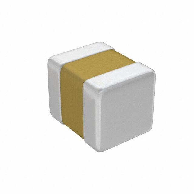


 工商网监
湘ICP备2023018690号
工商网监
湘ICP备2023018690号
