74AVCH1T45
SINGLE BIT DUAL POWER SUPPLY TRANSLATING
TRANSCEIVER WITH 3 STATE OUTPUTS
Description
Pin Assignments
NEW PRODUCT
The 74AVCH1T45 is a single bit, dual supply transceiver with 3-state
outputs suitable for transmitting a single logic bit across different
voltage domains. The 74AVCH1T45 is a variant of the 74AVC1T45
that includes a bus hold feature at each input. The A input/output pin
is designed to track VCCA while the B input/output tracks VCCB. This
(Top View )
Vcc(A) 1
GND 2
arrangement allows for universal low-voltage translation between any
voltages from 1.2V to 3.6V. The Direction pin (DIR) controls the
direction of the transceiver and in a logic voltage related to VCCA.
(Top View )
Vcc(A) 1
GND 2
A
(Bottom View)
A 3
GND 2
Vcc(A) 1
4B
5 DIR
3
6
Vcc(B)
5 DIR
4 B
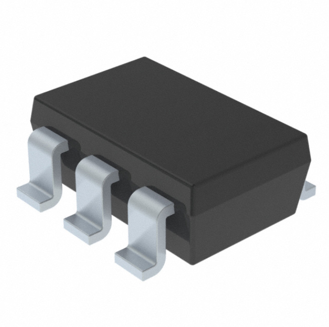
X1-DFN1010-6
X2-DFN0910-6
X2-DFN1410-6
6 Vcc(B)
X2-DFN1409-6
Chip Scale
Alternative
The bus hold feature maintains the previous logic level therefore a
valid logic level is always present eliminating the need for additional
resistors for an unused or disconnected inputs.
Applications
Features
Wide Supply Voltage Range:
VCC(A): from 1.2V to 3.6V
VCC(B): from 1.2V to 3.6V
± 12mA Output Drive at 3.3V
High Noise Immunity - (100mV hysteresis typical)
IOFF Supports Partial-Power-Down Mode Operation
IOFF controlled by either VCC being at 0V
Inputs accept up to 4.6V
ESD Protection Exceeds JESD 22
200-V Machine Model (A115)
2000-V Human Body Model (A114)
1000 V Charged Device Model ( C101)
Latch-Up Exceeds 100mA per JESD 78, Class I
X2-DFN1409-6 package designed as a direct replacement for
chip scale packaging.
Totally Lead-Free & Fully RoHS Compliant (Notes 1 & 2)
Halogen and Antimony Free. “Green” Device (Note 3)
Notes:
4 B
SOT26
SOT363
The 3-state feature occurs when either of the power supply voltages
are zero. This is also an Ioff feature and allows for the output to
remain in a high impedance state with both power supplies at 0V
preventing damaging backflow currents and providing power down
electrical isolation up to 3.6 V as not to interfere with any logic activity
on pin A or B.
5 DIR
A 3
When a high logic level is applied to DIR the A pin becomes an input
and the B pin becomes the output. Conversely the roles of A and B
are reversed when DIR is asserted low.
6 Vcc(B)
Voltage Level Translation:
Well suited to join logic types operating at different voltages
Power Down Signal Isolation:
If either voltage domain is turned off the signal is isolated and
there is no loading on signal lines
Wide array of products such as:
Cell Phones, Tablets, E-Readers
PCs, Notebooks, Netbooks, Ultrabooks
Networking, Routers, Gateways
Computer Peripherals, Hard Drives, CD/DVD ROMs
TVs, DVDs, DVRs, Set Top Boxes
Personal Navigation / GPS
MP3 players, Cameras, Video Recorders
1. No purposely added lead. Fully EU Directive 2002/95/EC (RoHS) & 2011/65/EU (RoHS 2) compliant.
2. See http://www.diodes.com/quality/lead_free.html for more information about Diodes Incorporated’s definitions of Halogen- and Antimony-free, "Green"
and Lead-free.
3. Halogen- and Antimony-free "Green” products are defined as those which contain
很抱歉,暂时无法提供与“74AVCH1T45W6-7”相匹配的价格&库存,您可以联系我们找货
免费人工找货- 国内价格
- 1+0.70512
- 10+0.65088
- 30+0.64003
- 100+0.60749
- 国内价格 香港价格
- 1+3.920661+0.47516
- 10+3.1842410+0.38592
- 25+2.9087625+0.35253
- 100+2.16622100+0.26254
- 250+1.96282250+0.23789
- 500+1.62430500+0.19686
- 1000+1.218301000+0.14765


 工商网监
湘ICP备2023018690号
工商网监
湘ICP备2023018690号
