BCR420UW6Q / BCR421UW6Q
LINEAR LED CONSTANT CURRENT REGULATOR IN SOT26
Description
Features
These linear LED drivers are designed to meet the stringent
requirements of automotive applications.
The BCR420UW6Q and BCR421UW6Q monolithically integrate
transistors, diodes, and resistors to function as a Constant Current
Regulator (CCR) for linear LED driving. The device regulates with a
preset 10mA nominal that can be adjusted with an external resistor up
to 350mA. It is designed for driving LEDs in strings and will reduce
current at increasing temperatures to self-protect. Operating as a
series linear CCR for LED string current control, the device can be
used in multiple applications, as long as the maximum supply voltage
to the device is < 40V.
With the low-side control, the BCR421UW6Q has an Enable (EN) pin
which can be pulse-width modulated (PWM) up to 25 kHz by a microcontroller for LED dimming.
LED Constant Current Regulator using NPN Emitter-Follower with
Emitter Resistor to Current Limit
IOUT – 10mA ± 10% Constant Current (Preset)
IOUT up to 350mA Adjustable with an External Resistor
(BCR421UW6Q)
VOUT – 40V Supply Voltage
PD up to 1W in SOT26
Low-Side Control Enabling PWM Input < 25kHz (BCR421UW6Q)
Negative Temperature Coefficient (NTC) Reduces IOUT with
With no need for additional external components, this CCR is fully
integrated into the SOT26 package, minimizing PCB area and
component count.
Increasing Temperature
Parallel Devices to Increase Regulated Current
Totally Lead-Free & Fully RoHS Compliant (Notes 1 & 2)
Halogen and Antimony Free. “Green” Device (Note 3)
The BCR420UW6Q and BCR420UW6Q are suitable for
automotive applications requiring specific change control;
these parts are AEC-Q100 qualified, PPAP capable, and
manufactured in IATF16949 certified facilities.
https://www.diodes.com/quality/product-definitions/
Applications
Mechanical Data
Constant Current Regulation (CCR) in:
Automotive interior lighting
Mood and decorative lighting
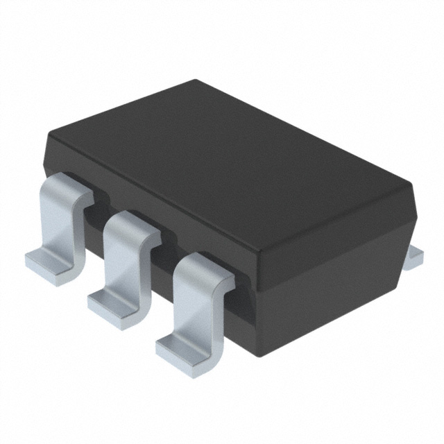
SOT26
EN
Package: SOT26
Package Material: Molded Plastic. “Green” Molding Compound.
UL Flammability Rating 94V-0
Moisture Sensitivity: Level 1 per J-STD-020
Terminals: Finish - Matte Tin Plated Leads.
Solderable per MIL-STD-202, Method 208
Weight: 0.018 grams (Approximate)
OUT
BCR420U
BCR421U
REXT
(Optional)
EN
Pin Name
Pin Function
REXT
OUT
OUT
OUT
EN
OUT
GND
REXT
Regulated Output Current
Enable for Biasing
Transistor
External Resistor for
Adjusting Output Current
GND
Power Ground
GND
Top View
Internal Device
Schematic
Top View
Pin-Out
Ordering Information (Note 4)
Product
BCR420UW6Q-7
BCR421UW6Q-7
Notes:
Compliance
Automotive
Automotive
Marking
420
421
Reel Size (inches)
7
7
Tape Width (mm)
8
8
Quantity per Reel
3,000
3,000
1. No purposely added lead. Fully EU Directive 2002/95/EC (RoHS), 2011/65/EU (RoHS 2) & 2015/863/EU (RoHS 3) compliant.
2. See https://www.diodes.com/quality/lead-free/ for more information about Diodes Incorporated’s definitions of Halogen- and Antimony-free, "Green" and
Lead-free.
3. Halogen- and Antimony-free "Green” products are defined as those which contain 2.0V; VEN = 24V
VOUT > 2.0V; VEN = 3.3V
VOUT > 2.0V; VEN = 24V
VOUT > 2.0V; VEN = 3.3V
January 2022
© Diodes Incorporated
�BCR420UW6Q / BCR421UW6Q
1.4
800
1.2
700
50mm * 50mm
1oz Cu
1.0
Rth(JA) ( C/W)
0.8
o
Max Power Dissipation (W)
Typical Thermal Characteristics BCR420UW6Q/BCR421UW6Q (@TA = +25°C, unless otherwise specified.)
0.6
0.4
25mm * 25mm
1oz Cu
0.2
0.0
600
500
400
300
200
100
0
0
50
100
100
150
1000
2
o
Copper Area (mm )
Temperature ( C)
Rth(JA) VS Cu Area
Derating Curve
75
50
Maximum Power (W)
o
T amb=25 C
100
o
Thermal Resistance ( C/W)
125
50mm * 50mm
1oz Cu
D=0.5
Single Pulse
D=0.2
D=0.05
25
D=0.1
0
100μµ
1m
10m 100m
1
10
100
o
Single Pulse
50mm * 50mm
1oz Cu
1
100μ
µ
1k
T amb=25 C
10
1m
Pulse Width (s)
10m 100m
1
10
100
1k
Pulse Width (s)
Transient Thermal Impedance
Pulse Power Dissipation
100
o
Maximum Power (W)
125
o
Thermal Resistance ( C/W)
150
T amb=25 C
25mm * 25mm
1oz Cu
D=0.5
75
50
D=0.2
Single Pulse
D=0.05
25
D=0.1
0
100μµ 1m
10m 100m
1
10
100
1k
1
100μµ
1m
10m 100m
1
10
100
1k
Pulse Width (s)
Transient Thermal Impedance
Document number: DS38302 Rev. 5 - 2
T amb=25 C
25mm * 25mm
1oz Cu
Pulse Width (s)
BCR420UW6Q / BCR421UW6Q
Single Pulse
o
10
Pulse Power Dissipation
4 of 13
www.diodes.com
January 2022
© Diodes Incorporated
�BCR420UW6Q / BCR421UW6Q
Typical Electrical Characteristics BCR421U (@ TA = +25°C, unless otherwise specified.)
0.20
0.20
VEN=3.3V
REXT=6.2
REXT=8.2
VOUT=5.4V
0.15
REXT=10
IOUT (A)
IOUT (A)
0.16
0.12
0.08
REXT= 30
REXT=15
VOUT=1.4V
0.10
0.05
0.04
VEN=3.3V
REXT=open
0.000
1
2
3
4
5
6
7
8
9 10 11 12
0.00
1
10
100
REXT ()
VOUT (V)
REXT () vs IOUT
VOUT vs IOUT
0.18
o
-40 C
0.06
0.16
o
-40 C
0.05
IOUT (A)
IOUT (A)
0.14
0.12
o
25 C
0.10
o
85 C
VEN=3.3V
0.08
0.06
0.04
o
25 C
o
85 C
VEN=3.3V
0.03
REXT=20
REXT=6.2
0
2
4
6
8
10
0.02
0
12
VOUT (V)
2
4
6
VOUT (V)
8
10
12
VOUT vs IOUT
VOUT vs IOUT
0.15
0.02
REXT=8.2
VOUT=2V
REXT=6.2
REXT=10
o
IOUT (A)
IOUT (A)
-40 C
0.01
o
85 C
0.00
0
2
4
6
REXT= 60
0.05
REXT= open
REXT=open
8
10
12
0.00
0
1
2
3
VOUT (V)
VEN (V)
VOUT vs IOUT
VEN vs IOUT
BCR420UW6Q / BCR421UW6Q
Document number: DS38302 Rev. 5 - 2
REXT=30
VEN=3.3V
o
25 C
0.10
5 of 13
www.diodes.com
4
5
January 2022
© Diodes Incorporated
�BCR420UW6Q / BCR421UW6Q
Typical Electrical Characteristics BCR421U (@ TA = +25°C, unless otherwise specified.) (continued)
0.015
3.0m
o
-40 C
IOUT=0A
o
o
85 C
REXT=open
2.0m
IOUT (A)
IEN (mA)
2.5m
1.5m
1.0m
o
25 C
o
-40 C
25 C
0.010
o
85 C
0.005
VOUT=2V
500.0µ
500.0μ
REXT=open
0.0
0
1
2
3
4
0.000
0
5
1
VEN (V)
2
3
4
5
VEN (V)
VENvs IOUT
VENvs IEN
0.06
0.20
o
-40 C
o
-40 C
0.05
IOUT (A)
IOUT (A)
0.15
0.04
o
o
85 C
25 C
0.03
o
25 C
o
0.10
85 C
0.02
0.01
0.00
VOUT=2V
0.05
VOUT=2V
REXT=6.2
REXT= 20
0
1
2
3
4
5
0.00
0
VENvs IOUT
BCR420UW6Q / BCR421UW6Q
Document number: DS38302 Rev. 5 - 2
1
2
3
4
5
VEN (V)
VEN (V)
VEN vs IOUT
6 of 13
www.diodes.com
January 2022
© Diodes Incorporated
�BCR420UW6Q / BCR421UW6Q
Typical Electrical Characteristics BCR420UW6Q (@TA = +25°C, unless otherwise specified.)
0.20
0.20
REXT=6.2
0.16
REXT=8.2
VOUT = 5.4V
0.15
REXT=10
IOUT (A)
IOUT (A)
VEN=24V
0.12
0.08
REXT=15
REXT= 30
0.04
0.10
0.05
VEN=24V
REXT=open
0.00
0
1
2
3
4
5
6
7
VOUT (V)
8
VOUT=1.4V
0.00
1
9 10 11 12
10
100
REXT ()
REXT ()vs IOUT
VOUT vs IOUT
0.18
o
-40 C
0.06
0.16
o
-40 C
IOUT (A)
IOUT (A)
0.14
0.12
o
25 C
0.10
0.04
o
25 C
85 C
VEN=24V
VEN=24V
0.03
REXT=20
REXT=6.2
0
2
4
6
8
10
0.02
0
12
VOUT (V)
2
4
6
VOUT (V)
8
10
12
VOUT vs IOUT
VOUT vs IOUT
0.15
0.02
VOUT=2V
IOUT (A)
IOUT (A)
0.01
o
o
85 C
4
6
0.10
REXT=open
0.05
REXT=open
8
10
12
0.00
0
5
10
15
20
25
30
VEN (V)
VOUT vs IOUT
Document number: DS38302 Rev. 5 - 2
REXT=30
REXT=60
VOUT (V)
BCR420UW6Q / BCR421UW6Q
Rext=10
VEN=24V
25 C
2
REXT=8
REXT=20
o
-40 C
0.00
0
o
85 C
o
0.08
0.06
0.05
VEN vs IOUT
7 of 13
www.diodes.com
January 2022
© Diodes Incorporated
�BCR420UW6Q / BCR421UW6Q
Typical Electrical Characteristics BCR420UW6Q (@TA = +25°C, unless otherwise specified.) (continued)
0.015
3.0m
o
-40 C
2.5m
IOUT=0A
o
IOUT (A)
1.5m
1.0m
o
25 C
25 C
0.010
IEN (mA)
2.0m
o
85 C
REXT=open
o
85 C
0.005
o
-40 C
VOUT=2V
500.0μ
500.0µ
REXT=open
0.000
0.0
0
5
10
15
20
25
30
VEN (V)
35
0
40
5
10
VENvs IEN
15
VEN (V)
20
25
30
VENvs IOUT
0.06
0.20
o
-40 C
o
-40 C
0.05
0.15
o
85 C
o
25 C
o
25 C
IOUT (A)
IOUT (A)
0.04
0.03
0.10
0.02
VOUT=2V
0.01
o
85 C
VOUT=2V
0.05
REXT=6.2
REXT=20
0.00
0.00
0
5
10
15
20
VEN (V)
25
30
Document number: DS38302 Rev. 5 - 2
5
10
15
VEN (V)
20
25
30
VENvs IOUT
VENvs IOUT
BCR420UW6Q / BCR421UW6Q
0
8 of 13
www.diodes.com
January 2022
© Diodes Incorporated
�BCR420UW6Q / BCR421UW6Q
Application Information
The BCR420UW6Q and BCR421UW6Q are designed for driving low
current LEDs with typical LED currents of 10mA to 350mA. They
provide a cost-effective way for driving low current LEDs compared with
more complex switching regulator solutions. Furthermore, they reduce
the PCB board area of the solution as there is no need for external
components like inductors, capacitors, and switching diodes.
Figure 1 shows a typical application circuit diagram for driving an LED
or string of LEDs. The device comes with an internal resistor (RINT) of
typically 95Ω, which in the absence of an external resistor, sets an LED
current of 10mA (typical) from a VEN = 3.3V and VOUT = 1.4V for
BCR421; or VEN = 24V and VOUT = 1.4V for BCR420. LED current can
be increased to a desired value by choosing an appropriate external
resistor, REXT.
The REXT Vs IOUT graphs should be used to select the appropriate
resistor. Choosing a low tolerance REXT will improve the overall
accuracy of the current sense formed by the parallel connection of RINT
and REXT.
Figure 1 Typical Application Circuit for
Linear Mode Current Sink LED Driver
Two or more BCR420UW6Q/BCR421UW6Q can be connected in
parallel to construct higher current LED strings as shown in Figure 2.
Consideration of the expected linear mode power dissipation must be
factored
into
the
design,
with
respect
to
the
BCR420UW6Q/BCR421UW6Q’s thermal resistance. The maximum
voltage across the device can be calculated by taking the maximum
supply voltage and subtracting the voltage across the LED string.
VOUT = VS – VLED
PD = (VOUT × ILED) + (VEN × IEN)
As the output current of BCR420UW6Q/BCR421UW6Q increases, it is
necessary to provide appropriate thermal relief to the device. The power
dissipation supported by the device is dependent upon the PCB board
material, the copper area and the ambient temperature. The maximum
dissipation the device can handle is given by:
Figure 2 Application Circuit for Increasing LED Current
PD = (TJ(MAX) - TA) / RθJA
Refer to the thermal characteristic graphs on Page 4 for selecting the
appropriate PCB copper area.
BCR420UW6Q / BCR421UW6Q
Document number: DS38302 Rev. 5 - 2
9 of 13
www.diodes.com
January 2022
© Diodes Incorporated
�BCR420UW6Q / BCR421UW6Q
Application Information (continued)
PWM dimming can be achieved by driving the EN pin. Dimming is achieved by turning the LEDs ON and OFF for a portion of a single cycle. The
PWM signal can be provided by a micro-controller or analog circuitry; typical circuit is shown in Figure 3. Figure 4 shows a typical response of LED
current vs. PWM duty cycle on the EN pin; PWM up to 25kHz with duty cycle of 0.5% (dimming range 200:1). This is above the audio-bandminimizing audible power-supply noise.
Figure 3 Application Circuits for LED Driver with PWM Dimming Functionality using BCR421UW6Q
Figure 4 Typical LED Current Response vs. PWM Duty Cycle for
25kHz PWM Frequency (Dimming Range 200:1)
BCR420UW6Q / BCR421UW6Q
Document number: DS38302 Rev. 5 - 2
10 of 13
www.diodes.com
January 2022
© Diodes Incorporated
�BCR420UW6Q / BCR421UW6Q
Application Information (continued)
To remove the potential of incorrect connection of the power supply
damaging the lamp’s LEDs, many systems use some form of
reverse polarity protection.
One solution for reverse input polarity protection is to simply use a
diode with a low VF in line with the driver/LED combination. The low
VF increases the available voltage to the LED stack and dissipates
less power. A circuit example is presented in Figure 5, which
protects the light engine, although it will not function until the
problem is diagnosed and corrected. An SDM10U45LP (0.1A/45V)
is shown, providing exceptionally low VF for its package size of 1mm
x 0.6mm. Other reverse voltage ratings are available from Diodes
Incorporated’s website such as the SBR02U100LP (0.2A/100V) or
SBR0220LP (0.2A/20V).
While automotive applications commonly use this method for
reverse battery protection, an alternative approach shown in Figure
6, provides reverse polarity protection and corrects the reversed
polarity, allowing the light engine to function.
The BAS40BRW incorporates four low VF Schottky diodes in a
single package, reducing the power dissipated and maximizes the
voltage across the LED stack.
Figure 5 Application Circuit for LED Driver
with Reverse Polarity Protection
Figure 6 Application Circuit for LED Driver with
Assured Operation Regardless Of Polarity
BCR420UW6Q / BCR421UW6Q
Document number: DS38302 Rev. 5 - 2
Figure 7 shows an example configuration for 350mA operation using
BCR421UW6Q. In such higher current configurations, adequate
enable current is provided by increasing the enable voltage.
Figure 7 Example for 350mA Operation using BCR421UW6Q
11 of 13
www.diodes.com
January 2022
© Diodes Incorporated
�BCR420UW6Q / BCR421UW6Q
Package Outline Dimensions
Please see http://www.diodes.com/package-outlines.html for the latest version.
SOT26
D
E1
SOT26
Dim Min Max
Typ
A1 0.013 0.10
0.05
A2 1.00 1.30
1.10
A3 0.70 0.80
0.75
b
0.35 0.50
0.38
c
0.10 0.20
0.15
D
2.90 3.10
3.00
e
0.95
e1
1.90
E
2.70 3.00
2.80
E1 1.50 1.70
1.60
L
0.35 0.55
0.40
a
8°
a1
7°
All Dimensions in mm
E
b
a1
e1
A2
A3
A1
Seating Plane
e
L
c
a
Suggested Pad Layout
Please see http://www.diodes.com/package-outlines.html for the latest version.
SOT26
C1
Y1
G
C
Y
Dimensions Value (in mm)
C
2.40
C1
0.95
G
1.60
X
0.55
Y
0.80
Y1
3.20
X
BCR420UW6Q / BCR421UW6Q
Document number: DS38302 Rev. 5 - 2
12 of 13
www.diodes.com
January 2022
© Diodes Incorporated
�BCR420UW6Q / BCR421UW6Q
IMPORTANT NOTICE
1.
DIODES INCORPORATED AND ITS SUBSIDIARIES (“DIODES”) MAKE NO WARRANTY OF ANY KIND, EXPRESS OR IMPLIED,
WITH REGARDS TO ANY INFORMATION CONTAINED IN THIS DOCUMENT, INCLUDING, BUT NOT LIMITED TO, THE IMPLIED
WARRANTIES OF MERCHANTABILITY, FITNESS FOR A PARTICULAR PURPOSE OR NON-INFRINGEMENT OF THIRD PARTY
INTELLECTUAL PROPERTY RIGHTS (AND THEIR EQUIVALENTS UNDER THE LAWS OF ANY JURISDICTION).
2.
The Information contained herein is for informational purpose only and is provided only to illustrate the operation of Diodes products
described herein and application examples. Diodes does not assume any liability arising out of the application or use of this document or any
product described herein. This document is intended for skilled and technically trained engineering customers and users who design with Diodes
products. Diodes products may be used to facilitate safety-related applications; however, in all instances customers and users are responsible for
(a) selecting the appropriate Diodes products for their applications, (b) evaluating the suitability of the Diodes products for their intended
applications, (c) ensuring their applications, which incorporate Diodes products, comply the applicable legal and regulatory requirements as well
as safety and functional-safety related standards, and (d) ensuring they design with appropriate safeguards (including testing, validation, quality
control techniques, redundancy, malfunction prevention, and appropriate treatment for aging degradation) to minimize the risks associated with
their applications.
3.
Diodes assumes no liability for any application-related information, support, assistance or feedback that may be provided by Diodes
from time to time. Any customer or user of this document or products described herein will assume all risks and liabilities associated with such
use, and will hold Diodes and all companies whose products are represented herein or on Diodes’ websites, harmless against all damages and
liabilities.
4.
Products described herein may be covered by one or more United States, international or foreign patents and pending patent
applications. Product names and markings noted herein may also be covered by one or more United States, international or foreign trademarks
and trademark applications. Diodes does not convey any license under any of its intellectual property rights or the rights of any third parties
(including third parties whose products and services may be described in this document or on Diodes’ website) under this document.
5.
Diodes
products
are
provided
subject
to
Diodes’
Standard
Terms
and
Conditions
of
Sale
(https://www.diodes.com/about/company/terms-and-conditions/terms-and-conditions-of-sales/) or other applicable terms. This document does not
alter or expand the applicable warranties provided by Diodes. Diodes does not warrant or accept any liability whatsoever in respect of any
products purchased through unauthorized sales channel.
6.
Diodes products and technology may not be used for or incorporated into any products or systems whose manufacture, use or sale is
prohibited under any applicable laws and regulations. Should customers or users use Diodes products in contravention of any applicable laws or
regulations, or for any unintended or unauthorized application, customers and users will (a) be solely responsible for any damages, losses or
penalties arising in connection therewith or as a result thereof, and (b) indemnify and hold Diodes and its representatives and agents harmless
against any and all claims, damages, expenses, and attorney fees arising out of, directly or indirectly, any claim relating to any noncompliance with
the applicable laws and regulations, as well as any unintended or unauthorized application.
7.
While efforts have been made to ensure the information contained in this document is accurate, complete and current, it may contain
technical inaccuracies, omissions and typographical errors. Diodes does not warrant that information contained in this document is error-free and
Diodes is under no obligation to update or otherwise correct this information. Notwithstanding the foregoing, Diodes reserves the right to make
modifications, enhancements, improvements, corrections or other changes without further notice to this document and any product described
herein. This document is written in English but may be translated into multiple languages for reference. Only the English version of this document
is the final and determinative format released by Diodes.
8.
Any unauthorized copying, modification, distribution, transmission, display or other use of this document (or any portion hereof) is
prohibited. Diodes assumes no responsibility for any losses incurred by the customers or users or any third parties arising from any such
unauthorized use.
Copyright © 2022 Diodes Incorporated
www.diodes.com
BCR420UW6Q / BCR421UW6Q
Document number: DS38302 Rev. 5 - 2
13 of 13
www.diodes.com
January 2022
© Diodes Incorporated
�


 工商网监
湘ICP备2023018690号
工商网监
湘ICP备2023018690号
