A Product Line of
Diodes Incorporated
PAM2861
1A LED DRIVER WITH INTERNAL SWITCH
Description
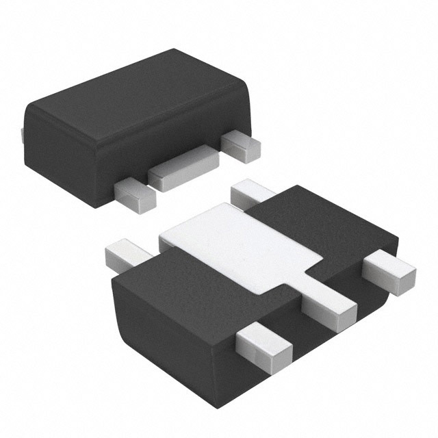
Pin Assignments
The PAM2861 is a continuous mode inductive step-down converter,
Top View
TSOT25
designed for driving single or multiple series connected LEDs
efficiently from a voltage source higher than the LED voltage. The
device operates from an input supply between 6V and 40V and
provides an externally adjustable output current of up to 1A.
Depending upon supply voltage and external components, this can
provide up to 30 watts of output power.
The PAM2861 includes the output switch and a high-side output
current sensing circuit, which uses an external resistor to set the
nominal average output current.
Output current can be adjusted below the set value, by applying an
external control signal to the VSET pin.
The VSET pin will accept either a DC voltage or a PWM waveform.
The soft-start time can be increased using an external capacitor from
the VSET pin to ground. Applying a voltage of 0.2V or lower to the
VSET pin turns the output off and switches the device into a low
current standby state.
Features
Applications
Simple Low Parts Count
Internal 40V NDMOS Switch
1A Output Current
Single Pin On/Off and Brightness Control Using DC Voltage or
PWM
Soft-Start
High Efficiency (up to 97%)
Wide Input Voltage Range: 6V to 40V
Output Shutdown
Open LED Protection
Short LED Protection
Up to 1MHz Switching Frequency
Inherent Open-Circuit LED Protection
Typical 5% Output Current Accuracy
Pb-free TSOT25 and SOT89-5 Packages
PAM2861
Document number: DSxxxxx Rev. 1 - 1
Low voltage halogen replacement LEDs
Low voltage industrial lighting
LED back-side lighting
Illuminated signs
1 of 12
www.diodes.com
July 2013
© Diodes Incorporated
�A Product Line of
Diodes Incorporated
PAM2861
Typical Applications Circuit
Pin Descriptions
Pin
Number
1
2
Pin
Name
LX
GND
3
VSET
4
ISENSE
5
VIN
Function
Drain of NDMOS switch.
Ground (0V)
• Multi-function On/Off and brightness control pin:
• Leave floating for normal operation.
• Drive to voltage below 0.2V to turn off output current
• Drive with DC voltage (0.3V < VSET< 2.5V) to adjust output current from 12% to 100% of IOUTnom
• Drive with PWM signal from open-collector or open-drain transistor, to adjust output current. Adjustment range
1% to 100% of IOUTnom for f < 500Hz
• Connect a capacitor from this pin to ground to increase soft-start time.
(Default soft-start time = 0.1ms. Additional soft-start time is approx.1.5ms/1nF)
Connect resistor RS from this pin to VIN to define nominal average output current
IOUTnom = 0.1/Rs
Input voltage (6V to 40V). Decouple to ground with 10μF or higher X7R ceramic capacitor close to device.
PAM2861
Document number: DSxxxxx Rev. 1 - 1
2 of 12
www.diodes.com
July 2013
© Diodes Incorporated
�A Product Line of
Diodes Incorporated
PAM2861
Functional Block Diagram
Absolute Maximum Ratings (@TA = +25°C, unless otherwise specified.)
These are stress ratings only and functional operation is not implied. Exposure to absolute maximum ratings for prolonged time periods may
affect device reliability. All voltages are with respect to ground.
Parameter
Input Voltage Range
Rating
-0.3 to +40
Unit
LX, ISENSE Pin Voltage
VSET Pin Voltage
Maximum Junction Temperature
Storage Temperature
Soldering Temperature
-0.3 to +40
V
-0.3 to +6.0
170
-65 to +170
300, 5sec
°C
Recommended Operating Conditions (@TA = +25°C, unless otherwise specified.)
Parameter
Input Voltage Range
Ambient Temperature Range
Junction Temperature Range
PAM2861
Document number: DSxxxxx Rev. 1 - 1
Rating
6 to 40
-40 to +85
-40 to +150
3 of 12
www.diodes.com
Unit
V
°C
July 2013
© Diodes Incorporated
�A Product Line of
Diodes Incorporated
PAM2861
Thermal Information
Parameter
Thermal Resistance (Junction to Ambient)
Thermal Resistance (Junction to Case)
Package
TSOT25
SOT89-5
TSOT25
SOT89-5
Symbol
θJA
θJC
Max
250
160
130
45
Unit
°C/W
Electrical Characteristics (@TA = +25°C, VIN = 16V, unless otherwise specified.)
Parameter
Input Voltage
Symbol
Test Conditions
Min
Typ
6
VIN
40
333
RS = 0.3Ω
Output Current
ILED
RS = 0.1Ω
1
Shutdown Current
ISD
VSET Pin Grouded
20
Quiescent Current without Switching
IQ
VSET Pin Floating, VIN = 16V
0.6
VSENSE
Measured on ISENSE Pin with
Respect to VIN
Mean Current Sense Threshold Voltage
Sense Threshold Hysteresis
Max
95
100
ISENSE Pin Input Current
ISENSE
VSENSE = VIN -0.1
VSET Range on VSET Pin
VEN
For DC Dimming
A
40
µA
mA
105
mV
%
8
0.3
V
mA
±13
VSENSE_HYS
Units
µA
2.5
V
DC Voltage on VSET Pin to Enable
VEN(ON)
VEN Rising
0.25
DC Voltage on VSET Pin to Disable
VEN(OFF)
VEN Falling
0.2
V
@ILX = 100mA
0.3
Ω
LX Switch On Resistance
LX Switch Leakage Current
RLX
V
5
ILX(LEAK)
µA
Soft Start Time
TSS
VIN = 16V, CEN = 1nF
1.5
ms
Operating Frequency
FLX
VI = 16V, VO = 9.6V (3 LEDs)
L = 47µF, ΔI = 0.25A (ILED = 1A)
233
kHz
For 4% Accuracy
500
Recommended Minimum Switch ON Time
TON_REC
Recommended Maximum Switch Frequency
FLX(MAX)
Max Duty Circle
Recommended Duty Cycle Range
Internal Comparator Propagation Delay
Over Temperature Protection
Temp Protection Hysteresis
Current Limit
Note:
Ns
1.0
MHz
75
%
98
25
DLX
%
TPD (Note 1)
45
ns
TOTP
150
°C
40
°C
TOTP_HYS
IXL(MAX)
Peak Inductor Current
1.5
A
1. Parameters are not tested at production, but guaranteed by design. VSENSE: level A: 95mV to 100mV; level B: 100mV to 105mV.
PAM2861
Document number: DSxxxxx Rev. 1 - 1
4 of 12
www.diodes.com
July 2013
© Diodes Incorporated
�A Product Line of
Diodes Incorporated
PAM2861
Typical Performance Characteristics (@TA = +25°C, VIN = 16V, unless otherwise specified.)
PAM2861
Document number: DSxxxxx Rev. 1 - 1
5 of 12
www.diodes.com
July 2013
© Diodes Incorporated
�A Product Line of
Diodes Incorporated
PAM2861
Typical Performance Characteristics (cont.) (@TA = +25°C, VIN = 16V, unless otherwise specified.)
PAM2861
Document number: DSxxxxx Rev. 1 - 1
6 of 12
www.diodes.com
July 2013
© Diodes Incorporated
�A Product Line of
Diodes Incorporated
PAM2861
Typical Performance Characteristics (cont.) (@TA = +25°C, CIN = 10µF, CO = 10µF, L = 4.7µH, unless otherwise specified.)
PAM2861
Document number: DSxxxxx Rev. 1 - 1
7 of 12
www.diodes.com
July 2013
© Diodes Incorporated
�A Product Line of
Diodes Incorporated
PAM2861
Application Information
Setting Nominal Average Output Current with External Resistor RS
The nominal average output current in the LED(s) is determined by the value of the external current sense resistor (RS) connected between VIN
and ISENSE and is given by:
IOUT(NOM)
0 .1
RS
The table below gives values of nominal average output current for several preferred values of current setting resistor (RS) in the typical
application circuit shown on page 1.
Nominal Average Output
Current (mA)
1000
760
667
333
RS (Ω)
0.1
0.13
0.15
0.3
The above values assume that the VSET pin is floating and at a nominal voltage of VREF (1.25V). Note that RS = 0.1Ω is the minimum allowed
value of sense resistor under these conditions to maintain switch current below the specified maximum value. It is possible to use different
values of RS if the VSET pin is driven from an external voltage.
Capacitor Selection
A low ESR capacitor should be used for input decoupling, as the ESR of this capacitor appears in series with the supply source impedance and
lowers overall efficiency. This capacitor has to supply the relatively high peak current to the coil and smooth the current ripple on the input
supply.
A minimum value of 4.7µF is acceptable if the input source is close to the device, but higher values will improve performance at lower input
voltages, especially when the source impedance is high. The input capacitor should be placed as close as possible to the IC.
For maximum stability over temperature and voltage, capacitors with X7R, X5R, or better dielectric are recommended. Capacitors with
Y5Vdielectric are not suitable for decoupling in this application and should NOT be used.
Inductor Selection
Recommended inductor values for the PAM2861 are in the range 33µH to 100µH. Higher values of inductance are recommended at higher
supply voltages in order to minimize errors due to switching delays, which in increased ripple and lower efficiency. Higher values of inductance
also result in a smaller change in output current over the supply voltage range. The inductor should be mounted as close to the device as
possilbe with low resistance connections to the LX and VIN pins. The chosen coil should have a saturation current higher than the peak output
current and a continuous current rating above the required mean output current.
The inductor value should be chosen to maintain operating duty cycle and switch ‘on’/’off’ times within the specified limits over the supply voltage
and load current range. The following equations can be used as a guide.
LX Switch ‘On’ time
TON
LI
VIN VLED ILED (RS RL RLX )
Lx Switch ‘Off’ time
TOFF
LI
VLED VD ILED (RS RL )
Where: L is the coil inductance; RL is the coil resistance; RS is the current sense resistance ILED is the required LED current; ΔI is the coil peakpeak ripple current (Internally set to 0.25 x ILED); VIN is the supply voltage; VLED is the total LED forward voltage; RLX is the switch resistance
(0.3Ω nominal); VD is the diode forward voltage at the required load current
PAM2861
Document number: DSxxxxx Rev. 1 - 1
8 of 12
www.diodes.com
July 2013
© Diodes Incorporated
�A Product Line of
Diodes Incorporated
PAM2861
Application Information (cont.)
Diode Selection
For maximum efficiency and performance, the rectifier (D1) should be a fast low capacitance Schottky diode with low reverse leakage at the
maximum operating voltage and temperature. They also provide better efficiency than silicon diodes, due to a combination of lower forward
voltage and reduced recovery time.
It is important to select parts with a peak current rating above the peak coil current and a continuous current rating higher than the maximum
output load current. It is very important to consider the reverse leakage of the diode when operating above +85°C. Excess leakage will increase
the power dissipation in the device and if close to the load may create a thermal runaway condition.
The higher forward voltage and overshoot due to reverse recovery time in silicon diodes will increase the peak voltage on the LX output. If a
silicon diode is used, care should be taken to ensure that the total voltage appearing on the LX pin including supply ripple, does not exceed the
specified maximum value.
Ordering Information
Part Number
PAM2861ABR
PAM2861CBR
Part Marking
EQXYW
P2861
XXXYW
Package Type
TSOT25
Standard Package
3000 Units/ Tape&Reel
SOT89-5
1000 Units/ Tape&Reel
Marking Information
Top View
TSOT25
PAM2861
Document number: DSxxxxx Rev. 1 - 1
9 of 12
www.diodes.com
July 2013
© Diodes Incorporated
�A Product Line of
Diodes Incorporated
PAM2861
Package Outline Dimensions (All dimensions in mm.)
TSOT25
PAM2861
Document number: DSxxxxx Rev. 1 - 1
10 of 12
www.diodes.com
July 2013
© Diodes Incorporated
�A Product Line of
Diodes Incorporated
PAM2861
Package Outline Dimensions (cont.) (All dimensions in mm.)
SOT89-5
PAM2861
Document number: DSxxxxx Rev. 1 - 1
11 of 12
www.diodes.com
July 2013
© Diodes Incorporated
�A Product Line of
Diodes Incorporated
PAM2861
IMPORTANT NOTICE
DIODES INCORPORATED MAKES NO WARRANTY OF ANY KIND, EXPRESS OR IMPLIED, WITH REGARDS TO THIS DOCUMENT,
INCLUDING, BUT NOT LIMITED TO, THE IMPLIED WARRANTIES OF MERCHANTABILITY AND FITNESS FOR A PARTICULAR PURPOSE
(AND THEIR EQUIVALENTS UNDER THE LAWS OF ANY JURISDICTION).
Diodes Incorporated and its subsidiaries reserve the right to make modifications, enhancements, improvements, corrections or other changes
without further notice to this document and any product described herein. Diodes Incorporated does not assume any liability arising out of the
application or use of this document or any product described herein; neither does Diodes Incorporated convey any license under its patent or
trademark rights, nor the rights of others. Any Customer or user of this document or products described herein in such applications shall assume
all risks of such use and will agree to hold Diodes Incorporated and all the companies whose products are represented on Diodes Incorporated
website, harmless against all damages.
Diodes Incorporated does not warrant or accept any liability whatsoever in respect of any products purchased through unauthorized sales channel.
Should Customers purchase or use Diodes Incorporated products for any unintended or unauthorized application, Customers shall indemnify and
hold Diodes Incorporated and its representatives harmless against all claims, damages, expenses, and attorney fees arising out of, directly or
indirectly, any claim of personal injury or death associated with such unintended or unauthorized application.
Products described herein may be covered by one or more United States, international or foreign patents pending. Product names and markings
noted herein may also be covered by one or more United States, international or foreign trademarks.
This document is written in English but may be translated into multiple languages for reference. Only the English version of this document is the
final and determinative format released by Diodes Incorporated.
LIFE SUPPORT
Diodes Incorporated products are specifically not authorized for use as critical components in life support devices or systems without the express
written approval of the Chief Executive Officer of Diodes Incorporated. As used herein:
A. Life support devices or systems are devices or systems which:
1. are intended to implant into the body, or
2. support or sustain life and whose failure to perform when properly used in accordance with instructions for use provided in the
labeling can be reasonably expected to result in significant injury to the user.
B. A critical component is any component in a life support device or system whose failure to perform can be reasonably expected to cause the
failure of the life support device or to affect its safety or effectiveness.
Customers represent that they have all necessary expertise in the safety and regulatory ramifications of their life support devices or systems, and
acknowledge and agree that they are solely responsible for all legal, regulatory and safety-related requirements concerning their products and any
use of Diodes Incorporated products in such safety-critical, life support devices or systems, notwithstanding any devices- or systems-related
information or support that may be provided by Diodes Incorporated. Further, Customers must fully indemnify Diodes Incorporated and its
representatives against any damages arising out of the use of Diodes Incorporated products in such safety-critical, life support devices or systems.
Copyright © 2013, Diodes Incorporated
www.diodes.com
PAM2861
Document number: DSxxxxx Rev. 1 - 1
12 of 12
www.diodes.com
July 2013
© Diodes Incorporated
�


 工商网监
湘ICP备2023018690号
工商网监
湘ICP备2023018690号
