PI2EQX6874
6.5Gbps 4-Lane SAS2/SATA3/XAUI ReDriver™with
Equalization,De-emphasis and Flow-through pinout
Features
Description
ÎÎUp to 6.5Gbps SAS2/SATA3/XAUI ReDriver
Pericom Semiconductor’s PI2EQX6874 is a 6.5Gbps low
power, 4 lane (8-channel) SAS2, SATA3, XAUI signal ReDriver.
The device provides programmable equalization, amplification, and de-emphasis by I2C control, to optimize performance over a variety of physical mediums by reducing
Inter-symbol interference.
ÎÎSupporting 8 differential channels or 4 lanes
ÎÎPer channel I2C configuration controls (3.3V Tolerant)
ÎÎAdjustable receiver equalization
ÎÎAdjustable transmitter amplitude and de-emphasis
PI2EQX6874 supports eight 100-Ohm Differential CML data
I/O’s between the Protocol ASIC to a switch fabric, across a backplane, or extends the signals across other distant data pathways
on the user’s platform.
ÎÎ50-Ohm input/output termination
ÎÎMux/Demux feature
ÎÎChannel loop-back
ÎÎOOB fully supported
The integrated equalization circuitry provides flexibility with
signal integrity of the signal before the ReDriver, whereas the
integrated de-emphasis circuitry provides flexibility with signal
integrity of the signal after the ReDriver.
ÎÎSingle supply voltage, 1.2V ± 5%
ÎÎActive Current per channel - 95mA (typical)
ÎÎPower down modes
In addition to providing signal re-conditioning, Pericom’s
PI2EQX6874 also provides power management Stand-by mode
operated by a Power Down pin, or through I2C register. When
input is idle, the device goes into power saving Slumber mode.
àà Slumber current per channel -10mA (typical)
àà Standby current -1mA (typical)
ÎÎIndustrial temperature range: -40°C to 85°C
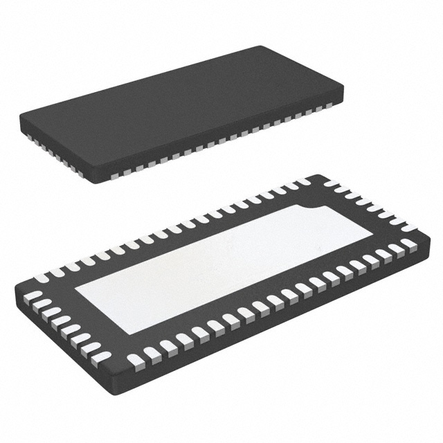
ÎÎPackaging: 56-contact TQFN (5mm x 11mm)
xyRx-
−
xyTx+
+
A
xyTx-
−
B
Equalizer
Output
Controls
Equalizer
Input�level�detect
to�control�logic
+
xyTx+
−
xyTx-
VDD
A0RX+
A0RXB0TX+
B0TX-
+
xyRx+
−
xyRx-
+
Data�Lane�Repeats�4�Times
SELy_x
Sy_x
Dy_x
Mode
Control�Registers
&�Logic
LB#
PRE_x
PD#
SDA
Power
Management
I2C�Control
6
7
A1RX-
8
9
10
43
42
41
40
39
VDD
A2RX+
A2RXB2TX-
11
38
12
13
14
37
36
B2TX+
15
VDD
A3RX+
A3RX-
16
17
18
19
20
B3TX+
B3TX-
35
34
33
32
31
30
29
21 22 23 24 25 26 27 28
All trademarks are property of their respective owners.
A0TX+
A0TXB0RX+
B0RXVDD
A1TX+
A1TXB1RXB1RX+
VDD
A2TX+
A2TXB2RXB2RX+
VDD
A3TX+
A3TXB3RX+
B3RXVDD
Ax
VDD
SIG_B
MODE
NC
SCL
VDD
A1RX+
B1TXB1TX+
−
56 55 54 53 52 51 50 49
1
48
2
47
3
46
4
45
5
44
15-0181
1
A0
A1
LB#
+
A4
xyRx+
Output
Controls
Input�level�detect
to�control�logic
VDD
GND
GND
NC
SCL
+
−
SDA
PD#
SIG_A
Pin Configuration (Top-Side View)
Block Diagram
www.pericom.com 12/22/15
�PI2EQX6874
6.5Gbps 4-Lane (8-Channel) SAS2/SATA3/XAUI
ReDriver™ with Equalization & De-emphasis
Pin Description
Pin #
Pin Name
Type
Description
2
3
A0RX+,
A0RX-
I
I
CML inputs for Channel A0, with internal 50-Ohm pull-down. Goes to highimpedance during power-down (PD#=0).
48
47
A0TX+,
A0TX-
O
O
CML outputs for Channel A0, with internal 50-Ohm pull-up. Goes to high-impedance during power-down (PD#=0).
7
8
A1RX+,
A1RX-
I
I
CML inputs for Channel A1, with internal 50-Ohm pull-down. Goes to highimpedance during power-down (PD#=0).
43
42
A1TX+,
A1TX-
O
O
CML outputs for Channel A1, with internal 50-Ohm pull-up. Goes to high-impedance during power-down (PD#=0).
12
13
A2RX+,
A2RX-
I
I
CML inputs for Channel A2, with internal 50-Ohm pull-down. Goes to highimpedance during power-down (PD#=0).
38
37
A2TX+,
A2TX-
O
O
CML outputs for Channel A2, with internal 50-Ohm pull-up. Goes to high-impedance during power-down (PD#=0).
17
18
A3RX+,
A3RX-
I
I
CML inputs for Channel A3 with internal 50-Ohm pull-down. Goes to highimpedance during power-down (PD#=0).
33
32
A3TX+,
A3TX-
O
O
CML outputs for Channel A3, with internal 50-Ohm pull-up. Goes to high-impedance during power-down (PD#=0).
46
45
B0RX+,
B0RX-
I
I
CML inputs for Channel B0, with internal 50-Ohm pull-down. Goes to highimpedance during power-down (PD#=0).
4
5
B0TX+,
B0TX-
O
O
CML outputs for Channel B0, with internal 50-Ohm pull-up. Goes to high-impedance during power-down (PD#=0).
41
40
B1RX-,
B1RX+
I
I
CML inputs for Channel B1, with internal 50-Ohm pull-down. Goes to highimpedance during power-down (PD#=0).
9
10
B1TX-,
B1TX+
O
O
CML outputs for Channel B1, with internal 50-Ohm pull-up. Goes to high-impedance during power-down (PD#=0).
36
35
B2RX-,
B2RX+
I
I
CML inputs for Channel B2, with internal 50-Ohm pull-down. Goes to highimpedance during power-down (PD#=0).
14
15
B2TX-,
B2TX+
O
O
CML outputs for Channel B2, with internal 50-Ohm pull-up. Goes to high-impedance during power-down (PD#=0).
31
30
B3RX+,
B3RX-
I
I
CML inputs for Channel B3, with internal 50-Ohm pull-down. Goes to highimpedance during power-down (PD#=0).
19
20
B3TX+,
B3TX-
O
O
CML outputs for Channel B3, with internal 50-Ohm pull-up. Goes to high-impedance during power-down (PD#=0).
26, 27, 25
A0, A1, A4
I
I2C programmable address bit A0, A1 and A4 with 100K-Ohm internal pull up
28
LB#
I
Input with internal 100K-Ohm pull-up resistor. LB# = High or open for normal
operation. LB# = Low for loopback connection of A_RX to A_TX and B_TX.
22
SIG_B
0
Signal detect output for channel B. SIG_B indicates a valid input signal which is
> Vth at the differential inputs. With 100K-Ohm internal pull up.
23
MODE
I
A LVCMOS high level disables I2C operation. With 100K-Ohm internal pull up.
24, 54
NC
50
SIG_A
Data Signals
Control Signals
All trademarks are property of their respective owners.
Do Not Connect (Reserved for future use.)
0
Signal detect output for channel A. SIG_A indicates a valid input signal which is
> Vth at the differential inputs. With 100K-Ohm pull up.
(Continued)
15-0181
2
www.pericom.com 12/22/15
�PI2EQX6874
6.5Gbps 4-Lane (8-Channel) SAS2/SATA3/XAUI
ReDriver™ with Equalization & De-emphasis
Pin #
Pin Name
Type
Description
51
PD#
I
Input with internal 100K-Ohm pull-up resistor, PD# =High or open is normal
operation, PD# =Low disable the IC, and set IC to power down mode, both input
and output go Hi-Z.
52
SDA
I/O
I2C SDA data input/output. Up to 3.3V input tolerance
53
SCL
I
I2C SCL clock input. Up to 3.3V input tolerance.
55, 56, Center Pad
GND
PWR
Supply Ground
1, 6, 11, 16, 21, 29,
34, 39, 44, 49
VDD
PWR
1.2V Supply Voltage ± 0.05V
Power Pins
All trademarks are property of their respective owners.
15-0181
3
www.pericom.com 12/22/15
�PI2EQX6874
6.5Gbps 4-Lane (8-Channel) SAS2/SATA3/XAUI
ReDriver™ with Equalization & De-emphasis
Description of Operation
Configuration Modes
Device configuration can be performed in two ways depending on the state of the MODE input. MODE determines whether IC
configuration is default value or via I2C control. Note that the MODE pin is not latched, and is always active to enable or disable I2C
access. When MODE pin is High, I2C is disabled. Default values of De-Emphasis, Output Swing and Receive Equalizer are enabled
as follows:
De-emphasis:
D2_A, D1_A=D2_B, D1_B=11 (with internal 100K ohm pull up) indicating 8.5dB De-emphasis. DE_A=DE_B=1 indicating half-bit
de-emphasis.
Swing:
S1_A, S0_A=S1_B, S0_B=11 (with internal 100K ohm pull up) indicating 1V differential swing.
Receive Equalizer:
SEL[2:0]_A=SEL[2:0]_B=111 (with internal 100K ohm pull up) indicating 13.8dB @ 6Gbps
When the MODE pin is Low, programming of all control registers via I2C is allowed. During initial power-on, the value at the configuration input pins: LB#, PD#, DE_A, DE_B, SEL0_A, SEL1_A, SEL2_A, D1_A, D2_A, S0_A, S1_A, SEL0_B, SEL1_B, SEL2_B,
D1_B, D2_B, S0_B, S1_B, will be latched to the configuration registers as initial startup states.
Equalizer Configuration
The PI2EQX6874 input equalizer compensates for signal attenuation and Inter-Symbol Interference (ISI) resulting from long signal
traces or cables, vias, signal crosstalk and other factors, by boosting the gain of high-frequency signal components. Because either
too little, or too much, signal compensation may be non-optimal eight levels are provided to adjust for any application.
Equalizer configuration is performed in two ways determined by the state of the MODE pin. In MODE=1 (Input pin control), each
group of 4 channels, A and B, has separate equalization control, and all four channels within the group are assigned the default configuration as highlighted in the Configuration Modes description above. In MODE=0 (I2C control), individual channel equalizer
configuration can be controlled independently. The Equalizer selection table below describes pin strapping options and associated
operation of the equalizer. Refer to the section on I2C programming for information on software configuration of the equalizer.
Each group of four channels, A and B, has separate equalization control, and all four channels within the group are assigned the
same configuration state. The Equalizer Selection table below describes pin strapping options and associated operation of the
equalizer. Refer to the section on I2C programming for information on software configuration of the equalizer.
Equalizer Selection
SEL2_[A:B]
SEL1_[A:B]
SEL0_[A:B]
@1.5GHz
@3.0GHz
0
0
0
0.8dB
1.5dB
0
0
1
1.0dB
1.9dB
0
1
0
1.5dB
3.2dB
0
1
1
2.5dB
5.2dB
1
0
0
3.5dB
6.9dB
1
0
1
4.4dB
8.3dB
1
1
0
5.9dB
10.4dB
1
1
1
8.7dB
13.8dB
All trademarks are property of their respective owners.
15-0181
4
www.pericom.com 12/22/15
�PI2EQX6874
6.5Gbps 4-Lane (8-Channel) SAS2/SATA3/XAUI
ReDriver™ with Equalization & De-emphasis
Output Configuration
The PI2EQX6874 provides flexible output strength and de-emphasis controls to provide the optimum signal to pre-compensate for
losses across long trace or noisy environments so that the receiver gets a clean with good eye opening. Control of output configuration
is grouped for the A and B channels, so that each channel within the group has the same setting.
Output configuration is performed in two ways depending on the state of the MODE pin. When the device first powers up, the
Sx_[A:B], and Dx_[A:B] input pins are read into the appropriate control registers to set the power-on state. If the MODE pin is low,
reprogramming of these control registers via I2C is allowed.
Output Swing Control
The Output Swing Control table shows available configuration settings for output level control, as specified using the I2C registers.
Output swing settings are independant of the data rate.
S1_[A:B]
S0_[A:B]
Swing (Differential)
0
0
1.1V
0
1
0.5V
1
0
0.8V
1
1
1.0V
Output De-emphasis Width Adjustment
De-emphasis settings are determined by the state of the configuration registers (Bits 4, 3 of control Registers 5, 6, 7, 8, 9, 10, 11, 12) as shown in the Output De-emphasis Adjustment table below. De-emphasis-half-bit is
selected as the default power-on mode, but can be changed to De-emphasis-full-bit via reprogramming the Loopback and
De-emphasis Control register (Bit 2 and 3 of Byte 2) using the I2C interface. Output De-emphasis settings are independant of the data
rate.
D2_[A:B]
D1_[A:B]
De-emphasis
0
0
2.5dB
0
1
4.5dB
1
0
6.5dB
1
1
8.5dB
All trademarks are property of their respective owners.
15-0181
5
www.pericom.com 12/22/15
�PI2EQX6874
6.5Gbps 4-Lane (8-Channel) SAS2/SATA3/XAUI
ReDriver™ with Equalization & De-emphasis
Half-bit with De-emphasis
Full-bit with De-emphasis
Choice of half-bit or full-bit de-emphasis depends on the need for more de-emphasis (longer trace) or less de-emphasis (shorter
trace) respectively.
All trademarks are property of their respective owners.
15-0181
6
www.pericom.com 12/22/15
�PI2EQX6874
6.5Gbps 4-Lane (8-Channel) SAS2/SATA3/XAUI
ReDriver™ with Equalization & De-emphasis
Input Level Detect
An input level detect and output squelch function is provided on each channel to eliminate re-transmission of input noise. A continuous signal level below the Vth- threshold causes the output driver to drive both the plus and minus signal pair to the common
mode voltage.
The input sensitivity can be adjusted via the input level threshold register for special requirements.
Input Threshold Configuration
Bit
Threshold (mVppd)
7
180
6
160
5
140
4
120 (Default)
3
100
2
80
1
60
0
40
All trademarks are property of their respective owners.
15-0181
7
www.pericom.com 12/22/15
�PI2EQX6874
6.5Gbps 4-Lane (8-Channel) SAS2/SATA3/XAUI
ReDriver™ with Equalization & De-emphasis
Loopback Operation
Loopback Modes
CONDITIONS
LB_A0B0# = 1
A0
A0
B0
B0
NORMAL MODE
INDIS_A0 = 0
A0Rx to A0Tx, B0Rx to B0Tx
OUTDIS_A0 = 0
INDIS_B0 = 0
OUTDIS_B0 = 0
Normal Operation
A0
A0
B0
B0
LB_A0B0# = 0
BROADCAST MODE
A0Rx to A0Tx and B0Tx
A0
B0
LOOPBACK MODE
INDIS_A0 = 0
A0Rx to B0Tx
OUT_DIS_A0 = 1
B0
OUTDIS_B0 = 0
LB_A0B0# = 1
DEMUX MODE
INDIS_A0 = 0
Solid Line
OUTDIS_A0 = 0
A0Rx to A0Tx
INDIS_B0 = 1
OUTDIS_B0 =1
LB_A0B0# = 0
B0
Demux Mode
The Loopback mode can also support mux/
demux operation. Using I2C configuration, unused inputs and outputs can be
disabled to minimize power and noise.
INDIS_B0 = 1
Loopback Mode
A0
INDIS_B0 = 1
LB_A0B0# = 0
B0
A0
OUTDIS_A0 = 0
OUTDIS_B0 = 0
Broadcast Mode
A0
INDIS_A0 =0
Each lane provides a loopback mode for
test purposes which is controlled by a
strapping pin and I2C register bit. The LB#
pin controls all lanes together. When this
pin is high normal data mode is enabled.
When LB# is low the loopback feature is
enabled. The adjacent figure diagrams this
operation. Loopback is not intended to
be dynamically switched, and the normal
system application is to initialize to one
configuration or the other.
DEMUX MODE
INDIS_A0 = 0
Dashed Line
OUTDIS_A0 = 1
A0Rx to B0Tx
INDIS_B0 = 1
OUTDIS_B0 = 0
LB_A0B0# = 1
A0
A0
B0
Mux Mode
MUX MODE
INDIS_A0 = 1
Solid Line
OUTDIS_A0 = 1
B0Rx to B0Tx
INDIS_B0 = 0
OUTDIS_B0 = 0
LB_A0B0# = 0
B0
MUX MODE
INDIS_A0 = 0
Dashed Line
OUTDIS_A0 = 1
A0Rx to B0Tx
INDIS_B0 = 1
OUTDIS_B0 = 0
All trademarks are property of their respective owners.
15-0181
8
www.pericom.com 12/22/15
�PI2EQX6874
6.5Gbps 4-Lane (8-Channel) SAS2/SATA3/XAUI
ReDriver™ with Equalization & De-emphasis
I2C Operation
The integrated I2C interface operates as a slave device, supporting standard rate operation of 100Kbps, with 7-bit addressing mode.
The data byte format is 8 bit bytes, and supports the format of indexing to be compatible with other bus devices. The index, or
dummy byte will have no effect on the PI2EQX6874 operation. The bytes must be accessed in sequential order from the lowest to
the highest byte with the ability to stop after any complete byte has been transferred. Address bits A4, A1 and A0 are programmable
to support multiple chips environment. The Data is loaded until a Stop sequence is issued.
Note that the I2C inputs, SCL and SDA operate at 1.2V logic levels, and are 3.3V tolerant.
Configuration Register Summary
Byte Mnemonic
Function
0
SIG
Signal Detect, indicates valid input signal level
1
RSVD
Reserved for future use
2
LBEC
Loopback and De-emphasis Control, provides for control of the loopback function and de-emphasis mode
(de-emphasis or de-emphasis)
3
INDIS
Channel Input Disable, controls whether s channels input buffer is enabled or disabled
4
OUTDIS
Channel Output Disable, controls whether a channel output buffer is enabled or disabled.
5
A0
Channel A0 configuration
6
B0
Channel B0 configuration
7
A1
Channel A1 configuration
8
B1
Channel B1 configuration
9
A2
Channel A2 configuration
10
B2
Channel B2 configuration
11
A3
Channel A3 configuration
12
B3
Channel B3 configuration
13
VTH
Input level threshold configuration
14
RSVD
Reserved for future use
All trademarks are property of their respective owners.
15-0181
9
www.pericom.com 12/22/15
�PI2EQX6874
6.5Gbps 4-Lane (8-Channel) SAS2/SATA3/XAUI
ReDriver™ with Equalization & De-emphasis
Register Description
BYTE 0 - Signal Detect (SIG)
SIG_xy=0=low input signal, SIG_xy=1=valid input signal
Bit
7
6
5
4
3
2
1
0
Name
SIG_A0
SIG_B0
SIG_A1
SIG_B1
SIG_A2
SIG_B2
SIG_A3
SIG_B3
Type
R
R
R
R
R
R
R
R
Power-on
State
X
X
X
X
X
X
X
X
Note: R=Read only, W=Write only, R/W=Read and Write, X=Undefined, rsvd=reserved for future use
The Signal Detect register provides information on the instantaneous status of the channel input from the Input Level Threshold
Detect circuit. If the input level falls below the Vth- level the relevant SIG_xy bit will be 0, indicating a low-level noise or electrical idle input, resulting in the outputs going to the high-impedance off state or squelch mode. If the input level is above Vth-, then
SIG_xy is 1, indicating a valid input signal, and active signal recovery operation.
BYTE 1 - Reserved
Reseved Byte 1 is visible via the I2C interface. This is a read-only byte with an undefined initial state after power-up. This byte is
reserved for future use.
BYTE 2 - Loopback and De-emphasis Control Register (LBEC)
LB_xyxy#=0=loopback mode, LB_xyxy#=1=normal mode,
Slumber = 1 = auto-power down slumber enabled,
Slumber = 0 = auto power down disabled
DE_x = 0 Full-bit de-emphasis, DE_x = 1 Half-bit de-emphasis,
Bit
7
6
5
4
3
2
1
0
Name
LB_A0B0#
LB_A1B1#
LB_A2B2#
LB_A3B3#
DE_A
DE_B
Slumber
Bypass
Type
R/W
R/W
R/W
R/W
R/W
R/W
R/W
R/W
Power-on
State
LB#
LB#
LB#
LB#
1
1
1
0
Note: R=Read only, W=Write only, R/W=Read and Write, X=Undefined, rsvd=reserved for future use
Individual control for each lane is provided for the loopback function via this register. Slumber mode, auto power down for all
channels is enabled by slumber. Bypass is for IC manufacturing test only, and should always be set to "0" for normal operation.
For details on Full-bit de-emphasis and Half-bit de-emphasis, refer to Output De-emphasis Width Adjustment Section description.
All trademarks are property of their respective owners.
15-0181
10
www.pericom.com 12/22/15
�PI2EQX6874
6.5Gbps 4-Lane (8-Channel) SAS2/SATA3/XAUI
ReDriver™ with Equalization & De-emphasis
BYTE 3 - Channel Input Disable (INDIS)
INDIS_xy=0=enable input, INDIS_xy=1=disable input
Bit
7
6
5
4
3
2
1
0
Name
INDIS_A0
INDIS_B0
INDIS_A1
INDIS_B1
INDIS_A2
INDIS_B2
INDIS_
A3
INDIS_
B3
Type
R/W
R/W
R/W
R/W
R/W
R/W
R/W
R/W
Power-on
State
0
0
0
0
0
0
0
0
Note: R=Read only, W=Write only, R/W=Read and Write, X=Undefined, rsvd=reserved for future use
The Channel Input Disable register, provides control over the input buffer of each channel independently. When and INDIS_xy
bit is logic 1, then the input buffer is switched off and the input termination is high impedance. This feature can be used for PCB
testing, and when only one input is used during Loopback as a demux function. When INDIS_xy is at a logic 0 state then the input
buffer is enabled (normal operating mode).
BYTE 4 - Channel Output Disable (OUTDIS)
ODIS_xy=0=enable output, ODIS_xy=1=disable output
Bit
7
6
5
4
3
2
1
0
Name
ODIS_A0
ODIS_B0
ODIS_A1
ODIS_B1
ODIS_A2
ODIS_B2
ODIS_A3
ODIS_B3
Type
R/W
R/W
R/W
R/W
R/W
R/W
R/W
R/W
Power-on
State
0
0
0
0
0
0
0
0
Note: R=Read only, W=Write only, R/W=Read and Write, X=Undefined, rsvd=reserved for future use
The Channel Output Disable register, allows control over the output buffer of each channel independently. When and OUTDIS_xy
bit is logic 1, then the output buffer is switched off and the termination is high impedance. This feature can be used for PCB testing,
and when only one output is used during Loopback as a mux function. When INDIS_xy is at a logic 0 state then the input buffer is
enabled (normal operating mode).
All trademarks are property of their respective owners.
15-0181
11
www.pericom.com 12/22/15
�PI2EQX6874
6.5Gbps 4-Lane (8-Channel) SAS2/SATA3/XAUI
ReDriver™ with Equalization & De-emphasis
BYTE 5 - A0 Channel Configuration
BYTE 6 - B0 Channel Configuration
BYTE 7 - A1 Channel Configuration
BYTE 8 - B1 Channel Configuration
BYTE 9 - A2 Channel Configuration
BYTE 10 - B2 Channel Configuration
BYTE 11 - A3 Channel Configuration
BYTE 12 - B3 Channel Configuration
SELx_B: Equalizer configuration (see Equalizer Configuration Table)
Dx_B: De-emphasis control (see De-emphasis Configuration Table)
Sx_B: Output level control (see Output Swing Configuration Table)
Bit
7
6
5
4
3
2
1
0
Name
SEL0_XX
SEL1_XX
SEL2_XX
D1_XX
D2_XX
S0_XX
S1_XX
PD#
Type
R/W
R/W
R/W
R/W
R/W
R/W
R/W
R/W
Power-on
State
SEL0_xx
SEL1_xx
SEL2_xx
D0_xx
D1_xx
S0_xx
S1_xx
PD#
Note: R=Read only, W=Write only, R/W=Read and Write, X=Undefined, rsvd=reserved for future use
The Ax/Bx-Channel configuration registers are used to control the input equalizer and output de-emphasis, swing levels and powerdown. These register bits are loaded from the input configuration pins of the same name at power-on. These bits may be changed
if the PGM# input is set low to allow I2C configuration. Please refer to the tables (1) Equalizer Configuration, (2) Output Swing
Configuration and (3) Output De-emphasis Configuration earlier in this document for setting information.
BYTE 13 - Input Level Threshold Configuration
Bit
7
6
5
4
3
2
1
0
Name
VTH7
VTH6
VTH5
VTH4
VTH3
VTH2
VTH1
VTH0
Type
R/W
R/W
R/W
R/W
R/W
R/W
R/W
R/W
Power-on
State
1
1
1
0
1
1
1
1
Note:
R=Read only, W=Write only, R/W=Read and Write, X=Undefined, rsvd=reserved for future use
Only 1 bit can be enabled at a time
0 = enable level, 1 = disable level,
Refer to Input Threshold Table for configuration information.
BYTE 14 - Reserved
Reserved Byte 14 is visible via the I2C interface. This byte is R/W, is in an undefined state at power up, and should not be changed
for normal operation.
All trademarks are property of their respective owners.
15-0181
12
www.pericom.com 12/22/15
�PI2EQX6874
6.5Gbps 4-Lane (8-Channel) SAS2/SATA3/XAUI
ReDriver™ with Equalization & De-emphasis
Transferring Data
Every byte put on the SDA line must be 8-bits long. Each byte has to be followed by an acknowledge bit. Data is transferred with the
most significant bit (MSB) first (see the I2C Data Transfer diagram). The PI2EQX6874 will never hold the clock line SCL LOW to
force the master into a wait state.
Note: Byte-write and byte-read transfers have a fixed offset of 0x00, because of the very small number of configuration bytes. An
offset byte presented by a host to the PI2EQX6874 is not used.
Addressing
Up to eight PI2EQX6874 devices can be connected to a single I2C bus. The PI2EQX6874 supports 7-bit addressing, with the LSB
indicating either a read or write operation. The address for a specific device is determined by the A0, A1 and A4 input pins.
Address Assignment
A6
A5
A4
A3
A2
1
1
Program
0
0
A1
A0
R/W
Programmable
1=R, 0=W
Acknowledge
Data transfer with acknowledge is required from the master. When the master releases the SDA line (HIGH) during the acknowledge clock pulse, the PI2EQX6874 will pull down the SDA line during the acknowledge clock pulse so that it remains stable LOW
during the HIGH period of this clock pulse as indicated in the I2C Data Transfer diagram. The PI2EQX6874 will generate an acknowledge after each byte has been received.
Data Transfer
A data transfer cycle begins with the master issuing a start bit. After recognizing a start bit, the PI2EQX6874 will watch the next
byte of information for a match with its address setting. When a match is found it will respond with a read or write of data on the
following clocks. Each byte must be followed by an acknowledge bit, except for the last byte of a read cycle which ends with a stop
bit. For a write cycle, the first data byte following the address byte is a dummy or fill byte that is not used by the PI2EQX6874.
This byte is provided to provided compatibility with systems implementing 10-bit addressing. Data is transferred with the most
significant bit (MSB) first.
I2C Data Transfer
Start & Stop Conditions
A HIGH to LOW transition on the SDA line while SCL is HIGH indicates a START condition. A LOW to HIGH transition on the
SDA line while SCL is HIGH defines a STOP condition, as shown in the figure below.
SDA
SDA
SCL
SCL
S
P
START condition
STOP condition
I2C START and STOP conditions.
All trademarks are property of their respective owners.
15-0181
13
www.pericom.com 12/22/15
�PI2EQX6874
6.5Gbps 4-Lane (8-Channel) SAS2/SATA3/XAUI
ReDriver™ with Equalization & De-emphasis
I2C Data Transfer
1.�Read�sequence
ACK
DATA�OUT
ACK
ACK
ACK
ACK
DATA�OUT�N
NO�ACK
DEV�SEL
R�/�W
stop
start
I2C Master
2.�Write�sequence
ACK
ACK
ACK
DEV�SEL
R�/�W
DATA�IN�N
DATA�IN�1
DUMMY BYTE
stop
start
I2C Master
3.�Combined�sequence
ACK DUMMY�BYTE ACK
ACK DATA�OUT�1 ACK
ACK DATA�OUT�N NO�ACK
DEV�SEL R�/�W
stop
DEV�SEL R�/�W
start
start
I2C Master
Notes:
1. only block read and block write from the lowest byte
are supported for this application.
2. for some I2C application, an offset address byte will be
presented at the second byte in write command, which
is called dummy byte here and will be simply ignored in
this application for correct interoperation.
All trademarks are property of their respective owners.
15-0181
14
www.pericom.com 12/22/15
�PI2EQX6874
6.5Gbps 4-Lane (8-Channel) SAS2/SATA3/XAUI
ReDriver™ with Equalization & De-emphasis
Maximum Ratings
(Above which useful life may be impaired. For user guidelines, not tested.)
Storage Temperature . . . . . . . . . . . . . . . . . . . . . . . . . –65°C to +150°C
Supply Voltage to Ground Potential . . . . . . . . . . . . . –0.5V to +1.45V
DC SIG Voltage . . . . . . . . . . . . . . . . . . . . . . . . . . –0.5V to VDD +0.5V
Output Current . . . . . . . . . . . . . . . . . . . . . . . . . . . . . –25mA to +25mA
Power Dissipation Continuous . . . . . . . . . . . . . . . . . . . . . . . . . . . . . 1W
Operating Temperature . . . . . . . . . . . . . . . . . . . . . . . . . . . -40 to +85°C
ESD, HBM, . . . . . . . . . . . . . . . . . . . . . . . . . . . . . . . . . . . . –2kV to +2kV
Note:
Stresses greater than those listed under MAXIMUM
RATINGS may cause permanent damage to the device.
This is a stress rating only and functional operation of
the device at these or any other conditions above those
indicated in the operational sections of this specification is not implied. Exposure to absolute maximum
rating conditions for extended periods may affect
reliability.
AC/DC Electrical Characteristics
Power Supply Characteristics (VDD = 1.2V ±5%, TA = -40 TO 85°C)
Symbol
Parameter
Conditions
Min.
Typ.
IDDactive
Power supply current active
All channels switching @ 6.5 Gbps
IDDstandby
Power supply current standby
PD# = 0
IDD-channel
Power supply current per channel, Active
50
IDD-slumber
Power Supply current
per channel, Slumber
10
Max.
Units
900
1
5
mA
AC Performance Characteristics (VDD = 1.2V ±5%, TA = -40 TO 85°C)
Symbol
Parameter
Tpd
Channel latency from
input to output
All trademarks are property of their respective owners.
Conditions
Min.
Typ.
750
15-0181
15
Max.
Units
ps
www.pericom.com 12/22/15
�PI2EQX6874
6.5Gbps 4-Lane (8-Channel) SAS2/SATA3/XAUI
ReDriver™ with Equalization & De-emphasis
CML Receiver Input (VDD = 1.2V ±5%, TA = -40 TO 85°C)
Symbol
Parameter
Conditions
Min.
Typ.
Max.
100
115
Units
CML Receiver Input
ZRX-DC
DC Input Impedance
40
ZRX-DIFF-DC
DC Differential Input
Impedance
85
VRX-DIFFP-P
Differential Input Peak-to-peak
Voltage
240
VRX-CM-ACP
AC Peak Common Mode Input
Voltage
VTH-SD
OOB Signal detect input
Threshold
Ohm
1000
mV
100
75
200 (1)
mVppd
Equalization
TJ
Total Jitter
Measured at 6Gbps/500
0.37
Ulp-p
DJ
Deterministic Jitter
Measured at 6Gbps/500
0.19
psrms
Note:
1. Using Compliance test at 1.5Gbps and 3Gbps. Also using OOB (OOB is formed by ALIGNp primitive or D24.3) test patterns at 1.5Gbps. The
ALIGN primitive (K28.5+D10.2+D27.3 = 0011111010+0101010101+0010011100). The D24.3 = 00110011001100110011
All trademarks are property of their respective owners.
15-0181
16
www.pericom.com 12/22/15
�PI2EQX6874
6.5Gbps 4-Lane (8-Channel) SAS2/SATA3/XAUI
ReDriver™ with Equalization & De-emphasis
CML Transmitter Output (VDD = 1.2V ±5%, TA = -40 TO 85°C)
Symbol
Parameter
ZTX-DIFF-DC
DC Differential TX Impedance
VTX-DIFFP-P0
Conditions
Differential Peak-to-peak Ouput Voltage
VTX-DIFFP-P = 2 * | VTX-D+ - VTX-D- |
Min.
Typ.
Max.
Units
80
100
120
Ohms
S[1:0] = 00, 0dB de-emphasis
0.9
1.1
1.3
S[1:0] = 01, 0dB de-emphasis
0.3
0.5
0.7
S[1:0] = 10, 0dB de-emphasis
0.6
0.8
1
S[1:0] = 11, 0dB de-emphasis
0.8
1
1.2
VTX-C
Common-Mode Voltage
| VTX-D+ + VTX-D- | / 2
tF, tR
Transition Time
20% to 80%
150
tF-tR
Mismatch Transition Time
@3Gbps
35
Vamp_bal
TX amplitude imbalance
@3Gbps
10
Tskew
TX differential skew
Vcm_ac
TX AC common mode voltage
VcmOOB
OOB common mode delta voltage
50
VdiffOOB
OOB differential delta voltage
25
All trademarks are property of their respective owners.
VDD0.6
@3Gbps
15-0181
17
V
V
ps
%
20
ps
50
mVpp
mV
www.pericom.com 12/22/15
�PI2EQX6874
6.5Gbps 4-Lane (8-Channel) SAS2/SATA3/XAUI
ReDriver™ with Equalization & De-emphasis
Digital I/O DC Specifications (VDD = 1.2V ± 5%, TA = -40 TO 85°C)
Symbol
Parameter
Conditions
Min.
Typ.
Max.
Units
VIH
DC input logic high
VDD/2
+0.2
VDD+0.3
VIL
DC input logic low
-0.3
VDD/2
-0.2
VOH
DC output logic high
IOH = -4mA
VOL
DC output logic low
IOL = 4mA
V hys
Hysteresis of Schmitt trigger input
IIH(1)
IIL1(2)
IIL2(3)
Input high current
V
VDD-0.4
0.4
0.1
250
Input low current
-250
Input low current
-250
µA
Notes:
1. Includes input signals A1, A2, A4, Dx_[A:B], DE_[A:B], LB#, MODE#, PD#, Sx_[A:B], SCL, SDA, SEL_x[A:B]
2. For control inputs without pullups: SCL, SDA
3. Control inputs with pull-ups include: Dx_[A:B], DE_[A:B], LB#, MODE#, PD#, Sx_[A:B], SEL_x[A:B], A1, A2, A4
SDA and SCL I/O for I2C-bus (VDD = 1.2V ± 5%, TA = -40 TO 85°C)
Symbol
Parameter
VIH
DC input logic high
0.85 x VDD
3.6
VIL
DC input logic low
-0.3
0.4
VOL
DC output logic low
V hys
Hysteresis of Schmitt trigger input
All trademarks are property of their respective owners.
Conditions
Min.
IOL = 3mA
Typ.
Max.
0.4
Units
V
0.2
15-0181
18
www.pericom.com 12/22/15
�PI2EQX6874
6.5Gbps 4-Lane (8-Channel) SAS2/SATA3/XAUI
ReDriver™ with Equalization & De-emphasis
Characteristics of the SDA and SCl bus lines for Standard Mode I2C-bus devices(1)
Symbol
Parameter
f SCL
SCL clock frequency
tHD;STA
Conditions
Min.
Typ.
Max.
Units
0
100
kHz
Hold time (repeated) START condition. After this period,
the first clock pulse is generated.
4.0
_
tLOW
LOW period of the SCL clock
4.7
_
tHIGH
HIGH period of the SCL clock
4.0
_
tSU;STA
Set-up time for a repeated START condition
4.7
_
tHD;DAT
Data hold time
10
_
tSU;DAT
Data set-up time
250
_
tr
Rise time of both SDA and SCL signals
-
1000
tf
Fall time of both SDA and SCL signals
tSU;STO
Set-up time for STOP condition
4.0
_
tBUF
Bus free time between a STOP and STOP condition
4.7
_
Cb
Capacitive load for each bus line
-
400
ms
ns
ns
300
ms
pF
Notes:
1. All values referred to VIH min and VIL max levels
All trademarks are property of their respective owners.
15-0181
19
www.pericom.com 12/22/15
�PI2EQX6874
6.5Gbps 4-Lane (8-Channel) SAS2/SATA3/XAUI
ReDriver™ with Equalization & De-emphasis
STOP
START
START
SDA
tf
tSU;DAT
tLOW
tf
tr
t HD;STA
tBUF
SCL
tHD;STA
S
tHD;DAT
t SU;STA
HIGH
Sr
t SU;STO
P
S
I2C Timing
VD+
Half-bit with De-emphasis
Common Mode
Voltage
VCM
Full-bit with
Full-bit with De-emphasis
VDIFF
VD-
VDIFFp-p
V_D+ - V_D-
0V
VDIFFp-p
Definition of Pre-de-emphasis
Definition of Differential Voltage
and Differential Voltage Peak-to-Peak
Input Eye
Output Eye
Signal Eyes @10dB input equalization, 24 inch FR4 input trace, 36 inch output cable
All trademarks are property of their respective owners.
15-0181
20
www.pericom.com 12/22/15
�PI2EQX6874
6.5Gbps 4-Lane (8-Channel) SAS2/SATA3/XAUI
ReDriver™ with Equalization & De-emphasis
Signal Eyes at 13.8dB Input Equalization (EQ=111), 48” FR4 Input Trace and 36” Output Coax cable.
Data Waveforms, 3.0Gbps (left) & 6.0Gbps (right)
FR4
Signal
Source
A
B
C
D.U.T.
SmA
Connector
SmA
Connector
In
Out
≤30IN
AC Test Circuit Referenced in the Electrical Characteristic Table
All trademarks are property of their respective owners.
15-0181
21
www.pericom.com 12/22/15
�PI2EQX6874
6.5Gbps 4-Lane (8-Channel) SAS2/SATA3/XAUI
ReDriver™ with Equalization & De-emphasis
Packaging Information
1
DATE: 05/15/08
DESCRIPTION: 56-contact, Thin Fine Pitch Quad Flat No-lead (TQFN)
PACKAGE CODE: ZF56
DOCUMENT CONTROL #: PD-2024
REVISION: C
08-0208
Note: For latest package info, please check: http://www.pericom.com/products/packaging/mechanicals.php
Ordering Information
Ordering Number
Package Code
Package Description
PI2EQX6874ZFE
ZF
56-Contact, Thin Fine Pitch Quad Flat No-lead (TQFN)
PI2EQX6874ZFEX
ZF
56-Contact, Thin Fine Pitch Quad Flat No-lead (TQFN), Tape & Reel
Notes:
• Thermal characteristics can be found on the company web site at www.pericom.com/packaging/
• E = Pb-free and Green
• X suffix = Tape/Reel
All trademarks are property of their respective owners.
15-0181
22
www.pericom.com 12/22/15
�


 工商网监
湘ICP备2023018690号
工商网监
湘ICP备2023018690号
