PI2EQXDP101-A
1 to 1 DisplayPort™ ReDriver™
Features
Description
• DisplayPort™ 1.1a operation at reduced bit rate (1.62Gbps)
and high bit rate (2.7Gbps)
• Jitter elimination circuits automatically adjust link via training
path
àà Pre-Emphasis, and output swing
• Can support all 4 levels of output swing and 4 levels output
pre-emphasis, as specified in the DisplayPort 1.1a spec.
• AUX interception circuit only listens to the link training, but
does not affect link training
• Low insertion loss across the AUX signal path (0.35dB
@1Mbps)
• Output can support dual mode DP by providing DDC signals
across the AUX_sink pins
àà Using Cable Detect pin from DP connector (pin 13),
the switch can toggle between DP and TMDS mode.
• Automatic power down state when HPD signal is LOW
• Enters low power mode when no data signal is present
• Dual power supply (1.5V and 3.3V)
• 2KV HBM ESD protection
• 50 ohm output termination can be turned off when port is off
àà Port is turned off automatically when not needed
• Package (Pb-Free & Green available)
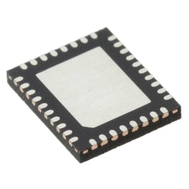
àà 36-pin TQFN (ZF)
The PI2EQXDP101-A is a one Input and one Output DisplayPort™
ReDriver™ that support a maximum data rate of 2.7 Gbps through
each channel, which results in a total of 10.8Gbps through-put.
Output Level Swing and Output Pre-emphasis and number of
active lanes are controlled by decoding the AUX command
during link initialization. Also, utilizing the HPD signals from
each DisplayPort port, the PI2EQXDP101-A can automatically
enter power down state. Or, if the graphics driver is off and has
no output signal, Pericom’s PI2EQXDP101-A can automatically
enter low power mode, even if an active monitor is attached.
Bias
DDC_SCL/AUX+
DDC_SDA/AUX-
AUX CH
interpreter
register
10-0194
AUX_SRC-
VDD15
AUX_SRC+
DDC_SCL/AUX+
DDC_SCL
31
30
29
28
OUT0+
IN0- 2
27
OUT0-
IN1+ 3
26
OUT1+
IN1- 4
25
OUT1-
VDD15 5
24
GND
IN2+ 6
23
OUT2+
IN2- 7
22
OUT2-
8
21
VDD15
IN3+ 9
20
OUT3+
19
OUT3-
11
12
13
14
15
16
17
18
GND
IN3- 10
1
DDC_SDA/AUX-
DDC_SDA
32
IN0+ 1
GND
DDC
Pass
through
33
VDD15
SDA
34
NC
SCL
35
HPD_Sink
AUX
Pass
through
36
CAD_Sink
AUX_SRC+
AUX_SRC-
OUT [3:0]±
HPDSRC
Logics
HPD SRC
CAD SRC
Pre-emphasis
CAD
HPD_Sink
CAD_Sink
Equalizer
VDD15
IN [3:0]±
Pin Diagram (Top-side View)
VDD33
Block Diagram
P-0.3
07/09/10
�PI2EQXDP101-A
1 to 1 DisplayPort™ ReDriver™
Pin Description
Pin #
Name
I/O
Description
33
32
12
14
34
AUX_SRC+
AUX_SRCCAD
CAD_Sink
DDC_SCL
I/O
I/O
Output
Input
I/O
31
DDC_SCL/AUX+
I/O
35
DDC_SDA
I/O
30
DDC_SDA/AUX-
I/O
Aux positive channel on source side
Aux negative channel on source side
Cable Detect to source
Cable Detect from DP connector, with 200K-Ohm pull-down.
I2C SCL clock on source side
Aux channel positive when configured as DP mode, I2C SCL clock
when configured as TMDS mode
I2C SDA data on source side
Aux channel negative when configured as DP mode, I2C SDA data
when configured as TMDS mode
GND
Power
Ground
HPD_Sink
HPDSRC
IN0+
IN0IN1+
IN1IN2+
IN2IN3+
IN3NC
OUT0+
OUT0OUT1+
OUT1OUT2+
OUT2OUT3+
OUT3VDD15
VDD33
Input
Output
Hot Plug detect from sink side, with 200K-Ohm pull-down.
Hot Plug detect to source
Input
Lane 0 data input, differential pair
Input
Lane 1 data input, differential pair
Input
Lane 2 data input, differential pair
Input
Lane 3 data input, differential pair
-
No Connect
Output
Lane 0 data output, differential pair
Output
Lane 1 data output, differential pair
Output
Lane 2 data output, differential pair
Output
Lane 3 data output, differential pair
Power
Power
Power Supply, 1.5V ± 5%
Power Supply, 3.3V ± 5%
8, 18, 24, Center
Pad
15
13
1
2
3
4
6
7
9
10
16
28
27
26
25
23
22
20
19
5, 11, 17, 21, 29
36
10-0194
2
P-0.3
07/09/10
�PI2EQXDP101-A
1 to 1 DisplayPort™ ReDriver™
AUX listener Register Assignment
AUX command are stored interpreted and stored in the registers, ReDriver will then be re-configured by default. Registers do not have a power-on default state.
Address
Name
Description
Link initialization field
AUX
LINK_BW_SET: Main Link Bandwidth Setting = Value x 0.27 Gbps per lane
Bits 7:0 = LINK_BW_SET
For DisplayPort version 1, revision 1a, only two values are supported. All
other values are reserved.
R/W
06h = 1.62 Gbps per lane
0Ah = 2.7 Gbps per lane
Source may choose either of the two link bandwidth as long as it does not exceed the capability of DisplayPort receiver as indicated in the receiver capability field.
Link initialization field
LANE_COUNT_SET
Bits3:0 = LANE_COUNT_SET
1h = One lane
2h = Two lanes
R/W
4h = Four lanes
For one-lane configuration, Lane0 is used. For 2-lane configuration, Lane0 and
Lane1 are used.
Bits7:4 = RESERVED. Read all 0’s.
00103h
DPCD Lane 0 status
TRAINING_LANE0_SET
Link Training Control_Lane0
Bits1:0 = DRIVE_CURRENT_SET
00 – Training Pattern 1 w/ level 0
01 – Training Pattern 1 w/ level 1
10 – Training Pattern 1 w/ level 2
11 – Training Pattern 1 w/ level 3
Bit2 = MAX_CURRENT_REACHED
Set to 1 when the maximum driven current setting is reached.
Note: Support of programmable drive current is optional. For
example if there is only 1 level, then program Bits2:0 to 100 to
indicate to the receiver that Level 1 is the maximum drive current.
Support of independent drive current controlfor each lane is also
optional.
Bit4:3 = PRE-EMPHASIS_SET
00 = Training Pattern 2 w/o pre-emphasis
01 = Training Pattern 2 w/ pre-emphasis level 1
10 = Training Pattern 2 w/ pre-emphasis level 2
11 = Training Pattern 2 w/ pre-emphasis level 3
Bit5 = MAX_PRE-EMPHASIS_REACHED
R/W
00104h
DPCD Lane 1 status
Lane setting for lane 1.
The definition is the same as lane 0
R/W
00105h
DPCD Lane 2 status
Lane setting for lane 2.
The definition is the same as lane 0
R/W
00106h
DPCD Lane 3 status
Lane setting for lane 3.
The definition is the same as lane 0
R/W
00100h
00101h
10-0194
Access
3
P-0.3
07/09/10
�PI2EQXDP101-A
1 to 1 DisplayPort™ ReDriver™
AUX listener specification
DP AUX command interpreter will support Native AUX CH Syntax. Mapping of I2C onto AUX CH Syntax is not supported.
AUX command interpreter monitor AUX channel from requester and replier for transactions and stored AUX command from requester and reply command from replier that are related to the link settings.
The data from the following addresses will be extracted and stored into internal registers for controlling the ReDriver signal level,
lane count and pre-emphasis setting.
00101h LANE_COUNT_SET
00103h TRAINING_LANE0_SET
00104h TRAINING_LANE1_SET
00105h TRAINING_LANE2_SET
00106h TRAINING_LANE3_SET
PI2EQXDP101
ReDriver
HPDSRC
DisplayPort
Transmitter
MAIN LINK
IN±
C
AUX
DDC
CAD
10-0194
4
HPD
OUT±
C
DP Connector
Application Diagram
DDC/AUX
CAD_SINK
P-0.3
07/09/10
�PI2EQXDP101-A
1 to 1 DisplayPort™ ReDriver™
Maximum Ratings
(Above which useful life may be impaired. For user guidelines, not tested.)
Storage Temperature......................................................... –65°C to +150°C
Supply Voltage to Ground Potential.................................... –0.5V to +4.6V
DC SIG Voltage...........................................................–0.5V to VDD +0.5V
Current Output ................................................................-25mA to +25mA
Power Dissipation Continuous........................................................ 500mW
Operating Temperature............................................................... 0 to +85°C
Note:
Stresses greater than those listed under MAXIMUM RATINGS may cause permanent damage to the device. This is
a stress rating only and functional operation of the device
at these or any other conditions above those indicated in
the operational sections of this specification is not implied.
Exposure to absolute maximum rating conditions for extended periods may affect reliability.
DC Electrical Characteristics (VDD33 = 3.3V ±5%, VDD15 = 1.5V ±5%, TA=0°C to 85°C)
Power Supply Characteristics
Symbol
Parameters
IACTIVE_VDD15
Current into VDD15 when active
ISTANDBY_VDD15 Current into VDD15 when standby
IACTIVE_VDD33
Current into VDD33 when active
ISTANDBY_VDD33
Current into VDD33 when standby
PACTIVE
Total active power
Pstandby
Total standby power
Condition
4-lanes operating at 2.7Gbps
4-lanes operating at 2.7Gbps
Input Low-level current
VOH
VOL
LVTTL high level output voltage
LVTTL low level output voltage
Typ.
150
Max.
250
10
Units
mA
mA
0.1
1.0
mA
0.1
mA
400
mW
20
mW
Typ.
Max.
43
0.8
80
Units
V
V
uA
6
20
uA
0.4
V
V
4-lane, operating 2.7Gbps
HPD_SRC, HPD_Sink , CAD, CAD_Sink, Pin Charaxteristics
Symbol
Parameters
Condition
VIH
LVTTL input high voltage
VIL
LVTTL input low voltage
IIH
Input High-level current
IIL
Min.
IOH=-8mA
IOL= 8mA
Min.
2
2.4
AUX_SRC±, DDC_SCL/AUX+, DDC_SDA/AUX– pins (When configured as SCL and SDA pins)
Symbol
Parameters
Condition
Min.
IIH
Input High-level current
IIL
Input Low-level current
Typ.
43
6
Max.
80
20
Units
uA
uA
AUX_SRC±, DDC_SCL/AUX+, DDC_SDA/AUX– pins (When configured as AUX± pins)
Symbol
Parameters
Condition
Min.
IIH
Input High-level current
10-0194
5
IIL
Input Low-level current
Typ.
43
6
Max.
80
P-0.3
20
Units
uA
07/09/10
uA
�PI2EQXDP101-A
1 to 1 DisplayPort™ ReDriver™
AUX Channel Electrical Specifications
Symbol
Parameter
VI
AUX Unit Interval
Pre-charge
pulses
Number of pre-charge
pulses
Sync Pulses
Number of sync pulses
VAUX-DIFFp-p
AUX Peak-to-peak Voltage at a VAUX-DIFFp-p
receiving Device
= 2*|VAUX+ – VAUX-|
AUXATTEN
VAUXP-DC
VAUXN-DC
IAUX_SHORT
AUX attenuation
AUX+ DC Voltage Range
AUX– DC Voltage Range
AUX Short Circuit Current
CAUX
AUX AC Coupling
Capacitor
10-0194
Conditions
1Mbps including overhead of
Mancester II coding
Each pulse is a ‘0’ in Manchester
II code.
Min
Nom
Max
Units
0.4
0.5
0.6
µS
10
16
16
0.32
with 100-Ohm termination
1.5
0
1.3
The AUX CH AC coupling
capacitor placed on the Display- 75
Port Source
6
1.36
V
2.0
2.0
3.3
90
dB
V
200
nF
mA
P-0.3
07/09/10
�PI2EQXDP101-A
1 to 1 DisplayPort™ ReDriver™
Main Link Receiver (Main RX) Specifications
Symbol
UI_High_Rate
UI_Low_Rate
VRX-DIFFp-p-HR
TRX-EYE-MEDIAN-toMAX-ITTER_CHIP
TRX-EYE_CONN
TRX-EYE_CHIP
TRX-EYE-MEDIAN-toMAX-JITTER_CHIP
Parameters
Unit Interval for high bit
rate (2.7 Gbps / lane)
Unit Interval for low bit
rate (1.62 Gbps / lane)
Differential Peak-to-peak Input
Voltage at RX package pins
Maximum time between
the jitter median and
maximum deviation from
the median at Rx package
pins
Minimum Receiver Eye Width
at RX-side connector pins
Minimum Receiver Eye Width
at RX package pins
Maximum time between the
jitter median and maximum
deviation from the median at RX
package
pins
VRX-DC-CM
RX DC Common Mode Voltage
ZRX-DC
DC Input Resistance
Differential Return Loss at
0.675GHz at RX package pins
Differential Return Loss at
1.35GHz at RX package pins
RLRX-DIFF
LRX-SKEWINTER_PAIR
LRX-SKEWINTRA_PAIR HighBit-Rate
LRX-SKEWINTRA_PAIR_Reduced-Bit-Rate
Lane-to-Lane Output Skew at
RX package pins
Lane Intra-pair Output Skew at
RX package pins
Lane Intra-pair Output Skew at
RX package pins
Comments
Min.
Range is nominal +/-350ppm.
DisplayPort link RX does not
require local crystal for link clock
generation.
For High Bit Rate. Informative.
Typ.
Max.
Units
370
ps
617
ps
120
1500
mV
0.265
UI
Note 1
0.25
UI
Note 1
0.22
UI
Note 1
Common mode voltage is equal to
Vbias_Rx voltage
0
45
Straight loss line between 0.675
GHz and 1.35 GHz
Straight loss line between 0.675
GHz and 1.35 GHz
Maximum skew limit between
different RX lanes of a
DisplayPort link.
For High Bit Rate Maximum skew
limit between D+ and D- of the
same lane.
For Reduced Bit Rate
Maximum skew limit between
D+ and D- of the same lane.
50
0.39
UI
2.0
V
55
12
dB
9
dB
5200
ps
100
ps
300
ps
Note:
1. For Reduced Bit Rate (1- TRX-EYE_CONN) specifies the allowable TJ. TRX-EYE-MEDIAN-to-MAX-JITTER specifies the total allowable DJ
10-0194
7
P-0.3
07/09/10
�PI2EQXDP101-A
1 to 1 DisplayPort™ ReDriver™
Main Link Transmitter (Main TX) Specifications
Symbol
UI_High_Rate
UI_Low_Rate
VTX-DIFFp-p
VTX-PREEMP-
Parameters
Unit Interval for high bit rate (2.7 Gbps /
lane)
Unit Interval for low bit rate (1.62 Gbps
/ lane)
Differential Peak-to-peak Output Voltage
Output Pre-emphasis ratio
RATIO
TTX-EYE_CHIP
Comments
High limit = +300ppm
Low limit = -5300ppm
HBR, VDD15 = 1.5V
Voltage level 1
Voltage level 2
Voltage level 3
Voltage level 4
HBR, VDD15 = 1.5V
No pre-emphasis
3.5 dB pre-emphasis
6.0 dB pre-emphasis
9.5 dB pre-emphasis
Minimum TX Eye Width at Tx package
pins
For High Bit Rate
Maximum time between the jitter median
and maximum deviation from the median
at Tx package pins
For High Bit Rate
Minimum TX Eye Width at Tx package
pins
For Reduced Bit Rate
MEDIAN-to-MAXJITTER_CHIP__
Low_Rate
Minimum TX Eye Width
at Tx package pins
For Reduced Bit Rate
TTX-RISE_CHIP,
TTX-FALL_CHIP
D+/D- TX Output Rise/Fall
Time at Tx package pins
At 20%-to-80%
VTX-DC-CM
TX DC Common Mode Voltage
VTX-AC-CM
TX AC Common Mode Voltage
ITX-SHORT
TX Short Circuit Current Limit
RLTX-DIFF
Differential Return Loss at 0.675GHz at
TX package pins
Differential Return Loss at 1.35GHz at
TX package pins
_High_Rate
TTX-EYEMEDIAN-to-MAXJITTER_CHIP__
High_Rate
TTX-EYE_CHIP
_Low_Rate
TTX-EYE-
Min.
Common mode voltage is equal
to Vbias_Tx voltage shown in
Differential Waveform
Measured at 1.62 GHz and
2.7 GHz (if supported), within
the frequency tolerance range.
Time-domain measurement using a spectrum analyzer.
Total drive current of the transmitter when it is shorted to its
ground.
Straight loss line between 0.675
GHz and 1.35 GHz
Straight loss line between 0.675
GHz and 1.35 GHz
Typ.
Max.
Units
370
ps
617
ps
340
340
510
690
1020
0.0
400
600
800
1200
0.0
2.8
4.8
7.6
0.0
3.5
6.0
9.5
1380
mV
460
680
920
1380
11.4
dB
0.0
4.2
7.2
11.4
0.726
UI
0.137
0.82
UI
UI
0.09
UI
50
130
ps
0
1.5
V
20
mV
50
mA
12
dB
9
dB
(Continued)
10-0194
8
P-0.3
07/09/10
�PI2EQXDP101-A
1 to 1 DisplayPort™ ReDriver™
Symbol
LTX-SKEWINTER_PAIR
LTX-SKEWINTRA_PAIR
Parameters
Lane-to-Lane Output Skew at Tx package
pins
Lane Intra-pair Output Skew at Tx package pins
TTX-RISE_FALL
_MISMATCH
_CHIPDIFF
Lane Intra-pair Rise-fall Time Mismatch
at Tx package pins.
CTX
AC Coupling Capacitor
JTOTAL
Total Output Jitter
Comments
Min.
Informative. D+ rise to D- fall
mismatch and D+ fall to D- rise
mismatch.
All DisplayPort Main Link lanes
as well as AUX CH must be AC
coupled. AC coupling
capacitors must be placed on the 75
transmitter side. Placement
of AC coupling capacitors the
receiver side is optional.
Typ.
Max.
Units
2
UI
20
ps
5
%
200
nF
0.32
UIp-p
Notes:
1. Refer to Pre-emphasis waveform. For embedded connection, support of programmable voltage swing levels is optional.
2. Refer to Pre-emphasis waveform for definition of differential voltage. Support of no preemphasis, 3.5 dB and 6.0 dB pre-emphasis is required.
Support of 9.5 dB level is optional. For embedded connection, support of programmable preemphasis levels is optional.
10-0194
9
P-0.3
07/09/10
�PI2EQXDP101-A
1 to 1 DisplayPort™ ReDriver™
Pre-emphasis = 20.Log(VDIFF-PRE/VDIFF)
VD+
Common Mode
Voltage
VCM
VDIFF
VD+
VD-
VDIFFp-p
V_D+ - V_D-
0V
VCM
VDIFF-PRE
VDIFF
VD-
VDIFFp-p
1stTBIT
2nd +TBIT(s)
Definition of Differential Voltage and Differential Voltage Peak-to-Peak
Definition of Pre-emphasis
Output Waveform (400mV, 0dB pre-emphasis)
Output Waveform (400mV, 6dB pre-emphasis)
Output Eye Diagram (2.7Gbps, 400mV)
Output Eye Diagram (2.7Gbps, 1200mV)
10-0194
10
P-0.3
07/09/10
�PI2EQXDP101-A
1 to 1 DisplayPort™ ReDriver™
Packaging Mechanicals: 36 Contact, TQFN (ZF)
DATE: 03/10/09
DESCRIPTION: 36-contact, Very Thin Fine Pitch Quad Flat No-Lead (TQFN)
PACKAGE CODE: ZF (ZF36)
DOCUMENT CONTROL #: PD-2023
REVISION: C
09-0143
Ordering Information
Ordering Code
Package Code
PI2EQXDP101-AZFE
ZF
Package Description
36-Contact, Pb-Free & Green (TQFN)
Notes:
• Thermal characteristics can be found on the company web site at www.pericom.com/packaging/
• E = Pb-free and Green
• Adding an X suffix = Tape/Reel
10-0194
11
Pericom Semiconductor Corporation • 1-800-435-2336 • www.pericom.com
P-0.3
07/09/10
�


 工商网监
湘ICP备2023018690号
工商网监
湘ICP备2023018690号
