PI3G612
1.8/3.3V High-Bandwidth 6-channel,
2:1 Mux/DeMux with switched Pull-ups
Description
Features
The PI3G612 is a 3-port, 6-channel, 1:2 multiplexer/demultiplexer.
It features switched 100 K-Ohm active pull-ups on output ports A
and B to prevent disconnected floating signals and thereby reduce
system noise and power. The Y port can be connected to either the A
or B ports, or alternatively both ports can be isolated, disconnected,
or all connected. When the EP pin is low, the pull-up transistors
are off. When EP is high, the pull-up transistors are on. If EP is not
connected, an internal pull-down will turn the pull-up off. If pullups are not used, EP should be connected to ground. The PI3G612
has a wide operating voltage range, very low power consumption
and small packaging suitable for mobile, and handheld equipment.
• Near-Zero propagation delay
•
•
•
•
•
•
•
•
•
5Ω switches connect inputs to outputs
Signal passing bandwidth, 400 MHz
Rail-to-Rail™ switching
1.8V to 3.3V supply voltage operation
Supports live insertion and hot-swap
Industrial operating temperature: -40ºC to +85ºC
2KV ESD HBM
Latch-up performance >250mA per JESD17
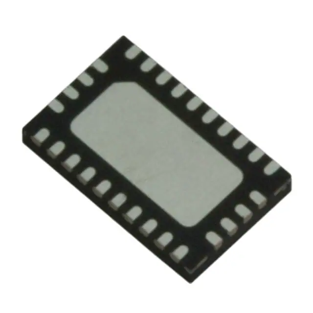
Packaging: 28-contact TQFN (3.5 x 5.0, 0.5mm pad pitch)
Block Diagram
Applications
EP
• Memory card switching
SA
SB
• Photo printers
• Mobile devices
CONTROL
DECODER
Y0
A0
B0
Pin Configuration (Top-side view)
B0
25
A0
28 27 26
EP
VDD
Y1
B1
24
A1
23
B1
3
22
GND
Y2
4
21
A2
VDD
5
20
B2
Y3
6
19
VDD
GND
7
18
A3
Y4
8
17
B3
Y5
9
16
A4
SB
10
15
B4
GND
GND
11 12 13
14-0062
14
Y2
A2
B2
Y3
A3
B3
Y4
A4
B4
Y5
A5
2
VDD
Y1
B5
1
SA
Y0
A1
A5
B5
1
www.pericom.com 04/29/14
�PI3G612
1.8/3.3V High-Bandwidth 6-channel,
2:1 Mux/DeMux with switched Pull-ups
Pin Description
Pin Name
Description
AX, BX, YX
Data I/O
SA, SB
Channel Select Inputs
EP
Pull-ups Enable
GND
Ground
VDD
Power
Truth Table
Control Inputs
EP
SB
0
0
0
0
0
1
0
1
1
0
1
1
1
0
1
1
SA
0
1
0
1
0
Switch State1
Bx
Open
Open
Closed
Closed
Open
1
0
1
Open
Closed
Closed
Pullup State
Function2
Ax
Open
Closed
Open
Closed
Open
Off
Off
Off
Off
On
Closed
Open
Closed
On
On
On
Y, A, B all disconnected and Hi-Z
Y=A, B =Hi-Z
Y=B, A =Hi-Z
Y=A=B
Y, A, B all disconnected; Y=Hi-Z; A & B pull to
VDD
Y=A; A & B pull toVDD
Y=B; A& B pull to VDD
Y=A=B; A& B pull to VDD
Notes:
1. For the group of 6 transistor switches connecting to the Ax or Bx signals.
2. Function for stand-alone device (no other signal source connected)
14-0062
2
www.pericom.com 04/29/14
�PI3G612
1.8/3.3V High-Bandwidth 6-channel,
2:1 Mux/DeMux with switched Pull-ups
Maximum Ratings
(Above which the useful life may be impaired. For user guidelines, not tested.)
Storage Temperature................................................. –65°C to +150°C
Ambient Temperature with Power Applied................ –40°C to +85°C
Supply Voltage to Ground Potential ........................... –0.5V to +4.6V
DC Input Voltage......................................................... –0.5V to +6.0V
DC Output Current.................................................................... 120mA
Note:
Stresses greater than those listed under MAXIMUM
RATINGS may cause permanent damage to the device. This is a
stress rating only and functional operation of the device at these or
any other conditions above those indicated in the operational sections
of this specification is not implied. Exposure to absolute maximum
rating conditions for extended periods may affect reliability.
Power Dissipation.........................................................................0.5W
DC Electrical Characteristics, 3.3V Supply (Over the Operating Range, TA = –40°C to +85°C, VDD = 3.3V ±10%)
Parameters
Description
Test Conditions(1)
Typ(2)
Min.
Max.
Units
0.8
V
VIH
Input HIGH Voltage
Guaranteed Logic HIGH Level
2.0
VIL
Input LOW Voltage
Guaranteed Logic LOW Level
–0.5
VIK
Clamp Diode Voltage
Vdd = Min., IIN = –18 mA
IIH
Input HIGH Current
Vdd = Max., VIN = Vdd
±1
IIL
Input LOW Current
Vdd = Max., VIN = GND
±1
IOZH
High Impedance Output Current 0 ≤ Y, In ≤ VDD
RON
Switch
On-Resistance(3)
–0.75
–1.2
µA
±25
Vdd = Min., VIN = 0V,
ION = 24mA
Vdd = Min., VIN = 2.4V, ION = 12 mA
2
3.3
2.6
4.3
Ohm
DC Electrical Characteristics, 1.8V Supply (Over Operating Range, TA = –40°C to +85°C, VDD = 1.8V ± 10%)
Parameters(4)
Description
Test Conditions (1)
Min.
Typ. (2)
Max.
VIH
Input HIGH Voltage
Guaranteed Logic HIGH Level
1.1
–
VDD + 0.3
VIL
Inout LOW Voltage
Guaranteed Logic LOW Level
–0.3
–
0.5
VIK
Clamp Diode Voltage
VDD = Max., IIN = –6mA
–
–0.7
–1.8
IIH
Input HIGH Current
VDD = Max., VIN = VDD
–
–
±1
IIL
Input LOW Current
VDD = Max., VIN = GND
–
–
±1
IOZH
High Impedance Current
0 ≤ Y, In ≤ VDD
–
–
±10
VDD = 1.5V, VIN = 0V,
ION = 24mA
–
2.6
4
VDD = 1.5V, VIN = 1.3V,
ION = 12mA
–
Switch On-Resistance(3)
RON
Units
V
µA
Ohm
5.5
8
Notes:
1. For Max. or Min. conditions, use appropriate value specified under Electrical Characteristics for the applicable device type.
2. Typical values are at nominal VDD, TA = 25°C ambient and maximum loading.
3. Measured by the voltage drop between Y and In pin at indicated current through the switch. On-Resistance is determined
by the lower of the voltages on the two (Y, In) pins.
4. This parameter is determined by device characterization but is not production tested.
14-0062
3
www.pericom.com 04/29/14
�PI3G612
1.8/3.3V High-Bandwidth 6-channel,
2:1 Mux/DeMux with switched Pull-ups
Capacitance (TA = 25°C f = 1 MHz)
Parameters
Description
Test Conditions
CIN
Input Capacitance (Control)
COFF(IN)
In Capacitance, Switch Off
CON
In Capacitance, Switch On
Power Supply Characteristics
Parameters
Quiescent Power Supply Current
Vcontrol (EP, SB, SA) = GND or
VDD
ICC
Units
2
VIN = 0V
4
pF
15
Test Conditions(1)
Description
Typ.
Min.
Typ.
Max.
VDD = 3.3 V
120
VDD = 1.8 V
10
Units
µA
Notes:
1. For Max. or Min. conditions, use appropriate value specified under Electrical Characteristics for the applicable device.
Dynamic Electrical Characteristics Over the Operating Range (TA = -40º to +85º, VDD = 3.3V ± 10%)
Parameter
Description
Test Condition
BW
-3dB Bandwidth
See Test Diagram (CL = 0pF)
Switching Characteristics over 3.3V Operating Range
Parameters
Description
Delay(2,3) Y to
tPLH
tPHL
Propagation
to Y
tPZH
tPZL
Enable Time S to (Y, A or B)
tPHZ
tPLZ
Disable Time S to (Y, A or B)
(A or B), (A or B)
Conditions(1)
Min.
Typ.
Max.
400
Min.
See Test Diagram
Units
MHz
Max.
Units
0.3
1.5
10
1.5
10
Min.
Max.
ns
See Test Diagram
Switching Characteristics over 1.8V Operating Range
Parameters
Description
Delay(2,3) Y to
tPLH
tPHL
Propagation
or B) to Y
tPZH
tPZL
Enable Time S to (Y, A, or B)
tPHZ
tPLZ
Disable Time S to (Y, A, or B)
(A, or B), or (A,
Conditions(1)
See Test Diagram
Units
0.3
1.5
25.0
1.5
25.0
ns
See Test Diagram
Notes:
1. See test circuit and waveforms.
2. This parameter is guaranteed but not tested on Propagation Delays.
3. The switch contributes no propagational delay other than the RC delay of the On-Resistance of the switch and the load
capacitance. The time constant for the switch alone is of the order of 0.30ns for 10pF load. Since this time constant is much
smaller than the rise/fall times of typical driving signals, it adds very little propagational delay to the system. Propagational
delay of the switch when used in a system is determined by the driving circuit on the driving side of the switch and its
interaction with the load on the driven side.
14-0062
4
www.pericom.com 04/29/14
�PI3G612
1.8/3.3V High-Bandwidth 6-channel,
2:1 Mux/DeMux with switched Pull-ups
Test Circuit for Electrical Characteristics(1-5)
2 x VDD
VDD
200-ohm
VIN
Pulse
Generator
VOUT
D.U.T
10pF
CL
RT
200-ohm
Notes:
1. CL = Load capacitance: includes jig and probe capacitance.
2. RT = Termination resistance: should be equal to ZOUT of the Pulse Generator
3. Waveform 1 is for an output with internal conditions such that the output is low except when disabled by the output control.
Waveform 2 is for an output with internal conditions such that the output is high except when disabled by the output control.
4. All input impulses are supplied by generators having the following characteristics: PRR ≤ MHz, ZO = 50Ω, tR ≤ 2.5ns, tF ≤ 2.5ns.
5. The outputs are measured one at a time with one transition per measurement.
Switching Waveforms
1.8V
S or EP
2.5V
Input
0V
2.5V
tPLH
tPHL
1.5V
Waveform 1
Output
tPZL
tPLZ
VDD/2
VOH
Output
2.5V
0.9V
0.9V
3.5V
2.5V
VOL
Waveform 2
VOH
VOL +0.3V
VOL
tPHZ
tPZH
VOH
VDD/2
Output
VOH -0.3V
VOL
Voltage Waveforms Enable and Disable Times
3.5V
2.5V
Input
tPLH
tPHL
1.5V
VOH
2.5V
Output
VOL
tSK(p) = I tPHL – tPLH I
Pulse Skew - tSK(p)
14-0062
5
www.pericom.com 04/29/14
�PI3G612
1.8/3.3V High-Bandwidth 6-channel,
2:1 Mux/DeMux with switched Pull-ups
Switch Positions
Test
Switch
tPLZ, tPZL
2 x VDD
tPHZ, tPZH
GND
Prop Delay
Open
Test Circuit for Dynamic Electrical Characteristics
HP4396
S1
VCC
R1
T1
D.U.T
HP11667A
CL
Applications Information
Logic Inputs
The logic control inputs can be driven up to 3.6V regardless of the supply voltage. For example, given a +3.3V supply, SA or SB
maybe driven LOW to 0V and HIGH to 3.6V. Driving SA or SB Rail-to-Rail® minimizes power consumption.
14-0062
6
www.pericom.com 04/29/14
�PI3G612
1.8/3.3V High-Bandwidth 6-channel,
2:1 Mux/DeMux with switched Pull-ups
Packaging Mechanical: 28-pin TQFN (ZH)
DATE: 07/11/12
DESCRIPTION: 28-Contact, Very Thin Quad Flat No-Lead, TQFN
PACKAGE CODE: ZH28
REVISION: C
DOCUMENT CONTROL #: PD-2034
12-0419
Note: For latest package info, please check: http://www.pericom.com/products/packaging/mechanicals.php
Ordering Information
Ordering Code
PI3G612ZHE
Package Code
ZH
Package Description
28-contact, Very Thin Quad Flat No-Lead (TQFN)
Notes:
• Thermal characteristics can be found on the company web site at www.pericom.com/packaging/
• E = Pb-free and Green
• X suffix = Tape/Reel
Pericom Semiconductor Corporation • 1-800-435-2336 • www.pericom.com
14-0062
7
www.pericom.com 04/29/14
�


 工商网监
湘ICP备2023018690号
工商网监
湘ICP备2023018690号
