A product Line of
Diodes Incorporated
PI3WVR31212A
DP/HDMI 1:2 De-multiplexer switches
Features
Description
ÎÎDP/HDMI 1:2 De-multiplexer switch with 4 high speed
PI3WVR31212A has one passive output port1, one active (DP to
HDMI) output port2. Passive output supports DP1.2 at 5.4Gbps
in I2C mode. Active port2 supports HDMI1.4b at 3.4Gbps.All
two output ports support auto port priority selection. Input port
accepts DP1.2 and DP++ signals associated with output ports as
described above.
differential channel and AUX/DDC, HPD and CAB_DET
signal channels
ÎÎOne passive output ports for DP1.2 at 5.4Gbps
ÎÎOne active output port with integrated DP to HDMI re-
driver (level shifter) supports HDMI 1.4 at 3.4Gbps
ÎÎPin control mode supports auto port priority selection
Application
ÎÎPin control mode supports port2 with DDC bi-direction
buffer switch only
ÎÎNotebook and dongle
ÎÎI2C control mode supports auto port priority selection
ÎÎI2C control mode supports port2 with 8 levels equalization
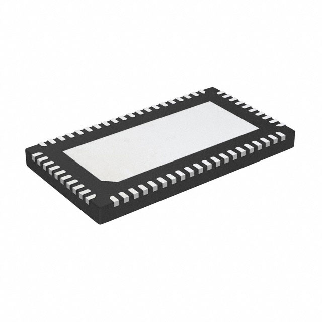
Pin Configuration: TQFN-60
and 5 levels pre-emphasis
AUXN
AUXP
SCL2
SDA2
GND
GND
NC
AUX1P/SCL1
AUX1N/SDA1
CAB_1
ÎÎI2C control mode supports port2 with either DDC bi-
direction buffer switch or DDC passive switch
ÎÎVery low operating power when passive port1 is selected
ÎÎ3.3V power supply
ÎÎ2KV HBM ESD protection for all I/O pins
60 59 58 57 56 55 54 53 52 51
OEB
SCL
SDA
VDD
HPD_SRC
CAB_SRC
D0P
D0N
D1P
D1N
D2P
D2N
D3P
D3N
SDA_CTL/PRI_SEL
SCL_CTL/EQ
I2C_A1/PRE_EMP
I2C_A2/ROUT_SEL
HPD2
GND
ÎÎSupport Type 2 cable ID register
ÎÎPackaging:
60 pin TQFN package (5x9mm, 0.4mm pitch)
1
2
3
4
5
6
7
8
9
10
11
12
13
14
15
16
17
18
19
20
Center Pad
TQFN-60
5x9 mm
50
49
48
47
46
45
44
43
42
41
40
39
38
37
36
35
34
33
32
31
VDD
D0P1
D0N1
D1P1
D1N1
D2P1
D2N1
D3P1
D3N1
GND
NC
NC
NC
GND
NC
NC
GND
CEXT
HPD1
MS
CLKN2
CLKP2
VDD
D0N2
D0P2
D1N2
D1P2
VDD
D2N2
D2P2
21 22 23 24 25 26 27 28 29 30
All trademarks are property of their respective owners.
17-0054
1
www.diodes.com 03/28/17
�A product Line of
Diodes Incorporated
PI3WVR31212A
Block Diagram
CEXT
CAB_SRC HPD_SRC
HPD1
120KΩ
VDD
LDO
HPD2
120KΩ
CAB_1
100KΩ pull High
AUXP
AUXN
AUX1P/SCL1
AUX1N/SDA1
SDA
SCL
SDA2
SCL2
Cable ID
D[0:3]P1
D[0:3]N1
VDD
0//VDD
D[0:3]P
D[0:3]N
RT
Port select
RT
ROUT
ROUT
D[0:3]P2
D[0:3]N2
Rpd
Rpd
GND
OEB
MS
PRI_SEL
EQ
PRE_EMP
ROUT_SEL
Control & Status
Register
I2C
Controller
SDA_CTL
SCL_CTL
(share pins)
I2C_A1, A2
(share pins)
All trademarks are property of their respective owners.
17-0054
2
www.diodes.com 03/28/17
�A product Line of
Diodes Incorporated
PI3WVR31212A
Pin Description
Pin#
Pin Name
7
D0P
9
D1P
11
D2P
13
D3P
8
D0N
10
D1N
12
D2N
14
D3N
49
D0P1
47
D1P1
45
D2P1
43
D3P1
48
D0N1
46
D1N1
44
D2N1
42
D3N1
25
D0P2
27
D1P2
30
D2P2
22
CLKP2
24
D0N2
26
D1N2
29
D2N2
21
CLKN2
52
AUX1N/SDA1
53
AUX1P/SCL1
57
SDA2
58
SCL2
60
AUXN
59
AUXP
3
SDA
2
SCL
32
HPD1
I
19
HPD2
I
5
HPD_SRC
O
All trademarks are property of their respective owners.
Signal Type Description
17-0054
IO
4 differential pair input (DP)
IO
4 differential pair output (DP) for port 1
IO
4 differential pair output (HDMI) for port 2
IO
AUX (DP) or DDC (HDMI) to two ports
IO
AUX to DP-source
IO
DDC to DP-source
HPD1-2 for port1-2;
HPD_SRC to DP-source.
3
www.diodes.com 03/28/17
�A product Line of
Diodes Incorporated
PI3WVR31212A
Pin#
Pin Name
51
CAB_1
6
CAB_SRC
1
OEB
I
15
SDA_CTL/PRI_SE
I
16
SCL_CTL/EQ
17
I2C_A1/PRE_EMP
18
Signal Type Description
CAB_1: CAB_DET to port1
IO
CAB_SRC: CAB_DET to DP-source
No CAB_DET for HDMI port2
OEB=0, device active; OEB=1, device shut down
MS=0, PRI_SEL selects priority in pin control mode;
MS=1, SDA_CTL as SDA in I2C control mode
MS=0, EQ selects equalization in pin control mode;
IO
I2C_A2/ROUT_SEL
MS=1, SCL_CTL as SCL in I2C control mode
MS=0, PRE_EMP selects Pre-emphasis in pin control mode;
I
MS=1, I2C_A1 as I2C address A1 in I2C control mode
MS=0, ROUT_SEL selects source termination in pin control
mode;
I
MS=1, I2C_A2 as I2C address A2 in I2C control mode
Mode Select:
31
MS
I
MS=0 for pin control mode
MS=1 for I2C control mode
33
CEXT
O
4, 23, 28, 50
VDD
Power
20, 34, 37, 41, 55, 56,
Center Pad
GND
Ground
35, 36, 38, 39, 40, 54
NC
All trademarks are property of their respective owners.
Internal LDO bypass capacitance, 4.7uf to GND
3.3V VDD
Bottom GND EPAD
NC
17-0054
Not Connected
4
www.diodes.com 03/28/17
�A product Line of
Diodes Incorporated
PI3WVR31212A
Pin mapping for dual mode DP source DEMUX to DP output
DP mode
HDMI/DVI mode WVR31212A input pins WVR31212A port1 output WVR31212A port2 output
ML_lane
TX2+
D0P
D0P1
D2P2
ML_lane
TX2-
D0N
D0N1
D2N2
ML_lane
TX1+
D1P
D1P1
D1P2
ML_lane
TX1-
D1N
D1N1
D1N2
ML_lane
TX0+
D2P
D2P1
D0P2
ML_lane
TX0-
D2N
D2N1
D0N2
ML_lane
TXC+
D3P
D3P1
CLKP2
ML_lane
TXC-
D3N
D3N1
CLKN2
Function Description
The MS pin selects I2C or pin control mode.
Pin control mode has only automatic port selection. I2C control mode has automatic port selection.
In auto port selection, when only one HPD high detected, the port with HPD high will be selected. When multiple HPD high detected,
the PRI_SEL pin (priority select) will determine the priority of the 2 ports. See priority selection table
When PRI_SEL=low or High, the port-priority will be port1-port2 from high to low; when PRI_SEL=M (open as not connected), the
port priority will be port2-por1 from high to low.
When port 1 is selected and CAB_1 is low as in DP mode, the AUX/DDC channels will work as AUX channels. AUXP shall have
100Kohm external resistor to GND and AUXN shall have 100Kohm external resistor to VDD. The data rate of AUX channels will be
>720Mbps.The internal DDC switch will be off.
When port 1 is selected and CAB_1 is high when DP to HDMI adapter plugged, the AUX/DDC channels will work as DDC channels.
The internal DDC channels are on and the AUX channels are off. The input of DDC channels can tolerate 5V input and voltage of
DDC to source will be limited about 3.3V or below.
When port 1 is selected (passive ports), port2 with HDMI re-driver will shut down.
When port 2 is selected, the internal DP to HDMI level shifter will be enabled. There will be 3 EQ and 3 Pre-emphasis settings in pin
control mode, 8 EQ and 5 Pre-emphasis settings in I2C control mode.
When port 2 is selected, HDMI output can be standard TMDS-open-drain source, as well to be selected with internal source termination as 50 ohm pull up to 3.3V VDD, using ROUT_SEL pin control or I2C control.
When port 2 is active as DP to HDMP level shifter, the DDC channel can be selected between bi-direction DDC buffer and passive
DDC switch in I2C mode.
HPD1, HPD2 are with internal CMOS buffers and can support 3.3V and 5V HPD inputs.
Squelch Mode
Squelch function will disable HDMI data output (as high impedance)when the voltage and frequency of input clock (TMDS) are
below squelch threshold, which will prevent random noise presenting in HDMI data output, thereby prevent noise on sink display.
Squelch function will enable-resume HDMI data output when input clock signals are above squelch threshold.
All trademarks are property of their respective owners.
17-0054
5
www.diodes.com 03/28/17
�A product Line of
Diodes Incorporated
PI3WVR31212A
Truth Table for TMDS port2
EQ – three level pin control
PRE-EMP – three level pin control
EQ
Equalization value
PRE_EMP
TX pre-emphasis
0
1.5dB
0
0dB
open
4.0dB
open
1.5dB
1
6.5dB
1
2.5dB
MS – three level pin control
ROUT_SEL
ROUT_SEL
Pull-Up Resistors on port2 D[0:2]P2/N2, CLKP2/N2
MS
Pin mode/type cable ID
0
No Pull-up resistors
0
Pin mode for Type 2 ID
1
50Ω Pull-up resistors to VDD
M(0.5*vdd)
Pin mode for Type 1 ID
1
I2C mode
Truth Table for AUX and DDC
PORT
When Port1 Selected
DP/HDMI
CAB_1
AUXP
AUXN
SCL
SDA
DP Mode
0
AUX1P
AUX1N
Hi-Z
Hi-Z
DP Mode
1
Hi-Z
Hi-Z
SCL1
SDA1
Priority Selection Table
PRI_SEL
(Priority order)
HPD1
HPD2
HPD_SRC
CAB_SRC
AUXP/AUXN
SDA/SCL
0 or 1
0
0
Hi-Z
Hi-Z
Hi-Z
Hi-Z
0 or 1
1
x
HPD1
CAB1
AUX1P/AUX1N
SDA1/SCL1
0 or 1
0
1
HPD2
High
Hi-Z
SDA2/SCL2
M
0
0
Hi-Z
Hi-Z
Hi-Z
Hi-Z
M
1
0
HPD1
CAB1
AUX1P/AUX1N
SDA1/SCL1
M
x
1
HPD2
High
Hi-Z
SDA2/SCL2
Note: M=internal half VDD when input=HiZ
PRI_SEL
(Priority order)
HPD1
HPD2
D0P
D1P
D2P
D3P
D0N
D1N
D2N
D3N
0 or 1
0
0
Hi-Z
Hi-Z
Hi-Z
Hi-Z
Hi-Z
Hi-Z
Hi-Z
Hi-Z
0 or 1
1
x
D0P1
D1P1
D2P1
D3P1
D0N1
D1N1
D2N1
D3N1
0 or 1
0
1
D2P2
D1P2
D0P2
CLKP2
D2N2
D1N2
D0N2
CLKN2
M
0
0
Hi-Z
Hi-Z
Hi-Z
Hi-Z
Hi-Z
Hi-Z
Hi-Z
Hi-Z
M
1
0
D0P1
D1P1
D2P1
D3P1
D0N1
D1N1
D2N1
D3N1
M
x
1
D2P2
D1P2
D0P2
CLKP2
D2N2
D1N2
D0N2
CLKN2
Note: M=internal half VDD when input=HiZ
All trademarks are property of their respective owners.
17-0054
6
www.diodes.com 03/28/17
�A product Line of
Diodes Incorporated
PI3WVR31212A
Maximum Ratings
(Above which useful life may be impaired. For user guidelines, not tested.)
Storage Temperature ........................................................... –65°C to +150°C
Junction Temperature............................................................................. 125°C
Supply Voltage to Ground Potential ....................................–0.5V to +4.6V
High Speed Channel Input Voltage (DP Mode)........................–0.5V to 2V
DDC and HPD channels Input Voltage ....................................–0.5V to 6V
DC Output Current ..............................................................................180mA
Power Dissipation .................................................................................... 0.6W
Note: Stresses greater than those listed under MAXIMUM
RATINGS may cause permanent damage to the device.
This is a stress rating only and functional operation of the
device at these or any other conditions above those indicated in the operational sections of this specification is not
implied. Exposure to absolute maximum rating conditions
for extended periods may affect reliability.
Electrical Characteristics
Recommended Operation Conditions
VDD = 3.3V ±10%, Min and Max apply for TA between -40oC to 85oC Typical values are referenced to TA = 25oC
Parameter
Description
VDD
Operating Voltage
Test Conditions
VDD supply current
(Port1 active)
IDD
VDD Supply Current
(Port2 active)
IDDQ
VDD Quiescent Supply Current
(port2 active w/o TMDS input)
Min.
Typ.
Max.
Unit
3.0
3.3
3.6
V
VDD=3.3V
1
1.8
mA
Output Enable ( open drain 500mv
signal-end 0dB pre-emphasis, not
including 40mA current to source)
80
100
mA
Output Enable ( double termination,
500mv signal-end 0dB pre-emphasis, not including 40mA current to
source)
160
200
mA
TMDS Output Disable,
3.5
5
mA
Isd1
Supply shut down current when
OEB disable (MS=0)
VDD=3.6V, OEB=high
0.1
0.2
mA
Isd2
Supply shut down current when
OEB disable (MS=1)
VDD=3.6V, OEB=high
0.6
1.2
mA
All trademarks are property of their respective owners.
17-0054
7
www.diodes.com 03/28/17
�A product Line of
Diodes Incorporated
PI3WVR31212A
DC Electrical Characteristics for Switching over Operating Range
Parameter
Description
Test Conditions
Min.
Typ.
Max.
Unit
OEB,MS,ROUT_SEL
IIH
High level digital input current
VIH =VDD
-10
40
μA
IIL
Low level digital input current
VIL = GND
-10
10
μA
VIH
High level digital input voltage
2.0
VIL
Low level digital input voltage
0
V
0.8
V
0.4
V
HPD_SRC
VOL_HPD_SRC
Buffer Output Low Voltage
IOL = 4 mA
VOH_HPD_SRC
Buffer Output Low Voltage
IOH = 4 mA
2.4
V
HPD_sink
IIH
High level digital input current(1) VIH =VDD
-10
40
μA
IIL
Low level digital input current(1)
VIL = GND
-10
10
μA
VIH
High level digital input voltage
VDD=3.3V
2.0
VIL
Low level digital input voltage
V
0
0.8
V
-50
50
uA
CAB
ILK
Input leakage current
Switch is off, Vin=5.5v
CIO
Input/Output capacitance whenpassive switch on
RON
Passive Switch resistance
IO = 3mA, VO = 0.4V
Vpass
Switch Output voltage
VI=3.3V, II=100uA
CI(source)
Source side CAB capacitance
CI(sink)
Sink side CAB capacitance when
10
1.5
VI peak-peak = 1V, 100 KHz
pF
25
50
Ω
3.0
3.3
V
3.5
pF
6.5
pF
SDA/SCL, SDA1/SCL1
ILK
Input leakage current
DDC switch is off, Vin=5.5V
CIO
Input/Output capacitance when
passive switch on
VI peak-peak = 1V, 100 KHz
8
RON
Passive Switch resistance
IO = 3mA, VO = 0.4V
25
50
Ω
Vpass
Switch Output voltage
2.0
2.5
V
CI(source)
Source side DDC capacitance (
passive switch off. )
CI(sink)
Sink side DDC capacitance ( pasVI peak-peak = 1V, 100 KHz
sive switch off. )
VI=5.0V, II=100uA
VDD=3.3V
-50
1.5
VI peak-peak = 1V, 100 KHz
50
uA
pF
2.5
pF
5
pF
SDA2/SCL2 ( DDC buffer of port2 active)
VIH
High level input voltage
VIL
Low level input voltage
ILK
Input leakage current
All trademarks are property of their respective owners.
VDD=3.3V
DDC switch is off, Vin = 5.5V
17-0054
8
2.0
V
0
0.8
V
-10
10
uA
www.diodes.com 03/28/17
�A product Line of
Diodes Incorporated
PI3WVR31212A
Parameter
Description
Test Conditions
IIL
Low level input current
VIL = 0.2V
VOL
Low level output voltage
ILOH
CIO
Min.
Typ.
Max.
Unit
10
μA
IOL = 4mA
0.2
V
HIGH-level output leakage current
VO=3.6V
10
μA
Input/output capacitance
VI = 3 V or 0 V; VCC = 3.3 V or 0V
-10
4
pF
SDA/SCL (DDC buffer of port2 active)
VIH
High level input voltage
VIL
Low level input voltage
ILK
Input leakage current
IIL
VDD=3.3V
2.0
V
0
0.4
V
DDC switch is off, Vin = 5.5V
-10
10
uA
Low level input current
VIL = 0.2V
-10
10
μA
VOL
Low level output voltage
IOL = 4mA
0.47
0.6
V
ILOH
HIGH-level output leakage current
VO=3.6V
10
μA
CIO
Input/output capacitance
VI = 3 V or 0 V; VCC = 3.3 V or 0V
0.52
5
8
pF
AUXP,AUXN, AUXnP/SCLn, AUXnN/SDAn
ILK
Input leakage current
DDC switch is off, Vin=5.5V
CIO
Input/Output capacitance when
passive switch on
VI peak-peak = 1V, 100 KHz
6
pF
RON
Passive Switch resistance
IO = 3mA, VO = 0.3V
5
Ω
IO = 3mA, VO = 3.0V
10
Ω
Vpass
Switch Output voltage
CI(source)
Source side capacitance ( passive
switch off. )
VI peak-peak = 1V, 100 KHz
2.5
pF
CI(sink)
Sink side capacitance ( passive
switch off. )
VI peak-peak = 1V, 100 KHz
3.5
pF
–1.6
VI=5.5V, II=100uA
VDD=3.3V
-50
50
4.0
4.5
uA
V
High Speed Channel (D[0:3]P/N – D[0:3]P1N1)
VIK
Clamp Diode Voltage (HS Channel)
VDD = Max., IIN = –18mA
IIH
Input HIGH Current
VDD = Max., VIN = VDD
±10
IIL
Input LOW Current
VDD = Max., VIN = GND
±10
RON_HS
On resistance between input to
out- put for high speed signals
VINPUT,cm = 0V to 1.8V,
VINPUT,diff < 1.0Vp-p, diff, VDD =
3.0V, IINPUT = 20mA
All trademarks are property of their respective owners.
17-0054
9
8
–1.8
V
µA
Ohm
www.diodes.com 03/28/17
�A product Line of
Diodes Incorporated
PI3WVR31212A
Parameter
Description
Test Conditions
Min.
Typ.
Max.
Unit
VDD+10
mV
50
66
ohm
30
100
uA
50
uA
Max.
Unit
High Speed Channel (D[0:3]P/N – D[0:2]P2/N2; CLKP2/N2)
VI(open)
Single-ended input voltage under
high impedance input or open
input
IL=10uA
VDD10
RT
Input termination resistance
VIN=2.9V
45
IOZ
Leakage current resistance
VDD=3.6V, OEB=High
Ioff
Power off leakage current
VDD=0, VIN=3.6V
-50
Dynamic Electrical Characteristics over Operating Range
(TA = -40º to +85ºC, VDD = 3.3V ±10%)
Parameter
Description
Test Conditions
Min.
Typ.
TMDS Differential Pins
tpd
tr
tf
Propagation delay
2000
Differential output signal rise time
120
(20% - 80%)
Differential output signal fall time
(20% - 80%)
VDD = 3.3V, Rout = 50Ω off, open
drain, 0dB pre-emphasis
120
tsk(p)
Pulse skew
15
50
tsk(D)
Intra-pair differential skew
25
50
tsk(o)
Inter-pair differential skew(2)
Tjit_clk(pp)
Peak-to-peak output jitter CLK
residual jitter
Tjit_dat(pp)
Peak-to-peak output jitter DATA
Residual Jitter
ten
Enable time
10
tdis
Disable time
50
ps
100
Data Input = 3.4 Gbps HDMI data
pattern from signal generation,
short trace.
CLK Input = 340 MHz clock
15
40
25
50
us
SCL,SDA channel, AUX channel , CAB channel : passive switches
tpd(DDC)
Propagation delay from SCLn/
SDAn to SCL/SDA or SCL/SDA to
SCLn/SDAn In passive SW on.
CL = 10pF, in passive switch
5
ns
SCL2,SDA2- SCL,SDA channel : buffers
tPLH
LOW-to-HIGH propagation delay
SCL/SDA to SCL2/SDA2
50
100
150
ns
tPHL
HIGH-to-LOW propagation delay
SCL/SDA to SCL2/SDA2
10
20
40
ns
tPLH
LOW-to-HIGH propagation delay
SCL2/SDA2 to SCL/SDA
50
100
150
ns
tPHL
HIGH-to-LOW propagation delay
SCL2/SDA2 to SCL/SDA
10
20
40
ns
All trademarks are property of their respective owners.
17-0054
10
www.diodes.com 03/28/17
�A product Line of
Diodes Incorporated
PI3WVR31212A
Parameter
Description
Test Conditions
Min.
Typ.
Max.
Unit
2
4
us
2
4
us
Typ.
Max.
Unit
Control and Status Pins (HPDn, HPD_SRC)
tpd(HPD)
Propagation delay (from HPDx to
the active port of HPD_SRC, high
to low)
tsx(HPD)
Switch time (from port select to
the latest HPD , manual selection
mode)
CL = 10pF
Dynamic Electrical Characteristics
Parameter
Description
Test Conditions
Min.
High Speed Channel (D[0:3]P/N – D[0:3]P1/N1)
XTALK
OIRR
ILOSS
See Fig. 1 for
Crosstalk on High Speed Channels Measurement
Setup
f= 2.7 GHz
-32
-30
See Fig. 2 for
Measurement
Setup
f= 2.7 GHz
-19
-17
OFF Isolation on High Speed
Channels
Differential Insertion Loss on
High Speed Channels
@2.7GHZ (see figure 3)
-1.7
-1.5
dB
dB
R loss
Differential Return Loss on High
Speed Channels
@ 2.7GHz (5.4Gbps)
BW_Dx±
Bandwidth -3dB for Main high
speed path (Dx±)
See figure 3
5.1
5.6
GHz
BW_AUX
Bandwidth -3dB for AUX
See figure 3
1.2
1.5
GHz
Tstartup
VDD valid to channel enable
250
us
Twakeup
Enabling output by changing OEB
from High to Low
250
us
Tpd
Propagation delay (input pin to
output pin) on all channels
80
ps
tb-b
Bit-to-bit skew within the same
differential pair of Dx± channels
5
tch-ch
Channel-to-channel skew of Dx±
channels
All trademarks are property of their respective owners.
17-0054
11
-18.0
-16.0
dB
7
ps
35
ps
www.diodes.com 03/28/17
�A product Line of
Diodes Incorporated
PI3WVR31212A
BALANCED
PORT1
BALANCED
PORT2
+
+
50
–
–
50
+
+
50
+
–
–
50
–
BALANCED
PORT1
+
50
–
–
50
BALANCED
PORT2
DUT
DUT
Fig 1. Crosstalk Setup
BALANCED
PORT1
+
Fig 2. Off-isolation setup
+
+
–
–
BALANCED
PORT2
DUT
Fig 3. Differential Insertion Loss
Differential Off Isolation , Vdd=3.3V, 25C
All trademarks are property of their respective owners.
17-0054
12
www.diodes.com 03/28/17
�A product Line of
Diodes Incorporated
PI3WVR31212A
Differential Insertion Loss , Vdd=3.3V, 25C
D0 to D01 Channel
D0 to D02 Channel
All trademarks are property of their respective owners.
17-0054
13
www.diodes.com 03/28/17
�A product Line of
Diodes Incorporated
PI3WVR31212A
Differential Return Loss , Vdd=3.3V, 25C
D0 to D01 Channel
D0 to D02 Channel
All trademarks are property of their respective owners.
17-0054
14
www.diodes.com 03/28/17
�A product Line of
Diodes Incorporated
PI3WVR31212A
HPD auto selection timing waveform
t1 is the IRQ-HPD (sink) from selected-active port
HPD from selected-active port
Selected port is active
HPD_SRC
t1 (


 工商网监
湘ICP备2023018690号
工商网监
湘ICP备2023018690号
