PI49FCT20802/PI49FCT20803
1:5/1:7 2.5V Clock Buffer for
Networking Applications
Features
Description
ÎÎHigh Frequency >150 MHz
The PI49FCT2080x is 2.5V, high-speed, low noise, non-inverting
clock buffer. It is designed to target networking applications that
require low-skew, low-jitter, and high-frequency clock distribution. It provides output-to-output skew as low as 150ps, and
is an ideal clock distribution device for synchronous systems.
PI49FCT2080x is a clock buffer from a single input that produces five outputs on PI49FCT20802 and seven outputs on
PI49FCT20803. PI49FCT2080x is characterized for operation
from –40°C to 85°C.
ÎÎHigh-speed, low-noise, non-inverting clock buffer
àà PI49FCT20802 is a 1:5 buffer
àà PI49FCT20803 is a 1:7 buffer
ÎÎLow skew < 150ps
ÎÎLow duty cycle distortion < 300ps
ÎÎLow propagation delay < 3.5ns
ÎÎMultiple VDD, GND pins for noise reduction
ÎÎ2.5V supply voltage and 3V tolerant input
ÎÎPackaging (Pb-free & Green):
àà 16-pin TSSOP (L)
àà 16-pin QSOP (Q) - PI49FCT20802 only
Pin Configuration (PI49FCT20802)
BUF_IN
1
16
VDD
GND
2
15
CLK4
CLK0
3
14
CLK3
VDD
4
13
GND
CLK1
5
12
CLK2
GND
6
11
VDD
NC
7
10
NC
VDD
8
9
Block Diagram (PI49FCT20802)
CLK0
CLK1
BUF_IN
CLK2
CLK3
CLK4
GND
Pin Configuration (PI49FCT20803)
1
16
VDD
GND
2
15
CLK6
CLK0
3
14
CLK5
VDD
4
13
GND
CLK1
5
12
CLK4
GND
6
11
VDD
CLK2
7
10
CLK3
VDD
8
9
GND
11-0004
CLK0
CLK1
BUF_IN
CLK2
CLK3
...
BUF_IN
Block Diagram (PI49FCT20803)
CLK6
1
www.pericom.com
P-0.1
01/24/11
�PI49FCT20802/PI49FCT20803
1:5/1:7 2.5V Clock Buffer for
Networking Applications
Absolute Maximum Ratings (Over operating free-air temperature range)
Parameter
Min.
Max.
Units
Storage temperature
-65
150
˚C
SSupply Voltage VDD
-0.5
3.6
V
Input/Output Voltages(1)
-0.5
VDD +0.5
V
DC Output Current
-60
60
mA
-
500
mW
Min.
Max.
Units
Power Dissipation
Stress beyond those listed under “Absolute Maximum Ratings” may cause permanent damage to the device.
Operating Range
Parameter
2.5±0.2
VDD Voltage
Industrial Temperature
V
-40
85
˚C
Commercial Temperature
0
70
˚C
Capacitive Loading
10
25
pF
DC Electrical Characteristics (Over the Operating Range)
Parameters
Description
Test Conditions(1)
VIH
Input HIGH Voltage
VIL
Input LOW Voltage
II
Input Current
VDD = 0 or VDD
VIK
Clamp Diode Voltage
VDD = Min., IIN = –18 mA
VOH
Output HIGH Voltage
VDD = Min.
VOL
Output LOW Voltage
VDD = Min.
Min
Typ (2)
Max
1.7
0.7
±1
-0.7
IOH = –1mA
2
IOH = –8mA
1.8(3)
Units
V
mA
-1
V
IOH = 1mA
0.4
IOH = 8mA
0.6
Notes:
1. This value is limited to 3.6V maximum.
2. For Max. or Min. conditions, use appropriate value specified under Electrical Characteristics for the applicable device type.
3. Typical values are at V DD = 2.5V, +25°C ambient and maximum loading.
11-0004
2
www.pericom.com
P-0.1
01/24/11
�PI49FCT20802/PI49FCT20803
1:5/1:7 2.5V Clock Buffer for
Networking Applications
Power Supply Characteristics
Parameters
Description
IDDQ
Quiescent Power Supply
VIN = 0 or VDD
Current
Supply Current per
ΔIDD
Input
Dynamic Supply Current (See Graph 1)
IDD
Test Conditions(4)
Min
Typ (5)
Max
0.1
20
Units
μA
47
VIN = VDD -0.6V(6)
VDD = 2.7V, 15pF & 33-ohm load,
300
136
f = 150 MHz
mA
Notes:
4. For Max. or Min. conditions, use appropriate value specified under Electrical Characteristics for the applicable device.
5. Typical values are at V DD = 2.5V, +25°C ambient and maximum loading.
6. Per TTL driven input (V IN = V DD – 0.6V); all other inputs at V DD or GND.
Graph 1. Dynamic Current vs. Clock Frequency
Dynamic Current - IDD [mA]
160
140
120
100
Load = 15pF & 33 ohms
80
60
Load = 0
40
20
0
0
50
100
150
200
Clock Frequency [MHz]
Capacitance (TA = 25°C, f = 1 MHz)
Parameters(3)
Description
Test Conditions
CIN
Input Capacitance
VIN = 0V
COUT
Output Capacitance
VOUT = 0V
Typ(7)
Max
3
4
6
Units
pF
Notes:
7. This parameter is determined by device characterization but is not production tested.
11-0004
3
www.pericom.com
P-0.1
01/24/11
�PI49FCT20802/PI49FCT20803
1:5/1:7 2.5V Clock Buffer for
Networking Applications
Switching Characteristics (VDD = 2.5V ± 0.2V, TA = 85°C)
Parameters
Description
fCLK
Output Frequency
tR/tF
Rise/Fall time VO = 0.7V ~ 1.7 V
tPD
Propagation Delay
tSK(o)
Output Skew
tSK(p)
Pulse Skew
tSK(d)
Device-to-device skew(9)
Test Conditions(8)
Min
Typ
Max
Units
150
MHz
CL = 22pF, 100 MHz
1.0
1.25
CL = 12pF, 150 MHz
1.0
1.2
CL = 22pF, 100 MHz
3.5
3.5
CL = 12pF, 150 MHz
2.4
2.7
CL = 22pF, 100 MHz
100
150
CL = 12pF, 150 MHz
100
150
CL = 22pF, 100 MHz
250
300
CL = 12pF, 150 MHz
250
300
CL = 12pF, 150 MHz
400
600
ns
ps
Notes:
8. See test circuit and waveforms.
9. Identical conditions: loading, transitions, supply voltage, temperature, package type and speed grade.
Pin Description
Pin Name
PI49FCT20802
PI49FCT20803
Description
BUF_IN
BUF_IN
Input
CLK [0:4]
CLK [0:6]
Outputs
GND
GND
Ground
VDD
VDD
Power
Test Circuits for All Outputs
VDD
Pulse
Generator
VOUT
VIN
D.U.T.
CL
11-0004
4
www.pericom.com
P-0.1
01/24/11
�PI49FCT20802/PI49FCT20803
1:5/1:7 2.5V Clock Buffer for
Networking Applications
Switching Waveforms
Propagation Delay
Pulse Skew – tSK(P)
3V
3V
Input
Input
1.25V
tPLH
tPHL
2.0V
Output
0.6V
tR
tF
0V
1.5V
tPLH
VOH
0V
tPHL
VOH
Output
1.25V
1.5V
VOL
VOL
tSK(p) = | tPHL – tPLH |
Output Skew – tSK(O)
Package Skew – tSK(T)
3V
3V
Input
Input
1.5V
tPLHx
0V
tPHLx
tSK(o)
CLKy
VOL
tSK(o) =
VOH
11-0004
tSK(t)
Package 2
Output
VOL
tPHLy
tPLHy – tPLHx
1.5V
tSK(t)
1.5V
tPLHy
VOH
Package 1
Output
1.5V
tSK(o)
0V
tPHL1
tPLH1
VOH
CLKx
1.5V
VOL
VOH
1.5V
VOL
tPHL2
tPLH2
tSK(t) = tPLH2 – tPLH1 or tPHL2 – tPHL
or tPHLy – tPHLx
5
www.pericom.com
P-0.1
01/24/11
�PI49FCT20802/PI49FCT20803
1:5/1:7 2.5V Clock Buffer for
Networking Applications
Packaging Mechanical: 16-Pin TSSOP (L)
DOCUMENT CONTROL NO.
PD - 1310
REVISION: E
16
DATE: 03/09/05
.169
.177
1
1
.0256
BSC
0.65
.193
.201
4.9
5.1
.007
.012
4.3
4.5
.004
.008
.047
max.
1.20
.002
.006
0.09
0.20
0.45 .018
0.75 .030
SEATING
PLANE
.252
BSC
6.4
0.05
0.15
0.19
0.30
Pericom Semiconductor Corporation
3545 N. 1st Street, San Jose, CA 95134
1-800-435-2335 • www.pericom.com
Note:
1. Package Outline Exclusive of Mold Flash and Metal Burr
2. Controlling dimentions in millimeters
3. Ref: JEDEC MO-153F/AB
DESCRIPTION: 16-Pin, 173-Mil Wide, TSSOP
PACKAGE CODE: L
11-0004
6
www.pericom.com
P-0.1
01/24/11
�PI49FCT20802/PI49FCT20803
1:5/1:7 2.5V Clock Buffer for
Networking Applications
Packaging Mechanical: 16-Pin QSOP (Q)
DOCUMENT CONTROL NO.
PD - 1201
REVISION: G
16
.008
0.20
MIN.
.150
.157
3.81
3.99
Guage Plane
.010
0.254
1
DATE: 11/07/07
.008
.013
0.20
0.33
Detail A
.189
.197
4.80
5.00
0˚-6˚
.016
.035
0.41
0.89
.041
1.04
REF
.015 x 45° 0.38
1
.008
0.203 REF
.053 1.35
.069 1.75
Detail A
.007
.010
0.178
0.254
SEATING
PLANE
.025
BSC
0.635
.008
.012
0.203
0.305
.004 0.101
.010 0.254
.228
.244
5.79
6.19
X.XX DENOTES DIMENSIONS IN MILLIMETERS
X.XX
Note:
1) Controlling dimensions in inches.
2) Ref: JEDEC MO-137B/AB.
3) Dimensions do not include mold flash, protrusions or gate burrs
Pericom Semiconductor Corporation
3545 N. 1st Street, San Jose, CA 95134
1-800-435-2335 • www.pericom.com
DESCRIPTION: 16-Pin 150-Mil Wide QSOP
PACKAGE CODE: Q
Ordering Information
Ordering Code
Package Code
Package Type
PI49FCT20802QE
Q
Pb-free & Green, 16-pin 150-mil wide QSOP
PI49FCT20802LE
L
Pb-free & Green, 16-pin 173-mil wide TSSOP
PI49FCT20803LE
L
Pb-free & Green, 16-pin 173-mil wide TSSOP
1. Thermal characteristics can be found on the company web site at www.pericom.com/packaging/
2. E = Pb-free & Green
3. Adding an X suffix = Tape/Reel
Pericom Semiconductor Corporation • 1-800-435-2336
11-0004
7
www.pericom.com
P-0.1
01/24/11
�
很抱歉,暂时无法提供与“PI49FCT20803QE”相匹配的价格&库存,您可以联系我们找货
免费人工找货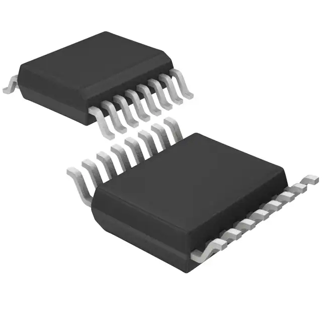


 工商网监
湘ICP备2023018690号
工商网监
湘ICP备2023018690号
