PT8A261/262
PIR Sensor Light Switch Controller
Features
•
•
•
•
•
•
•
•
•
•
•
•
•
•
General Description
2-stage operational amplifier as filter
Built-in noise rejection circuit
On-chip regulator
Override function
Synchronous with AC 220V/50Hz and 110V/60Hz
Pulse output (PT8A261) for TRIAC drive or
level output (PT8A262) for relay drive
CDS to enable/disable output
Adjustable output on time duration
ON/AUTO/OFF selectable by MODE pin
Auto-reset if the ZC signal disappears over 3
seconds
40 seconds warm-up
Quick check mode for initial installation
Operating voltage: 5V
Stand-by current: 80µA
The PT8A261 and PT8A262 are low power mixed signal
CMOS LSI designed for the automatic lamp control using
PIR sensor as motion detector.
With on chip noise filter and voltage regulator, the IC
provides stable operations throughout temperature
range. CDS input to disable day time operation is
desired.
Applications
• Energy saving auto-switch in Garden, kitchen,
bathroom, corridor, storage or yard
• Auto light in meeting room
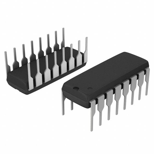
Ordering Information
Block Diagram
Pa r t N umbe r
Pa ck a ge
PT8A261PE/PT8A262PE
Lead free 16 - Pin PDIP
PT8A261WE/PT8A262WE
Lead free and Green
16 - Pin SO IC
PT8A261DE / PT8A262DE
Die Form
Note: Adding X suffix=Tape/Reel
OP2O
OP2N
OP2P
_
+
OP1N
latch circuit
Mode and CDS
control circuit
Voltage
divider
OP1O
OP1P
Comparator
Control
circuit
+
_
Output circuit
MODE
CDS
RELAY
(for 262 only)
TRIAC
(for 261 only)
Regulator
VEE
12-07-0007
OSCD
delay
oscillator
Delay
circuit
OSCS
System
oscillator
Counter
circuit
1
RST
Zero cross
debounce
ZC
PT0075-5
07/06/2012
�PT8A261/262
PIR Sensor Light Switch Controller
Pad Location
Pad Location of PT8A261DE
1470um
Die No.
CDS
ZC
OSCD
OSCS
TRIAC
GND
VCC
OP2O
1710um
MODE
VCC
OP2N
NC
OP2P
VEE
RST
OPIP OPIN OPIO
Pad Coordinate
Pad Name
X Coordinate
GND
570
TRIAC
570
OSCD
570
OSCS
570
ZC
-378.8
CDS
-30.1
MODE
570
VCC
-197.1
VCC
136.9
Note: Substrate is connected to GND
12-07-0007
Y Coordinate
Pad Name
X Coordinate
Y Coordinate
65.4
-101.6
399.4
232.4
689.2
-687.2
-435.6
-687.2
-687.2
NC
VEE
RST
OP1P
OP1N
OP1O
OP2P
OP2N
OP2O
570
-570
303.9
-44.8
-211.8
-570
-570
-570
-570
-268.6
232.4
-687.2
689.2
689.2
-435.6
-268.6
-101.6
65.4
2
PT0075-5
07/06/2012
�PT8A261/262
PIR Sensor Light Switch Controller
Pad Location of PT8A262DE
1470um
Die No.
CDS
ZC
OSCD
OSCS
RELAY
GND
VCC
OP2O
1710um
MODE
VCC
OP2N
NC
OP2P
VEE
RST
OPIP OPIN OPIO
Pad Coordinate
Pad Name
X Coordinate
GND
570
RELAY
570
OSCD
570
OSCS
570
ZC
-378.8
CDS
-30.1
MODE
570
VCC
-197.1
VCC
136.9
Note: Substrate is connected to GND
12-07-0007
Y Coordinate
Pad Name
X Coordinate
Y Coordinate
65.4
-101.6
399.4
232.4
689.2
-687.2
-435.6
-687.2
-687.2
NC
VEE
RST
OP1P
OP1N
OP1O
OP2P
OP2N
OP2O
570
-570
303.9
-44.8
-211.8
-570
-570
-570
-570
-268.6
232.4
-687.2
689.2
689.2
-435.6
-268.6
-101.6
65.4
3
PT0075-5
07/06/2012
�PT8A261/262
PIR Sensor Light Switch Controller
Pin Assignment
Figure 2
PT8A261P/PT8A261W
GND
TRIAC
OSCD
OSCS
ZC
CDS
MODE
VCC
1
2
3
4
5
6
7
8
16
15
14
13
12
11
10
9
PT8A262P/PT8A262W
OP2O
OP2N
OP2P
OP1O
OP1N
OP1P
RST
VEE
GND
RELAY
OSCD
OSCS
ZC
CDS
MODE
VCC
Top view
1
2
3
4
5
6
7
8
16
15
14
13
12
11
10
9
OP2O
OP2N
OP2P
OP1O
OP1N
OP1P
RST
VEE
Top view
Pin Description
Table 1
P in /Pa d
Na me
Descr ip t ion
Typ e
261
262
1
1
GND
2
RELAY
O
RELAY drive output through an external NPN transistor, active high
TRIAC
O
TRIAC drive two-pulse output, active negative pulse.
2
Ground Ground
3
3
OSCD
I/O
Output timing oscillator I/O, connected to an external RC to adjust output duration.
4
4
OSCS
I/O
System oscillator I/O, connected to an external RC to set the system frequency. The system
frequency = 16kHz for normal application.
5
5
ZC
I
Schmitt input for AC zero crossing detection.
6
6
CDS
I
Connected to a CDS voltage divider for daytime/night auto-detection. Low input to this pin
can disable PIR input. CDS is a schmitt trigger input with 5-second input debounce time.
7
7
MODE
I
Mode select, connecting to VCC- output always on, connection GND - output always off,
open - auto detection
8
8
VCC
Power
9
9
VEE
O
Internal voltage regulator output, 3.6V with respect to ground. Connected to the drain of
PIR sensor
10
10
RST
I
Chip reset input, active low, kept floating or connected an RC network
11
11
OP1P
I
Non-inverted input of first operational amplifier, connected directly to source of PIR sensor
12
12
OP1N
I
Inverted input of first operational amplifier
13
13
OP1O
O
Output of first operational amplifier
14
14
OP2P
I
Non-inverted input of second operational amplifier.
15
15
OP2N
I
Inverted input of second operational amplifier
16
16
OP2O
O
Output of second operational amplifier
12-07-0007
Power supply
4
PT0075-5
07/06/2012
�PT8A261/262
PIR Sensor Light Switch Controller
Functional Descriptions
OSCS and OSCD Pins
The PT8A261 and PT8A262 are CMOS LSI chips designed for
automatic PIR lamp control. They can operate in 2-wire configuration for triac applications or in 3-wire configuration for
relay applications.
OSCS is a system oscillator I/O pin connected to an external
RC to generate system frequency of 16kHz.
OSCD is an output timing oscillator I/O pin. It’s connected to
an external RC to obtain the desired turn-on duration by selecting various values of RC or using a variable resistor.FOSCD
is the frequency of OSCD pin, output timing can be caculated
as the formula: TD = 21504/FOSCD
The device consists of operational amplifiers, a comparator,
timer, a zero crossing detector, control circuit, a voltage regulator, a system oscillator, and an output timing oscillator.
CDS Input Circuit
The PIR sensor detects infrared power variations caused by
motion of a human body and transfer to a voltage variation. If
the PIR output voltage variation conforms to criteria, the lamp
is turned on for an adjustable duration. The PT8A261 (or 262)
offers three operating modes (ON, AUTO, OFF) which can be
set through a MODE pin. When the device is working in AUTO
mode, the user can override the mode to switch it to TEST
mode or manual ON mode, or return to the AUTO mode by
switching power switch.
CDS is a CMOS schmitt trigger input pin. It is used to distinguish between day time and night time. When the input voltage of CDS is high the PIR input is enabled, when CDS low the
PIR input disabled. The input disable-to-enable debounce
time is 5 seconds. Connect this pin to VCC when not using it.
The CDS input is ignored when the TRIAC or RELAY output
is active.
Figure 3. System Oscillator
Figure 4. Output Timing Oscillator
TD = 21504/FOSCD
RS
CS
RD
560K
OSCS PT8A261/
262
OSCD
CD
200P
Figure 5. CDS Input Circuit
Table 2. CDS Pin Function
VCC
Rp
Schmitt
Driver
CDS
CDS
PT8A261/
262
Control
CDS Circuit
C DS
St a t u s
PIR
L OW
Day Time
Disabled
HI GH
Night
Enabled
PT8A261/262
Figure 6. CDS Enable Debounce
CDS
< 5s
> 5s
PIREnable
12-07-0007
Disable
5
Enable
PT0075-5
07/06/2012
�PT8A261/262
PIR Sensor Light Switch Controller
vice can be toggled from ON to AUTO by switching the power
switch twice within 3 seconds again (override operation).
MODE
MODE is a tri-state input pin for operation mode selection.
See the following table 3.
If the chip is overridden to ON and there is no further override
operation, it will return to AUTO automatically after an internal preset ON time duration (8 hours).
Override Control: The term override refers to the change of
operating mode by switching the power switch twice within 3
seconds. When the chip is working in the AUTO mode (MODE
pin openned), the output is activated by a valid PIR trigger
signal and the output active duration is controlled by the OSCD
oscillation period. The lamp can be switched to ON from the
AUTO mode by either switching the MODE pin to VCC or
switching the power switch twice within 3 seconds. The de-
The override operation will cause the lamp flash (for TRIAC
version only). It will flash 3 times at 1Hz rate when changing
AUTO mode to other mode, and flash 3 times at 2Hz rate when
returning to AUTO mode. But no flash if mode is changed by
switching the MODE switch. See Figure 7 for override timing.
Table 3. Operation Modes by MODE Pin
MO DE
St a t u s
O p er a t ion
Mod e
Descr ip t ion
VCC
ON
Output is always ON: RELAY pin sends high level for relay driving; TRIAC pulse train output is
synchronized by ZC for triac driving.
GND
OFF
Output is always OFF: RELAY pin sends low level for relay driving; TRIAC pin sends high level
for triac driving.
Open
AUTO
Outputs remain in the OFF state until activated by a valid PIR trigger input signal. When working
in the AUTO mode, the device allows override control by switching the ZC signal.
Figure 7. Override Timing
Operating Mode
AUTO
flash
flash
flash
ON
AUTO
flash
ON
AUTO
8 hours
ZC
Flash is only for TRIAC version
Figure 8. RST Application Example
RST Pin
RST is used to reset the device. It is internal pull-high and
active low. The use of CRST can extend the power-on initial
time. If the RST pin is openned (without CRST), the initial
time is 40 seconds. See Figure 8.
VCC
REST
RST
CRST
GND
12-07-0007
6
PT0075-5
07/06/2012
�PT8A261/262
PIR Sensor Light Switch Controller
In case that the ZC signal disappears more than 3 seconds, the
chip will restart the initialization operation. However, the restart initial time is always 40 seconds and cannot be extended
by adding CRST to the RST pin as shown in Figure 6.
Power On Initial
The PIR signal amplifier requires a warm up period after poweron. The input should be disabled during this period.
Trigger
In the AUTO mode within the first 10 seconds of the initial
time the chip allows override control to enter the quickly install mode.After 40s of the initial time the chip allows override control between ON and AUTO. It will remain in the warm
up period if the total initial time has not elapsed after returning to AUTO.
The trigger timing is shown in Figure 9.
Retrigger -- If another signal is attained in trigger hold time,
the circuit will be retriggered, and the trigger hold time will be
restarted from this time.
Figure 9. Trigger Timing
RST
CDS
5s
Output
Enable
+trigger level
Comparator
Input
-trigger level
>24ms
Comparator
Output
0.34 seconds, and
- 2 triggers within 2 seconds with pulse duration of one > 0.16 seconds.
- The effective comparator output width is 24ms.(Fosc=16KHz)
2. The output duration is set by an external RC connected to the OSCD pin.
12-07-0007
7
PT0075-5
07/06/2012
�PT8A261/262
PIR Sensor Light Switch Controller
Maximum Ratings
(Above which the useful life may be impaired. For user guidelines, not tested)
Note:
Stresses greater than those listed under MAXIMUM
o
o
Storage Temperature ...................................................... -40 C to +125 C
RATINGS may cause permanent damage to the
Supply Voltage to Ground Potential (Inputs & VCC Only) .... -0.3 to +6.0V
device. This is a stress rating only and functional
Supply Voltage to Ground Potential (Outputs & D/O Only) -0.3 to +6.0V operation of the device at these or any other condiDC Input Voltage ................................................................ -0.3 to +6.0V tions above those indicated in the operational secDC Output Current ........................................................................ 20mA tions of this specification is not implied. Exposure
Power Dissipation ....................................................................... 500mW to absolute maximum rating conditions for extended periods may affect reliability.
Recommended Operation Conditions
Sym
Descr ip t ion
Min
Typ
Ma x
Un it s
VCC
Supply Voltage
4.75
5.0
6.0
V
VIH
Input HIGH Voltage (MODE,RST)
0.8VCC
-
-
V
VIL
Input LOW Voltage (MODE,RST)
-
-
0.2VCC
V
fSYS
System Oscillator Frequency
12.8
16
19.2
kHz
fDOSC
Delay Oscillator Frequency
12.8
16
19.2
kHz
TA
Operation Temperature
-25
25
70
O
C
DC Electrical Characteristics
Sym
Descr ip t ion
Test C on d it ion s
Min
Typ
Ma x
Un it s
IIH
Input high level leakage current(ZC,CDS)
VIH = 4.5V
-0.1
-
0.1
µΑ
IIL
Input low level leakage current(ZC,CDS)
VIL = 0.5V
-0.1
-
0.1
µΑ
IOH
Output Source Current (RELAY, TRIAC)
VOH = 4.5V
-6
-
-
mA
IOL
Output Sink Current (RELAY, TRIAC)
VOL = 0.5V
15
-
-
mA
VTH1
CDS Transfer High Voltage
3.0
3.2
3.6
V
VTL1
CDS Transfer Low Voltage
1.5
1.7
2.1
V
VTH2
ZC Transfer High Voltage
2.6
2.9
3.2
V
VTL2
ZC Transfer Low Voltage
1.0
1.4
1.6
V
VTH3
OSCS Transfer High Voltage
2.2
2.4
2.8
V
VTL3
OSCS Transfer Low Voltage
1.0
1.4
1.6
V
VTH4
OSCD Transfer High Voltage
2.2
2.4
2.8
V
VTL4
OSCD Transfer Low Voltage
0.4
0.6
0.8
V
Note: These specifications apply for VCC = 5.0V and -25OC ≤ TA ≤ 70OC, unless otherwise specified.
12-07-0007
8
PT0075-5
07/06/2012
�PT8A261/262
PIR Sensor Light Switch Controller
AC Electrical Characteristics
Voltage Regulator
Sym
Descr ip t ion
Test C on d it ion s
Min
Typ
Ma x
Un it s
VEE
Output Voltage
No load
3.2
3.6
4.0
VOP2P
Noninverting input of OP2
No load
1.6
1.8
2.0
∆VΟ
Line Regulation
4.5V ≤ VCC ≤ 5.5V, IL = 1mA
-
30
50
mV
∆VLDR
Load Regulation
VCC = 5V, 0.5mA ≤ IL ≤ 2mA
-
60
100
mV
IL
Regulator Output Current
VCC = 5V
4
-
-
mA
V
V
Operational Amplifier and Window Comparator
Sym
Descr ip t ion
Test C on d it ion s
Min
Typ
Ma x
Un it s
BW
3dB Bandwidth
-
10
-
-
kHz
VCC = 5V
1.9
2.05
2.2
V
VCC = 5V
1.4
1.55
1.7
V
VTH
VTL
12-07-0007
Windows Comparator Threshold
9
PT0075-5
07/06/2012
�PT8A261/262
PIR Sensor Light Switch Controller
Oscillator and ZC Input Pulse and Trigger Output Pulse
Min
Typ
Ma x
Un it s
Oscillator Frequency
12.8
16
19.2
kHz
tZR
ZC Pulse Rise Time
-
30
100
ns
tZF
ZC Pulse Fall Time
-
30
100
ns
tZP
ZC Pulse Period
15.1
20
22.2
ms
tZW
ZC Pulse Width
0.8
1
-
ms
tOR
TRIAC Pulse Rise Time
-
30
100
ns
tOF
TRIAC Pulse Fall Time
-
30
100
ns
tOP
TRIAC Pulse Period
6.6
10
11
ms
tOW
TRIAC Pulse Width
52
62.5
76
µs
Sym
Descr ip t ion
fOSC
Test C on d it ion s
VCC= 5V, RS = 560Ω,
CS = 200pF, see above fig 3
Figure 10. Timing Diagram
tZR
ZC
tZF
tZW
tZP
tOF
tOR
TRIAC
tOW
tOP
Power Dissipation
Sym
Descr ip t ion
Test C on d it ion s
Min
Typ
Ma x
Un it s
ICC
Power Supply Current
VCC = 5V, RS = 560kΩ ,CS=200P,
RD = 560kΩ , CD = 200P,
other input pins = GND, all
outputs float. see fig 3,4
-
80
100
µA
ICCQ
Quiescent Power Supply Current
VCC = 5V, All Input Pins = GND,
all outputs float.
-
60
80
µA
12-07-0007
10
PT0075-5
07/06/2012
�12-07-0007
11
AC
110V~230V
TRIAC
Q1
LAMP
20~100 W
ON/OFF
OVERRIDE
SW1
1
2
3
R1
20K
68/2W
R14
104
C8
1N4007
D2
0.68U/350V
C10
C11
1N40 07
D5
1M
R9
470UF/16V
R9 200K
1N4007
D3
D4
6.2 V
D1
1N4148
R10
R2
2.4M
CDS
R13
R 8 560K
1M
R7
MODE
SW 2
OF F
AUTO
ON
C3
201
C7
3900P
VCC
MODE
CDS
ZC
OSCS
OSCD
TRIAC
GND
100UF/16V
C1
8
7
6
5
4
3
2
1
E
9
10
11
12
13
14
15
16
C4
100UF/16V
VE
RST
OP1P
OP1N
OP1O
OP2P
OP2N
OP2O
PT8A261
1M
203
C5
SD6222
D
S
G
10UF/16V
C9
R6
C6
56K
C13
203
R3
C2
203
22UF/16V
22UF/
16V
C12
R12
22K
1M
R4
R5
22K
PT8A261/262
PIR Sensor Light Switch Controller
Typical Application Circuits
Figure 11. Two-Wire Application Circuit of PT8A261
PT0075-5
07/06/2012
�12-07-0007
12
ON/OFF
OVERRIDE
1M
R8
1N4007
D5
Q1
C5
1N4148
D4
100UF/35V
D6
1N4007
24V D3
24V D2
68/2W
R6
C13
3.3nf/63V
K1
D1
IN4148
R13
3.3K
CDS
R1
2.4M
R7
R9 560K
R10 1M
R14 4.7K
R12
9014
201
C3
SW2
MODE
C6
3900P
D7
5.1V
ON
SW1
AC 110V~230V
C11
0.68U/350V
LAMP
20~100W
VCC
MODE
CDS
ZC
OSCS
OSCD
RELAY
GND
470UF/16V
C9
8
7
6
5
4
3
2
1
14
9
C4
100UF/16V
VEE
RST 10
OP1P
11
OP1N 12
OP1O 13
OP2P
OP2N 15
OP2O 16
PT8A262
SD6222
D
S
G
C6
C13
203
56K
R3
C2
203
22UF/16V
10UF/16V
C10
203
C5
1M
R6
22UF/16V
C12
R12
22K
R4
1M
R5
22K
PT8A261/262
PIR Sensor Light Switch Controller
Figure 12. Three-Wire Application Circuit of PT8A262
AUTO
OFF
PT0075-5
07/06/2012
�PT8A261/262
PIR Sensor Light Switch Controller
Mechanical Information
P(DIP-16)
12-07-0007
13
PT0075-5
07/06/2012
�PT8A261/262
PIR Sensor Light Switch Controller
W(SOIC-16)
Pericom Semiconductor Corparation 1-800-435-2336 www.pericom.com
Pericom Technology Incorporation reserves the right to make changes to its products or specifications at any time, without notice, in order to
improve design or performance and to supply the best possible product. Pericom Technology does not assume any responsibility for use of any
circuitry described other than the circuitry embodied in Pericom Technology product. The company makes no representations that circuitry
described herein is free from patent infringement or other rights, of Pericom.
12-07-0007
14
PT0075-5
07/06/2012
�


 工商网监
湘ICP备2023018690号
工商网监
湘ICP备2023018690号
