SUPPLY VOLTAGE
MONITOR
ZSM380
ISSUE 2 – JANUARY 2003
DEVICE DESCRIPTION
FEATURES
The ZSM380 is a three terminal under
v o l t a g e m o n i t or c ir c ui t fo r u s e i n
microprocessor systems. The threshold
voltage of the device has been set to 3.8 volts
making it ideal for 5 volt circuits.
•
•
•
•
•
•
•
Included in the device is a precise voltage
reference and a comparator with built in
hysteresis to prevent erratic operation. The
ZSM380 features an open collector output
capable of sinking at least l0mA which only
requires a single external resistor to
interface to following circuits.
•
•
Operation of the device is guaranteed from
one volt upwards, from this level to the
device threshold voltage the output is held
low providing a power on reset function.
Should the supply voltage, once established,
at any time drop below the threshold level
then the output again will pull low.
SOT223 and TO92 packages
Power on reset generator
Automatic reset generation
Low standby current
Guaranteed operation from 1 volt
Wide supply voltage range
Internal clamp diode to discharge
delay capacitor
3.8 volt threshold for 5 volt logic
20mV hysteresis prevents erratic operation
APPLICATIONS
•
•
•
•
•
•
The device is available in a TO92 package for
through hole applications as well as SOT223
for surface mount requirements.
SCHEMATIC DIAGRAM
4-349
Microprocessor systems
Computers
Computer peripherals
Instrumentation
Automotive
Battery powered equipment
�ZSM380
ABSOLUTE MAXIMUM RATING
Input Supply Voltage
Offstate Output Voltage
Onstate Output
Sink Current(Note 1)
Clamp Diode
Forward Current(Note 1)
Operating Junction
Temperature
Operating Temperature
Storage Temperature
-1 to 10V
10V
Power Dissipation
TO92
SOT223
780mW
2W(Note 2)
Internally limited
100mA
150°C
-40 to 85°C
-55 to 150°C
TEST CONDITIONS
(Tamb=25°C for typical values, Tamb=-40 to 85°C for min/max values (Note3))
COMPARATOR
MIN
TYP.
MAX.
PARAMETER
SYMBOL
Threshold Voltage
High state output (Vcc increasing)
UNITS
V IH
3.7
3.81
3.9
V
Threshold Voltage
Low state output (Vcc decreasing)
V IL
3.7
3.79
3.9
V
Hysteresis
VH
0.01
0.02
0.05
V
(Vcc=3.3V, Isink=8.0mA)
0.46
1.0
V
(Vcc=3.3V, Isink=2.0mA)
0.15
0.4
V
0.25
V
27
60
mA
0.02
0.5
µA
1.2
1.5
V
OUPUT
Output sink saturation:
V OL
(Vcc=1.0V, Isink=0.1mA)
Onstate output sink current
(Vcc , Output=3.3V)
Isink
Offstate output leakage current
(Vcc , Output=5V)
Ioh
Clamp diode forward voltage
(If=10mA)
Vf
Propagation delay
(Vin 5V to 3.3V, Rl=10k, Tamb=25°C)
Td
10
0.6
µs
3
TOTAL DEVICE
Operating input voltage range
V cc
Quiescent input current (Vcc=5V)
Iq
1.0 to 6.5
V
140
200
µA
Note:
1. Maximum package power dissipation must be observed.
2. Maximum power dissipation for the SOT223 package is calculated assuming that the device is
mounted on a PCB measuring 2 inches square.
3. Low duty cycle pulse techniques are used during test to maintain junction temperatures as
close to ambient as possible.
4-350
�ZSM380
TYPICAL CHARACTERISTICS
500
10
400
8
Rl =10K
Ta =25°C
Output Voltage (V)
Input Current (µA)
85°C
25°C
-40°C
300
200
6
4
2
100
0
0
0
2
4
6
8
10
0
2
Input Voltage (V)
Input Current vs. Input Voltage
4
Input Voltage
(V)
6
8
10
Output Voltage vs. Input Voltage
50
Rl =10K
Vin=3.3V
5
30
3.3
25°C
�
85°C
4
-40°C
20
10
�
2
Vout
(V)
Sink Current (mA)
Vin
(V)
40
0
0
0
0.4
0.8
1.2
1.6
0
2.0
2
4
6
Time (µs)
Output Saturation Voltage (V)
Output I(sink) vs. Output V(sat)
Reset Delay Time
3.82
50
Vin=0V
Upper Threshold
3.81
30
Threshold Voltage (V)
Forward Current (mA)
40
85°C
25°C
-40°C
20
10
0.4
0.8
1.2
1.6
3.79
Lower Threshold
3.78
3.77
-40
0
0
3.80
2.0
-20
0
20
40
60
80
100
Forward Voltage (V)
Temperature ( °C)
Clamp Diode I(forward) vs. Voltage
Threshold Voltage vs. Temperature
4-351
�ZSM380
TIMING DIAGRAM
Vcc
Threshold
Voltage
1V
Output
Output
Undefined
Output
Undefined
APPLICATION CIRCUIT
Note 4:
A time delayed reset can be accomplished with the additional Cd.
æ
T DY = RCd ln ç
ç
1
ç
è
−
1
ö
V TH (mpu ) ÷÷
V in
÷
ø
TDY =Time (Seconds)
VTH =Microprocessor Reset Threshold
Vin =Power Supply Voltage
4-352
�ZSM380
CONNECTION DIAGRAMS
SOT223
Package Suffix – G
TO92
Top View –
Pin 4 floating or connected to pin 2
Package Suffix – C
Bottom View
ORDERING INFORMATION
Part Number
Package
Part Mark
ZSM380G
SOT223
ZSM380
ZSM380C
TO92
ZSM380
4-353
�PRODUCT AND INFORMATION DISCLAIMER
This publication is issued to provide outline information only which (unless agreed by the
Company in writing) may not be used, applied or reproduced for any purposes or form part of any
order or contract or be regarded as representation relating to the products or services concerned.
The company reserves the right to alter without notice the specification, design, price or
conditions of supply of any product or service.
Some changes to earlier published data may have been made, data presented in this hand book
supersedes all previous specifications. The information contained in this publication has been
carefully checked and is considered to be accurate, but no responsibility is assumed for any
inaccuracies.
Zetex makes no warranty, representation or guarantee regarding the suitability of the products
and circuits in this publication for any given purpose; nor does Zetex assume any liability arising
from the use or application of any of these products or circuits and specifically disclaims any and
all consequential and incidental damages.
Zetex products are specifically not authorised for use as critical components in life support
devices or systems without the express written approval of the Managing Director of Zetex plc.
As used herein a. Life support devices or systems are devices or systems which
(1) are intended to implant into the body, or
(2) support or sustain life and whose failure to perform when properly used in accordance
with instructions for use provided in the labelling can be reasonably expected to result in
significant injury to the user.
b. A critical component is any component in a life support device or system whose failure to
perform can be reasonably expected to cause the failure of the life support device or to affect its
safety or effectiveness.
E. & O. E.
”all rights reserved“
© Zetex plc 2002
Americas
Asia Pacific
Zetex GmbH
Streitfeldstraße 19
D-81673 München
Zetex Inc
700 Veterans Memorial Hwy
Hauppauge, NY11788
Germany
Telefon: (49) 89 45 49 49 0
Fax: (49) 89 45 49 49 49
europe.sales@zetex.com
USA
Telephone: (631) 360 2222
Fax: (631) 360 8222
usa.sales@zetex.com
Zetex (Asia) Ltd
3701-04 Metroplaza, Tower 1
Hing Fong Road
Kwai Fong
Hong Kong
Telephone: (852) 26100 611
Fax: (852) 24250 494
asia.sales@zetex.com
Europe
Zetex plc
Fields New Road
Chadderton
Oldham, OL9 8NP
United Kingdom
Telephone (44) 161 622 4422
Fax: (44) 161 622 4420
uk.sales@zetex.com
These offices are supported by agents and distributors in major countries world-wide.
This publication is issued to provide outline information only which (unless agreed by the Company in writing) may not be used, applied or reproduced
for any purpose or form part of any order or contract or be regarded as a representation relating to the products or services concerned. The Company
reserves the right to alter without notice the specification, design, price or conditions of supply of any product or service.
For the latest product information, log on to
www.zetex.com
�
很抱歉,暂时无法提供与“ZSM380CSTOB”相匹配的价格&库存,您可以联系我们找货
免费人工找货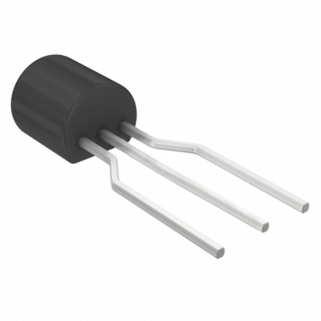


 工商网监
湘ICP备2023018690号
工商网监
湘ICP备2023018690号
