ZXCW6100S28
Winner of the (British) Electronics Industry Design Award
for the “Best Use of Technology”
24 BIT STEREO DIRECT DRIVE DIGITAL AUDIO AMPLIFIER
SUMMARY
The ZXCW6100S28 is part of the Acoustar™ range of new generation
digital audio power devices from Zetex. It has a level of performance not
offered by any other solution and with minimal components forms a
complete audio interface from digital audio data to the loudspeaker.
FEATURES
• Typical solution performance
•
•
•
•
•
•
THD+N (1W into 4⍀) 0.05%
Dynamic range 101dB
Noise floor -110dB
•
•
•
•
•
•
•
•
•
•
24 Bit Conversion
All common digital audio standards supported
All sampling rates up to 192kHz supported
Direct Drive PWM output
Noise Shaper stability up to full modulation
Effective PWM frequency up to 1MHz
Digital Volume, Mute, Bass and Treble control
NOVALOAD™ for clipping control
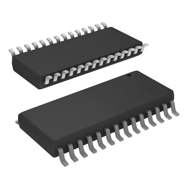
28 pin SSOP package
768 times over sampling (single speed mode)
APPLICATIONS
16 times digital filtering (single speed mode)
•
•
•
•
•
Digital De-emphasis 32,44.1,48kHz
ATAPI mux/mute CD-ROM standard
3 wire SPI control interface
ZTA filter system
5.1 Integrated DVD amplifiers
Home theatre systems
Mini Hi-fi
Automotive audio
PC audio
Soft Mute, digital silence
ISSUE 2 - FEBRUARY 2004
1
SEMICONDUCTORS
�ZXCW6100S28
DESCRIPTION
The ZXCW6100 is part of a new generation of stereo
digital audio power amplifier devices. The device
offers a move forward to a new level of performance
not offered by another solution. The ZXCW6100
operates in direct drive mode and can be selected to be
with or without dead time.
The device is controlled via a 3 wire SPI (Serial
Peripheral Interface) interface from the host system
controller. Device function control is achieved by
writing an 8-bit control and 64 bit data string to internal
registers within the ZXCW6100 chip. The SPI interface
is bi-directional, allowing the configuration to be read
back as required.
Exceptional performance can be achieved with the
ZXCW6100 device in direct drive mode, the dynamic
range is 101dB, the noise floor sits at –110dB and when
driving 1W into 4⍀ THD+N is 0.05%. The device
supports all common digital audio input formats.
Multiple devices can easily be configured together by
using the SPI enable of each ZXCW6100. This means
that in 5.1 surround sound systems, for example, three
ZXCW6100 devices can be configured together.
The device provides direct drive Pulse Width
Modulation (PWM) 2 channel stereo outputs which, via
a FET drive interface with an H Bridge output stage,
forms a full solution to Digital Power Amplification.
Reference designs are available for the solutions with
typical power levels up to 60W.
Sampling frequencies up to 192kHz are fully
supported, dependant on which sampling frequency is
selected then the device can operate in single, dual or
quad speed modes. In single speed mode, then the
popular 44.1kHz sampling from audio CDs is
oversampled up to 768 times. This results in a master
clock speed of 33MHz. Digital de-emphasis is also
supported as well as mixing and muting according to
the ATAPI CD-ROM standard.
The ZXCW6100 device operates from a 3.3V supply
with an operating temperature range from -40⬚C to
+85⬚C. The device is supplied in a 28 pin SSOP package.
Other key features include user definable digital
control of Volume, Mute, Bass & Treble. The device
also features Zetex unique overload management
system NOVALOAD™. NOVALOAD™ can operate in
several ways to modify either volume, tone or both
with user definable attack and decay rates. There is a
hard mute available as well as a mute with digital
silence, whereby the output stage is set to the
quiescent state.
ISSUE 2 - FEBRUARY 2004
SEMICONDUCTORS
2
�ZXCW6100S28
ABSOLUTE MAXIMUM RATINGS
Supply voltage (VCC)
Digital input current
Digital output current
Digital input voltage
Digital output voltage
Package power dissipation
Storage temperature
-0.3 to 4.0V
+/-20mA
+/-20mA
-0.3 to VCC + 0.3V
-0.3 to VCC + 0.3V
1.4W
-55 to 125°C
Note: The Absolute Maximum Ratings indicate levels where permanent damage to the device may occur. Functional operation is not guaranteed
under theses conditions. Operation at any of the absolute maximum conditions for extended periods may adversely affect the long term reliability
of the device.
PACKAGE CHARACTERISTICS
Thermal resistance
⍜JA (junction to ambient)
49°C/W
OPERATING CONDITIONS
Symbol
Parameter
V CC
Supply voltage
TO
Operating temperature range
Conditions
Min
Typ
Max
3
3.3
3.6
V
85
⬚C
-40
Unit
DC ELECTRICAL CHARACTERISTICS
TEST CONDITIONS (Unless otherwise stated): VCC = 3.3V, TAMB = 25⬚C
SUPPLY CHARACTERISTICS
Symbol
Parameter
Conditions
Min
Typ
Max
Unit
IS
Static Supply current
All clocks & data static
I DD
Operational supply current
112
10.5
144
A
mA
PD
Dissipation
380
475
mW
Max
Unit
DIGITAL INPUT CHARACTERISTICS
Symbol
Parameter
Conditions
V IH
High level input voltage
V IL
Low level input voltage
V OUT ⱖ V OH(min) or
V OUT ⱕ V OUT(max)
I IN
Input current
V IN = 0V or V CC
IC
Input capacitance
Min
Typ
2
V CC +0.3 V
-0.3
0.8
+/-0.5
4.7
V
µA
pF
DIGITAL INPUT WITH ACTIVE PULL-UP CHARACTERISTICS
Symbol
Parameter
Conditions
V IH
High level input voltage
V IL
Low level input voltage
V OUT ⱖ V OH(min) or
V OUT ⱕ V OUT(max)
I IL
Low level Input current
V IN = 0V
I IH
High level Input current
IC
Input capacitance
Min
Typ
2
Max
Unit
V CC +0.3 V
-0.3
-53
4.7
0.8
V
-70
µA
0.5
µA
pF
ISSUE 2 - FEBRUARY 2004
3
SEMICONDUCTORS
�ZXCW6100S28
DIGITAL INPUT WITH ACTIVE PULL-DOWN CHARACTERISTICS
Symbol
Parameter
Conditions
V IH
High level input voltage
V IL
Low level input voltage
V OUT ⱖ V OH(min) or
V OUT ⱕ V OUT(max)
Min
Typ
I IL
Low level Input current
V IN = V CC
I IH
High level Input current
60
IC
Input capacitance
4.7
2
Max
Unit
V CC +0.3 V
-0.3
0.8
V
-0.5
µA
75
µA
pF
DIGITAL OUTPUT CHARACTERISTICS
Symbol
Parameter
Conditions
Min
V OH
High level output voltage
2.4
V OL
Low level output voltage
V CC = 3V, or I OH = -12mA
V CC = 3V, or I OL = 12mA
Min
Typ
Max
Unit
V
0.4
V
DIGITAL IO CHARACTERISTICS
Symbol
Parameter
Conditions
V IH
High level input voltage
V IL
Low level input voltage
V OUT ⱖ V OH(min) or
V OUT ⱕ V OUT(max)
I IN
Input current
V IN = 0V or V CC
IC
Input capacitance
V OH
High level output voltage
V OL
Low level output voltage
Typ
2
Max
-0.3
0.8
+/-0.5
4.71
V CC = 3V, or I OH = -8mA
V CC = 3V, or I OL = 8mA
Unit
V CC +0.3 V
V
µA
pF
2.4
V
0.4
V
AC ELECTRICAL CHARACTERISTICS
TEST CONDITIONS (Unless otherwise stated): VCC = 3.3V, TAMB = 25⬚C
MASTER CLOCK
Symbol
Parameter
M CK
Clock frequency
M MS
Mark to space ratio
Conditions
Min
40:60
Typ
Max
Unit
33.8688
40
MHz
60:40
%
ISSUE 2 - FEBRUARY 2004
SEMICONDUCTORS
4
�ZXCW6100S28
SWITCHING CHARACTERISTICS: SPI INTERFACE - WRITE
Symbol
Parameter
S CK
SPI-CK clock frequency
t spids
SPI-DA set-up time
0.5
ns
t spidh
SPI-DA hold time
0.1
ns
t spies
SPI-EN hold time
0.7
ns
t spieh
SPI-EN hold time
0.1
ns
t spiemh
SPI-EN minimum high time
Note:
1
Conditions
Min
Typ
Max
Unit
M CK /8
40
MHz
M-CK 1
3
M-CK = Master Clock Cycles.
SWITCHING CHARACTERISTICS: SPI INTERFACE - READ
Symbol
Parameter
Conditions
Min
Typ
Max
S CK
SPI-CK clock frequency
t spids
SPI-DA set-up time
t spidh
SPI-DA Data hold time
t spidov
time to valid SPI-DA data out
t spies
SPI-EN hold time
0.7
ns
t spieh
SPI-EN hold time
0.1
ns
t spiemh
SPI-EN minimum high time
Note:
1
40
Unit
0.5
0.1
Load capacitance (C L ) = 50pf
ns
2.1
3
MHz
ns
ns
M-CK 1
M-CK = Master Clock Cycles.
ISSUE 2 - FEBRUARY 2004
5
SEMICONDUCTORS
�ZXCW6100S28
SWITCHING CHARACTERISTICS: AUDIO INPUT DATA
Symbol
Parameter
B CK
BIT-CK clock frequency
t sds
S-DATA set-up time
1
M-CK 1
t sph
S-DATA hold time
1
M-CK 1
t wcks
WORD-CLK set-up time
1
M-CK 1
t wckh
WORD-CLK hold time
1
M-CK 1
Note:
1
Conditions
Min
Typ
Max
Unit
M CK /8
40
MHz
M-CK = Master Clock Cycles.
MASTER CLOCK TO PWM OUTPUT CHARACTERISTICS
Symbol
Parameter
t mckop
M-CK to PWM output delay
t opskew
PWM output to output skew
250
ps
t spdt
PWM output to deadband
output time
14.8
ns 2
Note:
2
Conditions
Min
Typ
3.0
Max
Unit
ns
This translates to the low period of the Master Clock (M-CI) cycles.
ISSUE 2 - FEBRUARY 2004
SEMICONDUCTORS
6
�ZXCW6100S28
TYPICAL CHARACTERISTICS
10
5
0
100Hz Boost
Flat
Response
200Hz Boost
200Hz Cut
-5
100Hz Cut
-10
50Hz Cut
-15
10
15
50Hz Boost
Amplitude (dB)
Amplitude (dB)
15
100
1k
12kHz Boost
10
5
8kHz Boost
0
-5
4kHz Cut
8kHz Cut
-10
12kHz Cut
-15
10k 20k
Flat
Response
4kHz Boost
10
100
1k
Frequency (Hz)
Frequency (Hz)
Bass Response
Treble Response
10k 20k
ISSUE 2 - FEBRUARY 2004
7
SEMICONDUCTORS
�ZXCW6100S28
PINOUT DIAGRAM
PIN DESCRIPTIONS
Pin
Name
Type
Description
1
SPI-EN
LVTTL IP
SPI interface enable, active low
2
SPI-DA
LVTTL I/O
SPI data
3
SPI-CK
LVTTL IP
SPI clock
4
CSLO
LVTTL IP+PU Connect to logic Gnd
5
CSL1
LVTTL IP+PU Connect to logic Gnd
6
VCC-LOGIC
Core logic supply voltage, 3.3V
7
GND-LOGIC
Core logic ground
8
WORD-CK
LVTTL IP
Digital audio word clock, matches to system sampling rate
9
BIT-CK
LVTTL IP
Digital audio bit clock
10
S-DATA
LVTTL IP
Serial digital audio data input
11
MUTE
LVTTL IP+PU Mute enable, active low
12
VCC-LOGIC
13
GND-LOGIC
14
M-CK
LVTTL IP
System master clock
15
OP4-R
LVTTL OP
Right channel PWM drive output, see applications section
16
OP3-R
LVTTL OP
17
GND-R
Right channel PWM drive output ground
18
VCC-R
Right channel PWM drive output supply, 3.3V
19
OP2-R
LVTTL OP
20
OP1-R
LVTTL OP
Right channel PWM drive output, see applications section
21
OP4-L
LVTTL OP
Left channel PWM drive output, see applications section
22
OP3-L
LVTTL OP
23
GND-L
24
VCC-L
25
OP2-L
LVTTL OP
Left channel PWM drive output, see applications section
26
OP1-L
LVTTL OP
Left channel PWM drive output, see applications section
27
MODE0
LVTTL IP+PU Mode select, direct drive with or without dead time
28
MODE1
LVTTL IP+PD Connect to Gnd
Note
Core Logic supply, 3.3V
Core Logic ground
Right channel PWM drive output, see applications section
Right channel PWM drive output, see applications section
Left channel PWM drive output, see applications section
Left channel PWM drive output ground
Left channel PWM drive output supply, 3.3V
+PU = with Pull-up Device
+PD = with Pull-down Device
ISSUE 2 - FEBRUARY 2004
SEMICONDUCTORS
8
�ZXCW6100S28
BLOCK DIAGRAM
FUNCTIONAL DEVICE DESCRIPTION
The ZXCW6100 device is an integrated stereo digital
amplifier. It takes in digital audio data, in any of the
common digital audio formats, processes it and
delivers a PWM direct drive left and right channel
output. The direct drive PWM output can be used to
drive full bridge tied load output stages configured to
deliver typical power in the range 10W to 50W and
above.
Format converter
The format converter ensures the device is compatible
with all the normal digital input standards. The
standards supported are:
24 bit I2S
Left justify 24 bit
SPI Interface
Right justify 16 bit
Right justify 24 bit
The device is controlled by a 3 wire SPI interface. The 8
bit control and 64 bit data words directed through the
SPI interface are used to control all the functions of the
ZXCW6100 device:
Chip address
The audio data for left and right channels is transmitted
in the high and low periods of the word clock
depending on the format chosen. The first received
audio data is held until the corresponding channel data
is received. The left and right channels data are then
processed in parallel. The word clock represents the
sampling rate of the audio data input, also referred to
as Fs.
Volume/Mute
Bass/Treble
De-emphasis
Volume
Digital volume control is achieved through the SPI port.
Volume can be set anywhere in the range of -94.5dB to
+25dB in 0.5dB steps. A code is included in the volume
register to enable a soft mute function to be achieved,
this set to -95dB.
NOVALOAD™
Audio data format
ATAPI CD-ROM standard
PWM drive outputs
A digital silence function is also available, this is
selected by activating the auto low power mode. In this
case, if no serial digital data is detected for a period of
4096 word clocks then the output stage is switched off.
In this mode minimum EMC signature is experienced.
Auto power low
Speed mode
The SPI interface is bi-directional such that the
appropriate programmed configuration and data can
be read back if required.
ISSUE 2 - FEBRUARY 2004
9
SEMICONDUCTORS
�ZXCW6100S28
Bass
ZTA filters
The bass control can be set to a selection of corner
frequencies:
The ZTA filters use the proprietary ZTA algorithm to
perform up to 48 times digital filtering. The speed
mode of the device selects the oversampling
performed:
50Hz
100Hz
1200Hz
Single speed
Dual speed
Quad speed
16 times
8 times
4 times
These corner frequencies are stated for a nominal
44.1kHz sampling frequency. If the sampling frequency
is altered then the corner frequency is automatically
adjusted. Once selected then the bass control can be
set to either cut or boost with gain from 0dB up to 15dB
in 1dB steps.
In addition to providing state of the art out of band
noise performance, the ZTA filter gives superior
transient resolution, which improves sound stage
imaging, timing, focus and bass definition.
Treble
Noise shaper & PWM drive
The treble control can be set to a selection of corner
frequencies:
The noise shaper effectively offers continuous
feedback to the system. It enables removal of any dead
time distortion and enables the drive to the PWM FET
switching. Switching distortions are also removed by
the noise shaper.
4kHz
8kHz
12kHz
These corner frequencies are stated for a nominal
44.1kHz sampling frequency. If the sampling frequency
is altered then the corner frequency is automatically
adjusted. Once selected then the treble control can be
set to either cut or boost with gain from 0dB up to 15dB
in 1dB steps.
Master clock
Essential to the performance of the system is the
provision of a low jitter clock to the ZXCW6100 device,
a jitter of less than +/-1ns is required. As well as low
jitter the master clock needs to be a consistent mark to
space ratio. This master clock is generated from the
external audio system, consistency needs to be better
than 3ns with a 33MHz master clock.
The relationship between the master clock and the
word clock provided with the audio data input
determines the device speed and oversampling rate for
the ZTA filters and the Noise shaper/PWM drive. The
master clock is a nominal 33.8688MHz for a 44.1kHz fs
(sampling rate) with 768 times oversampling.
Sampling Rates
The ZXCW6100 device supports a wide range of
sampling rates depending on the media being played.
Typically as follows:
Single speed
Dual speed
Quad speed
32kHz, 44.1kHz, 48kHz
88.2kHz, 96kHz
176.4kHz, 192kHz
The PWM output converts the noise shaper output into
four PWM drive lines per channel. These output lines,
suitably buffered, drive a full MOSFET H bridge. The
output is configured as a bridge tied load. Each of the
four output lines drives N and P channel MOSFET pairs.
The effective PWM frequency is 1MHz, significantly
faster than alternative solutions. This high frequency
allows for greater resolution and enables lower noise
and distortion figures to be achieved. The PWM output
can be utilised either with or without dead time
enabled.
Two different modulation schemes are available,
known as HPWM and RPWM, these two schemes have
different strengths that the user can take advantage of
as they are selectable through the SPI interface.
Accompanying the two PWM schemes is the ability to
select one of two switching frequencies to help attain
the best performance from the PWM scheme and
output stage combination.
HPWM is a conventional digital PWM strategy that is to
be found in current applications. The frequency of
operation is 1.058MHz, derived from 24 times the
44.1kHz sampling frequency.
HPWM provides a lower level of overall RF noise in the
AM band with that noise concentrated on multiples of
the switching frequency. With very careful OP stage
design it is capable of the best measured dynamic
range.
ISSUE 2 - FEBRUARY 2004
SEMICONDUCTORS
10
�ZXCW6100S28
RPWM is a proprietary PWM scheme that applies
different data to both sides of a conventional H bridge
output stage. The primary purpose of this is to
maximise the resolution of the internal noise shaper.
This doubles the noise shaper resolution. The other
advantage of RPWM is that the FET switching
frequency is halved. RPM therefore can have two
speeds of 529kHz and 1.058MHz. This lower speed
does not reduce the noise shaper performance.
The nature of RPWM also ensures that it is less
susceptible to correlated jitter on the master clock
resulting in a better signal to noise ratio with jittery
clocks.
The recommended mode of operation for new users is
HPWM.
Chip select
It is possible to cascade several ZXCW6100 devices for
multi-channel applications. Each chip is accessed
using the appropriate SPI enable line. Valid data for the
individual ZXCW6100 is clocked in during SPI enable
low periods. SPI data and clock can be common. A
separate enable line per device is required.
Mute
A hard mute facility is provided for the device when
used in direct drive mode. Active low, this control will
shut off the output drive. Once released, the output will
remain disabled for approximately 0.5 seconds.
Additionally this facility can be used to provide thermal
and current overload protection.
Mode
The direct drive ZXCW6100 device can be operated in
different modes. In the configuration provided, the
device can operate with or without dead time
d e p e n d i ng on t he s el ec t i on of out p u t d r i v e
characteristics. The direct drive ZXCW6100 device can
be selected though external input pins to operate with
or without dead time. It is recommended to run the
device without dead time.
Full details about the use of these modes is available in
the associated Application document. Contact your
nearest Zetex office for full details.
Supplies
The device is provided with several power supply
connections. A nominal 3.3 volt supply is required with
the supply pairs being de-coupled separately and as
close to the device as possible.
NOVALOAD™
The NOVALOAD™ system provides a mechanism for
overload control. It can operate in several different
ways as it acts to back off the gain of the volume or bass
blocks. Once activated there are two modes of
operation available for the user to select. With the
NOVALOAD™ Mode register bit NOVLM = 1 any
overload in the volume circuit block will result in the
gain of the volume block being reduced and if any
overload takes place in the bass circuit block then the
volume is again reduced keeping the bass boost
unaffected. With the NOVLM = 0 any overload in the
volume block will result in the gain of the volume block
being reduced, however, if any overload is present due
to bass boost the bass boost is removed completely.
When no bass clipping has occurred for a period of
time greater than that set by the limiter release rate
register (but not greater than two times that period) the
bass boost is fully restored to its previous level as
determined by the bass gain register.
The rate at which the volume is reduced in response to
clipping can be programmed through the SPI interface.
The gain reduces by 0.5dB over a selected number of
word clock periods. Typically this will be set to 0.5dB in
4 word clocks. Once the overload condition is removed
then the gain is released to increase again. This is also
programmable as 0.5dB per selected number of word
clocks. Typically this will be set to 0.5dB per 16 word
clock periods.
The release rate coming out of NOVALOAD™ is critical
to a good sound. Typically 2 seconds is suggested for
pop and rock, 4 to 8 seconds for classical.
De-emphasis
De-emphasis is activated when older audio recordings
are used in the system. These will have used
pre-emphasis to achieve noise reduction. The
de-emphasis frequency response curve is selected
versus the system sampling rate. De-emphasis only
applies in single speed mode.
ISSUE 2 - FEBRUARY 2004
11
SEMICONDUCTORS
�ZXCW6100S28
PIN FUNCTIONAL DESCRIPTIONS
SPI interface
Pins SPI-EN, SPI-DA, SPI-CK form the SPI interface. The
enable, SPI-EN, is active low. Data is transmitted on
SPI-DA as a 72 bit word, there are 8 control bits and 64
data bits, SPI-CK provides the clock for the SPI
interface. The function of the control and data bits is
detailed in the Register Description section. The SPI
interface is also bi-directional with the read/write
function set in the first 8 control bits.
In write mode (figure 1) a full 72 bits is sent from the
host controller consisting of the 8 preamble control bits
with the R/W bit set low and the 64 SPI data bits. The
SPI-EN signal must be held low, enabled, for all 72
clocks and data bits as a validity check is run on the
incoming data string and any string not 72 bit long is
rejected. It is recommended to perform a read back of
the SPI data registers to validate the receipt of the
correct instruction.
Data can be sent to SPI interface using two methods burst mode or continuos mode. In burst mode data will
be sent as a single 72 bit SPI data word accompanied by
72 SPI-CK clock bits. This data would be sent as and
when operating parameters are required to be
changed.
In continuous mode the SPI-CK clock will run
continuously with the SPI-DA data being resent
regardless of whether operating parameters are
required to be changed or not. The only requirement
for this mode, or for burst mode, as regard the
frequency of SPI update is that the SPI-EN enable line is
returned high for a minimum of 3 M-CK master clock
cycles between SPI data words.
The SPI interface can operate asynchronously to the
M-CK master clock and to any other data inputs. It can
run up to a maximum of 40 MHz however, it is expected
that one eighth the M-CK clock frequency would be
normal for most requirements.
In read mode (figure 2) the host controller sends the
first 8 preamble control bits with the R/W bit set high.
The SPI-DA pin of the ZXCW6100 device changes state
from being an input to being an output on the falling
edge following the R/W bit. The device then reads out
the data from the internal SPI register onto the SPI-DA
wire.
SPI Interface - Write Mode (figure 1)
SPI Interface - Read Mode (figure 2)
ISSUE 2 - FEBRUARY 2004
SEMICONDUCTORS
12
�ZXCW6100S28
Audio input data
The audio input utilises three pins, WORD-CK, BIT-CK
and S-DATA. The diagrams below indicate the
appropriate timing diagrams for the 4 possible input
formats.
Left Justify 24 bit
24 bit I2S Compatible
Right Justify 16 or 24 bit
ISSUE 2 - FEBRUARY 2004
13
SEMICONDUCTORS
�ZXCW6100S28
Mute
SPI REGISTER SUMMARY
Mute is enabled with the MUTE pin. Mute is active low.
The following indicates the general structure of the 72
bit SPI word used for control and data.
Master clock
Control
The system master clock is applied to pin M-CK
SPI preamble:
Output drive
Output drive is provided on 8 pins, 4 each for left and
right. For each channel the pins are OP1 to OP4 then L
or R. OP1 and OP2 as a pair drive the gates of an N & P
channel MOSFET pair through a gate drive buffer that
includes dead time control. OP3 and OP4 drive a similar
pair. These pairs in turn drive a BTL (bridge tied load)
loudspeaker – see the Typical Applications Diagram for
details. Timing diagrams are shown in the AC
Characteristics section.
Operating mode
MODE0 pin
MODE1 pin
Direct drive no
dead time
0
0
Direct drive
with dead time
1
0
ca1 ca0 1 00011
ca1 ca0 1 00010
read
write
Bits ca1 and ca0 should be set low. The next 4 bits are a
silicon reference to the ZXCW6100 part number. The
other two bits determine if the SPI interface is in read or
write modes.
Mode (dead/no dead time)
MODE0 and MODE1 are used to set the operating
mode of the ZXCW6100 device. There are two modes
available, direct drive with and without dead time.
Without dead time the output stage on and off
switching to the N and P channel MOSFETs occurs at
the same time. The user can then design any dead time
or cross conduction into the output stage as required
by the characteristics of the MOSFET being used.
When dead time is selected a delay is introduced
between the N and P channel MOSFET switching such
that the active MOSFET is switched off before the
inactive MOSFET is switched on. This is particularly
useful where MOSFETs have a slow turn off time and
might otherwise give a large amount of cross
conduction in the N and P channel MOSFET pair.
Dead time is a function of the master clock frequency
and is effectively a half the master clock rate. For the
nominal 33MHz master clock, dead time is therefore
approximately 15ns.
Whilst this digital dead time is available it is
recommended for most applications that shorter
periods of dead time are used by including dead time
control within the FET drive buffer circuit.
ISSUE 2 - FEBRUARY 2004
SEMICONDUCTORS
14
�ZXCW6100S28
SPI bi-directional interface register
The interface control register defines the functionality of the device. It is a 64 bit register. Bit 64 is read as the MSB,
bit 0 is the LSB, MSB stated first. The default setting is 0 except where stated.
Bit No.
Function
0
volume left
Bit
Identifier
Comments/Example
vl0
vl8.............vl0
1
vl1
2
vl2
011111110 is 0dB
3
vl3
100110000 is +25 dB
4
vl4
001000001 is -94.5dB
5
vl5
001000000 = soft mute
6
vl6
011111010 is default power up, -2 dB
7
vl7
See volume code tables
8
vl8
9
volume right
vr0
vr8.............vr0
10
vr1
11
vr2
011111110 is 0dB
12
vr3
100110000 is +25 dB
13
vr4
001000001 is -94.5dB
14
vr5
001000000 = soft mute
15
vr6
011111010 is default power up, -2 dB
16
vr7
See volume code tables
17
vr8
18
bass boost
bb
19
bass gain
bg0
1 = bass boost, 0 = bass cut
20
bg1
bg = 1111 gives +/- 15dB
21
bg2
bg = 0000 gives +/- 0dB
22
bg3
See bass code table
bf0
bf = 00: 50Hz, bf = 01: 100 Hz, bf = 10: 1.2kHz
23
bass freq
24
bf1
25
treble boost
tb
26
treble gain
tg0
1 = treble boost, 0 = treble cut
27
tg1
tg = 1111 gives +/- 15dB
28
tg2
tg = 0000 gives +/- 0dB
29
tg3
See treble code table
tf0
tf = 00: 4kHz, tf = 01: 8kHz, tf = 10: 12kHz
30
treble freq
31
tf1
ISSUE 2 - FEBRUARY 2004
15
SEMICONDUCTORS
�ZXCW6100S28
SPI bi-directional interface register (cont)
Bit No.
Function
Bit
Identifier
Comments/Example
32
50/15s standard
de0
de = 00: none, de = 01: 44.1kHz
33
de-emphasis
de1
de = 10: 32kHz, de = 11: 48kHz
34
novaload
novl
0 = disable, 1 = enable
35
novaload mode
novlm
0 adjust vol if vol clips, remove bass if bass clips
1 adjust vol if vol clips, adjust vol if bass clips
36
dc dither
dcadd
1= dc dither on
37
limiter
lar0
adjusts how quickly the volume is reduced during a clip
38
attack rate
lar1
see attack code table
lar2
default 001, 0.5 ms per -3dB
39
40
limiter
lrr0
41
release rate
lrr1
adjusts how quickly the volume is increased after a clip
42
lrr2
see release code table
43
lrr3
default 1010, 2 sec per +3dB
dif0
dif = 00: I 2 S, dif = 01: left justified,
dif1
dif = 10: right just 16 bit, dif = 11: right just 24 bit.
44
digital interface
45
46
ATAPI mix
ATI0
47
ATI1
Hard mute, mono and channel switch
48
ATI2
see ATAPI select tables
49
ATI3
1001 default
50
H-bridge on
hbon
hbon = 0: bridge off, hbon = 1 bridge on
in direct drive mode, default=0
51
P-channel
peer0
52
compensation
peer1
P error default: 10000
53
peer2
P-channel switching compensation
54
peer3
Valid range: 00000-10000
55
peer4
56
N-channel
neer0
57
compensation
neer1
N error default: 00000
58
neer2
N channel switching compensation
59
neer3
Valid range: 00000-10000
60
neer4
61
auto low power
al
auto low power mode
al = 0: disabled, al = 1: enabled
62
set speed & pwm
hspd
Low speed = 0
High speed = 1
63
combination
hpwm
hpwm = 1
rpwm = 0
ISSUE 2 - FEBRUARY 2004
SEMICONDUCTORS
16
�ZXCW6100S28
SPI REGISTER DETAILED DESCRIPTION
Volume
Treble
The volume register increments digitally in 0.5dB
steps. The volume range is from -94.5db to +25dB. The
final used code in the sequence it termed a soft mute
and sets the volume to -95dB. The code sequence
applies equally to left and right volume controls. The
bit numbers for the volume controls are 0 to 8 for the
left channel and 9 to 17 for the right.
The treble register increments digitally in steps of 1dB.
The range is from 0dB to +/-15dB depending on
whether the treble control is set to cut or boost (bit25).
The bit numbers for the treble level control are 26 to 29.
Bit25: boost=1, cut=0
Code examples in the sequence follow:
The control of the volume should not jump directly
from one level to the next but should pass through all
0.5dB steps between the two required levels.
Code examples in the sequence follow:
0000
0001
=
=
+/-0dB
+/-1dB
1110
1111
=
=
+/-14dB
+/-15dB
100110000
100101111
100101110
=
=
=
25dB
24.5dB
24dB
The treble corner frequency is selected by bits 30 & 31.
00
=
4kHz
01
=
8kHz
10
=
12kHz
011111111
011111110
011111101
=
=
=
0.5dB
0dB
-0.5dB
50/15 s Standard De-emphasis
011111010
=
-2dB
(default and start up)
001000010
=
-94dB
001000001
=
-94.5dB
001000000
=
-95dB
(-95dB is the soft mute)
The ZXCW6100 incorporates a standard 50/15s digital
de-emphasis filter. De-emphasis is applicable in single
speed mode only.
Bits 32 and 33 match to sampling frequencies as below:
00
01
10
11
Bass
=
=
=
=
no de-emphasis
44.1kHz
32kHz
48kHz
The bass register increments digitally in steps of 1dB.
The range is from 0dB to +/-15dB depending on
whether the bass control is set to cut or boost (bit18).
The bit numbers for the bass level control are 19 to 22.
Bit18: boost=1, cut=0
Code examples in the sequence follow:
0000
0001
=
=
+/-0dB
+/-1dB
1110
1111
=
=
+/-14dB
+/-15dB
The bass corner frequency is selected by bits 23 and 24.
00
=
50Hz
01
=
100Hz
10
=
200Hz
ISSUE 2 - FEBRUARY 2004
17
SEMICONDUCTORS
�ZXCW6100S28
DC Dither
NOVALOAD™ limiter release rate
A function is provided to help eliminate small signal
digital zero point switching distortion by the addition of
a small DC voltage. This is intended to move the signal
away from the DAC zero to prevent the distortion that is
sometimes discernible when the DAC switches around
zero.
The limiter release rate is governed by bits 40 to 43. The
code chosen sets the number of word clock periods to
reduce the gain by 0.5dB. The number of word clock
periods doubles per digital increment
DC Dither would be required when using the
recommended HPWM mode. If using RPWM DC dither
would not normally be set, however, the requirement
is application dependant and full details on use are
available in the associated Application document.
Contact your nearest Zetex office for full details.
Bit 36: 0 = DC dither off, 1 = DC dither on
Code examples in the sequence follow:
0000
0001
0010
=
=
=
16 word clock periods per 0.5dB
32 word clock periods per 0.5dB
64 word clock periods per 0.5dB
1110
1111
=
=
262144 word clock periods per 0.5dB
524288 word clock periods per 0.5dB
Digital interface select
The default condition is 1010 which is 16384 word clock
periods.
Bits 44 and 45 select the digital interface standard
required as below:
ATAPI
00
01
10
11
The ATAPI CD-ROM standard for mixing and muting is
supported by bits 46 to 49. The following logic table
defines how the left and right channels are affected by
the codes set on these bits:
24 bit I2S
Left justify 24 or 32 bit
Right justify 16 bit
Right justify 24 bit
ATI3
ATI2
ATI1
ATI0
L channel
R channel
0
0
0
0
MUTE
MUTE
0
0
0
1
MUTE
R
0
0
1
0
MUTE
L
0
0
1
1
MUTE
{(L+R)/2}
Bit 35: 0 = remove bass control if bass clips,
1 = adjust volume control if bass clips
0
1
0
0
R
MUTE
0
1
0
1
R
R
NOVALOAD™ limiter attack rate
0
1
1
0
R
L
0
1
1
1
R
{(L+R)/2}
1
0
0
0
L
MUTE
1
0
0
1
L
R
1
0
1
0
L
L
1
0
1
1
L
{(L+R)/2}
1
1
0
0
{(L+R)/2}
MUTE
1
1
0
1
{(L+R)/2}
R
1
1
1
0
{(L+R)/2}
L
1
1
1
1
{(L+R)/2}
{(L+R)/2}
NOVALOAD™
NOVALOAD™ is selected using bits 34 and 35 as
below:
Bit 34: 0 = NOVALOAD™ off, 1 = NOVALOAD™ on
The limiter attack rate is governed by bits 36 to 39. The
code chosen sets the number of word clock periods to
reduce the gain by 0.5dB. The number of word clock
periods quadruples per digital increment.
Code sequence follow:
000
001
010
011
100
101
110
111
=
=
=
=
=
=
=
=
1 word clock period per 0.5dB
4 word clock periods per 0.5dB
16 word clock periods per 0.5dB
64 word clock periods per 0.5dB
256 word clock periods per 0.5dB
1024 word clock periods per 0.5dB
4096 word clock periods per 0.5dB
16384 word clock periods per 0.5dB
The default setting is 1001 which is left channel = L,
right channel = R
The default condition is 0010 which is 4 word clock
periods.
ISSUE 2 - FEBRUARY 2004
SEMICONDUCTORS
18
�ZXCW6100S28
H bridge on
Bit 50 is used to enable the output drive to the H bridge,
this is used to control the power up sequence for the
system ensuring a safe power on:
Bit50: 0 = bridge off, 1 = bridge on
The default condition is output bridge off.
NEER & PEER FET Compensation
NEER and PEER provide compensation for fixed
switching errors within the OP FET’s. For the majority
of applications, NEER and PEER should be left set to the
default values. In order to further optimise the output
stage, for NEER use the values in the range from 00000
(default) to 01000 and for PEER use values in range
from 01000 to 10000 (default).
Auto low power
If activated then the digital silence feature is available.
Bit 61 controls the enable for auto low power:
Bit61: 0 = disabled, 1 = enable
Set pwm and speed combination
The two bits bit 62 (hspd) and bit 63 (hpwm) are used to
set up the speed and pwm methodology respectively.
Zetex recommend the use of HPWM. Full details about
the use of these modes will be available in the
associated Application document. Contact your
nearest Zetex office for full details.
Bit 62:
Bit 63:
0 = low speed
0 = RPWM
1 = high speed
1 = HPWM
The resultant operating modes are shown in the
following table:
hspd
hpwm Operating mode
0
0
RPWM at 500kHz
1
0
RPWM at 1MHz
0
1
HPWM 1
1
Note: recommended mode of operation
ISSUE 2 - FEBRUARY 2004
19
SEMICONDUCTORS
�ZXCW6100S28
TYPICAL CONNECTION DIAGRAM
The following shows a typical connection diagram for the output circuit of one channel of the ZXCW6100 device.
For dedicated Applications Notes please contact your nearest Zetex office.
TYPICAL PERFORMANCE CHARACTERISTICS
Parameter
Conditions
THD+N
HPWM 1W
Min
Typ
0.05
Max
Unit
%
Dynamic range
101
dB
Noise floor
-110
dB
ISSUE 2 - FEBRUARY 2004
SEMICONDUCTORS
20
�ZXCW6100S28
ISSUE 2 - FEBRUARY 2004
21
SEMICONDUCTORS
�ZXCW6100S28
ISSUE 2 - FEBRUARY 2004
SEMICONDUCTORS
22
�ZXCW6100S28
ISSUE 2 - FEBRUARY 2004
23
SEMICONDUCTORS
�ZXCW6100S28
PACKAGE OUTLINE
MILLIMETRES
MIN.
MAX.
A
1.70
2.00
A1
0.05
0.15
A2
1.65
1.85
D
9.90
10.50
E
7.40
8.20
E1
5.00
5.60
L
0.55
0.95
e
0.65 BSC
b
0.22
0.38
c
0.09
0.25
Comforms to JEDEC MO-187 VARIATION BA
ORDERING INFORMATION
DEVICE
ZXCW6100S28
PART MARKING
Zetex
Acoustar™
ZXCW6100
© Zetex plc 2002
Americas
Asia Pacific
Zetex GmbH
Streitfeldstraße 19
D-81673 München
Zetex Inc
700 Veterans Memorial Hwy
Hauppauge, NY11788
Germany
Telefon: (49) 89 45 49 49 0
Fax: (49) 89 45 49 49 49
europe.sales@zetex.com
USA
Telephone: (631) 360 2222
Fax: (631) 360 8222
usa.sales@zetex.com
Zetex (Asia) Ltd
3701-04 Metroplaza, Tower 1
Hing Fong Road
Kwai Fong
Hong Kong
Telephone: (852) 26100 611
Fax: (852) 24250 494
asia.sales@zetex.com
Europe
Zetex plc
Fields New Road
Chadderton
Oldham, OL9 8NP
United Kingdom
Telephone (44) 161 622 4422
Fax: (44) 161 622 4420
uk.sales@zetex.com
These offices are supported by agents and distributors in major countries world-wide.
This publication is issued to provide outline information only which (unless agreed by the Company in writing) may not be used, applied or reproduced
for any purpose or form part of any order or contract or be regarded as a representation relating to the products or services concerned. The Company
reserves the right to alter without notice the specification, design, price or conditions of supply of any product or service.
For the latest product information, log on to
www.zetex.com
ISSUE 2 - FEBRUARY 2004
SEMICONDUCTORS
24
�


 工商网监
湘ICP备2023018690号
工商网监
湘ICP备2023018690号
