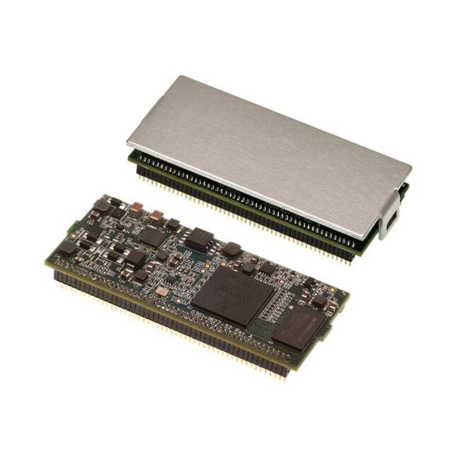
Powerline Modules
500Mbps Modules
The Single In-line Package (SIP) module is an IEEE1901 and
HomePlug AV based MAC/PHY/AFE Powerline Communications
(PLC) transceiver/modem.
The Module provides an integrated solution for Powerline
communications. The “Black Box” design requires no external
software and only a few external components to create a working
solution. Operate as a PHY or MAC is selectable via Pull up/down
resistor.
Communication is possible over any 2 wire system DC/AC or Dry
wire.
Key Features & Benefits
Based on Qualcomm Atheros AR7410/AR1500 chipset
Industrial Temperature Range -40°C – +85°C
Supports IEEE1901 HomePlug® AV Standard with data rates of
500Mbps
RGMII (0804-5000⬜50) or MII (0804-5000⬜51) (Host & PHY)
interface
Supports 4096/1024/256/64/16/8-QAM, QPSK, BPSK and
ROBO modulation schemes
128-bit AES Link Encryption with key management for secure
power line communications
Windowed OFDM with noise mitigation based on patented
line synchronization techniques improves data integrity in
noisy conditions
Dynamic channel adaptation and channel estimation
maximizes throughput in harsh channel conditions
Horizontal mounting configuration using standard 1.27mm
pin header (50 way)
Integrates core components necessary to add HomePlug AV
functionality to any embedded system at low cost
Designed to meet Class A conducted emissions EMC
standards for industrial applications
0804-5000⬜51 offers a MII interface and is compatible with
the existing 0804-5000-18/24 Modules
Models
Part Number
Temp Range
Interface
Market
0804-5000A50
-40°C – +85°C Including Heatsink
RGMII
US
0804-5000A51
-40°C – +85°C Including Heatsink
MII (0804-5000-18/24 compatible)
US
0804-5000E50
-40°C – +85°C Including Heatsink
RGMII
EU
0804-5000E51
-40°C – +85°C Including Heatsink
MII (0804-5000-18/24 compatible)
EU
Bel Modules
28 Turkey Court, Turkey Mill, Ashford Road
Maidstone ME14 5PP UK
+44 1622 757 395
techhelp@belf.com
belfuse.com
© 2017 Bel Power Solutions, Inc.
Rev E
[1]
�Powerline Modules
500Mbps Module
Module Block Diagram
GPIO
LEDs
AND
CONFIG
RGMII
MII
TX
DAC
M
P
A
H
C
Y
BPF
PLC
COUPLER
ADC
BPF
RX
AR1500
ZERO CROSS
DETECTOR
AR7410
RESET
SYS CLK
FLASH
PLL
RAM
3.3V
DC
DC/DC
CLOCK
1.26V 2.5V 11.2V
* Dotted line signifies Modules External connectivity.
System Block Diagram
POWER
AC Mains /
DC or Dry wire
RESET
RGMII/MII
PLC
COUPLER
PHY DEVICE
POWERLINE
MODULE
MDIO
OR
MAC
CONTROLLER
ZERRO CROSS
DETECTOR
PHY UTILITY
* AC only
GPIO
The block diagram presents the Powerline module in a typical environment.
techhelp@belf.com
belfuse.com
[2]
�Powerline Modules
500Mbps Module
Module Interface
Module connectivity is provided via a 50 way 1.27mm pitch gold pin header.
Pin Number
Pin Name
MII
Type
Description
RGMII
1
VDD
PWR
+3.3V
2
VSS
PWR
Ground
3
VDD
PWR
+3.3V
4
VSS
PWR
Ground
5
VNET_IO
PWR
+2.5V / +3.3V
6
TXRX+
I/O
Differential TXRX signal, connects to coupling transformer
7
TXRX-
I/O
Differential TXRX signal, connects to coupling transformer
8
VSS
PWR
Ground
RESERVED
[1]
-
Reserved pin
10
RESERVED
[1]
-
Reserved pin
11
RESET#
I
Resets all IC logic when low
12
GPIO0
I/O
Strap: ENET_SEL[0]
13
GPIO1
I/O
Strap: ENET_SEL[1]; Push-button: Simple connect
14
GPIO2
I/O
Strap: ANEN; Push-button: Factory default
15
RESERVED [1]
-
Reserved pin
16
GPIO4
I/O
Strap: SPEED_SEL[0]
17
GPIO5
I/O
Strap: MD_A3
18
GPIO6
I/O
Strap: CFG_SEL
19
GPIO7
I/O
Strap: MD_A4
20
GPIO8
I/O
Strap: MP_SEL; LED: Powerline Tx/Rx Link
21
GPIO3
I/O
Strap: ISODEF; LED: Ethernet Tx/Rx Link
22
GPIO10
I/O
Strap: BM_SEL
23
GPIO11
I/O
Strap: SPEED_SEL[1]; LED: Power
24
ZC_IN
I/O
Zero-cross detection signal
25
MDIO
I/O
Management Data Interface Data Line
26
MDC
9
OMAC/IPHY
Management Data Interface Clock Line
RESERVED
[1]
-
Reserved pin
28
RESERVED
[1]
-
Reserved pin
29
VSS
PWR
Ground
30
MRX_D0
RD0
IMAC/OPHY
MII / RGMII: Receive Data Bits (MAC)
31
MRX_D1
RD1
IMAC/OPHY
MII / RGMII: Receive Data Bits (MAC)
32
MRX_D2
RD2
IMAC/OPHY
MII / RGMII: Receive Data Bits (MAC)
33
MRX_D3
RD3
IMAC/OPHY
MII / RGMII: Receive Data Bits (MAC)
34
COL
RESERVED [2]
IMAC/OPHY
MII: Collision Detected
35
MRX_CLK
RXC
IMAC/OPHY
MII / RGMII: Receive Clock (MAC)
27
techhelp@belf.com
belfuse.com
[3]
�Powerline Modules
500Mbps Module
Pin Number
Pin Name
MII
Type
Description
PWR
Ground
RGMII
36
VSS
37
MRX_ERR
RESERVED [2]
IMAC/OPHY
MII: Receive Error (MAC)
38
MRX_DV
RX_CTL
IMAC/OPHY
MII: Receive Data Valid (MAC)
RGMII: Receive control signal (MAC)
39
MTX_D0
TD0
OMAC/IPHY
MII / RGMII: Transmit Data Bits (MAC)
40
MTX_D1
TD1
OMAC/IPHY
MII / RGMII: Transmit Data Bits (MAC)
41
MTX_D2
TD2
OMAC/IPHY
MII / RGMII: Transmit Data Bits (MAC)
42
MTX_D3
TD3
OMAC/IPHY
MII / RGMII: Transmit Data Bits (MAC)
IMAC/OPHY
MII: Carrier Sense
MII: Transmit Clock (MAC)
RGMII: Transmit Clock (MAC)
43
CRS
RESERVED
[2]
44
MTX_CLK
TXC
MII:
IMAC/OPHY
RGMII: OMAC/IPHY
45
MTX_EN
TX_CTL
OMAC/IPHY
MII: Transmit Enable (MAC)
RGMII: Transmit Control Signal (MAC)
46
VSS
PWR
Ground
47
PHY_RST#
O
Reset Ethernet PHY
48
VSS
PWR
Ground
49
PHY_CLK
O
Strap: DUPLEX; 25MHz Clock for Ethernet PHY
50
VSS
PWR
Ground
[1] Leave reserved pins disconnected
[2] Add pull down 10kΩ resistor
Ethernet interface
The Ethernet interface can be configured in MAC or PHY mode and depending on the module model either MII or RGMII
protocols are supported.
MAC or PHY mode
RGMII (0804-5000⬜50) or MII (0804-5000⬜51) protocol
In MAC mode, the SIP is configured to be an Ethernet MAC and to communicate to an external Ethernet PHY device. This
configuration is typical in an Ethernet Wall Adapter application. In PHY mode, the SIP is configured to be a Physical Medium
Dependent (PMD) or PHY controller. In this configuration, an external MAC controls the SIP; this configuration is typical in
an embedded application, such as a set-top box. Regardless of which mode is used, the SIP can be configured to use one of
below protocols:
MII (100 Mbps max) Complies with 802.3(u)
RGMII (1000 Mbps max) Supports RGMII v1.3 with internal 2ns delays
The MAC and PHY configurations support 10 and 100 Mbps in half and full-duplex, and 1000 Mbps in full duplex mode only.
When the RGMII interface is used, regardless of the speed, only full-duplex is supported. Flow control is supported in
half-duplex using “back-pressure” preamble assertion, and using pause packets in full-duplex mode. The Ethernet interface
includes the management data interface for MAC and PHY controller functions. The Ethernet MAC module implements a
standard Ethernet MAC function. The Ethernet MAC will be connected to an external Ethernet PHY function. The MAC
configuration provides bridging between Ethernet and PLC. The PHY configuration emulates Ethernet PHY functionality and
provides PLC connectivity to devices designed to communicate over an Ethernet physical network.
The Ethernet interface has separate transmit and receive packet buffering. When operating as a MAC the transmit FIFO is 2
KB and the receive FIFO is 16 KB. When operating as a PHY controller, the transmit FIFO is 16 KB and the receive FIFO is 2
KB.
techhelp@belf.com
belfuse.com
[4]
�Powerline Modules
500Mbps Module
MII Bus Signals
Pin
Number
Pin Name
30
31
32
33
MRX_D0
MRX_D1
MRX_D2
MRX_D3
34
35
37
COL
MRX_CLK
MRX_ERR
38
MRX_DV
39
40
41
42
MTX_D0
MTX_D1
MTX_D2
MTX_D3
43
44
45
CRS
MTX_CLK
MTX_EN
I/O
MAC Mode
I
I
I
I
I
O
I
I
O
Description
PHY Mode
O
Transmit Data Bits. The PHY controller drives MRX_D[3:0] and the MAC core
receives MRX_D[3:0]. MRX_D[3:0] transition synchronously with respect to
MRX_CLK. For each MRX_CLK period in which MRX_DV is asserted,
MRX_D[3:0] is valid. MRX_D0 is the least-significant bit. The PHY controller tristates MRX_D[3:0] in isolate mode.
O
Collision Detected. The PHY controller asserts COL when it detects a collision
on the medium. COL remains asserted while the collision condition persists.
COL signal transitions are not synchronous to either the MTX_CLK or the
MRX_CLK. The MAC core ignores the COL signal when operating in the fullduplex mode. The PHY controller tri-states COL in isolate mode.
O
Receive Clock. MRX_CLK is a continuous clock that provides the timing
reference for the transfer of the MRX_DV and MRX_D[3:0] signals from the PHY
controller to the MAC core. The PHY controller sources MRX_CLK. MRX_CLK
frequency is equal to 25% of the data rate of the received signal on the
Ethernet cable. The PHY controller tri-states MRX_CLK in isolate mode.
O
Receive Error. The PHY controller asserts MRX_ERR high for one or more
MRX_CLK periods to indicate to the MAC core that an error (a coding error or
any error that the PHY is capable of detecting that is otherwise undetectable by
the MAC) was detected somewhere in the current frame. MRX_ERR transitions
synchronously with respect to MRX_CLK. While MRX_DV is de-asserted,
MRX_ERR has no effect on the MAC core. The PHY controller tri-states
MRX_ERR in isolate mode.
O
Receive Data Valid. The PHY controller asserts MRX_DV to indicate to the MAC
core that it is presenting the recovered and decoded data bits on MRX_D[3:0]
and that the data on MRX_D[3:0] is synchronous to MRX_CLK. MRX_DV
transitions synchronously with respect to MRX_CLK. MRX_DV remains asserted
continuously from the first recovered nibble of the frame through the final
recovered nibble, and is de-asserted prior to the first MRX_CLK that follows the
final nibble. The PHY controller tri-states MRX_DV in isolate mode.
I
Transmit Data Bits. The MAC core drives MTX_D[3:0] and the PHY controller
receives MTX_D[3:0]. MTX_D[3:0] transitions synchronously with respect to
MTX_CLK. For each MTX_CLK period in which MTX_EN is asserted, MTX_D[3:0]
is valid. MTX_D0 is the least-significant bit. The PHY controller ignores
MTX_D[3:0] in isolate mode.
O
Carrier Sense. The PHY controller asserts CRS when either transmit or receive
medium is non-idle. The PHY de-asserts CRS when both transmit and receive
medium are idle. The PHY must ensure that CRS remains asserted throughout
the duration of a collision condition. The transitions on the CRS signal are not
synchronous to either the MTX_CLK or the MRX_CLK. The PHY controller tristates CRS in isolate mode.
O
Transmit Clock. MTX_CLK is a continuous clock that provides a timing
reference for the transfer of the MTX_EN and MTX_D[3:0] signals from the
MAC core to the PHY controller. The PHY controller sources MTX_CLK. The
operating frequency of MTX_CLK is 25 MHz when operating at 100 Mbps and
2.5 MHz when operating at 10 Mbps. The PHY controller tri-states MTX_CLK in
isolate mode.
I
Transmit Enable. A high assertion on MTX_EN indicates that the MAC core is
presenting nibbles to the PHY controller for transmission. The SIP MAC core
asserts MTX_EN with the first nibble of the preamble and keeps MTX_EN
asserted while all nibbles to be transmitted are presented to the MII. MTX_EN
is de-asserted prior to the first MTX_CLK following the final nibble of the frame.
MTX_EN transitions synchronously with respect to MTX_CLK. The PHY
controller ignores MTX_EN in isolate mode.
techhelp@belf.com
belfuse.com
[5]
�Powerline Modules
500Mbps Module
RGMII Bus Signals
Pin Number
Pin Name
I/O
MAC Mode
PHY Mode
Description
30
31
32
33
35
RD0
RD1
RD2
RD3
RXC
I
O
Transmit Data Bits. The PHY controller drives RD[3:0] and the MAC core
receives RD[3:0]. The Signals contains the bits 3:0 on rising and 7:4 on falling
edges of the RXC. The PHY controller tri-states RD[3:0] in isolate mode.
I
O
38
RX_CTL
I
O
39
40
41
42
44
TD0
TD1
TD2
TD3
TXC
O
I
Receive Clock. RXC is a continuous double data rate (DDR) clock that
provides the timing reference for the transfer of the RX_CTL and RD[3:0]
signals from the PHY controller to the MAC core. RXC frequency is equal to
25% of the data rate of the received signal on the Ethernet cable in 10/100
Mbps mode, and 12.5% of the data rate of the received signal on the
Ethernet cable in 1000 Mbps mode. The PHY controller tri-states RXC in
isolate mode.
Receive Data Valid. RX_CTL is driven by the PHY controller. Contains the
RXDV on rising and RXERR on falling edges of the RXC. The PHY controller
tri-states RX_CTL in isolate mode.
Transmit Data Bits. The MAC core drives TD[3:0] and the PHY controller
receives TD[3:0]. The Signals contains the bits 3:0 on rising and 7:4 on falling
edges of the TXC. The PHY controller tri-states RD[3:0] in isolate mode.
O
I
45
TX_CTL
O
I
Transmit Clock. TXC is a continuous double data rate (DDR) clock that
provides a timing reference for the transfer of the TX_CTL and TD[3:0]
signals from the MAC core to the PHY controller. The operating frequency of
TXC is 125 MHz when operating at 1000 Mbps, 25 MHz when operating at
100 Mbps and 2.5 MHz when operating at 10 Mbps. The PHY controller tristates TXC in isolate mode.
Transmit Control Signal. TX_CTL is drives by the MAC core. Contains the
TXEN on rising and a logical derivative of TXEN and TXERR on falling edges of
the TXC. The PHY controller tri-states TX_CTL in isolate mode.
Management Data Interface (MDI)
The Ethernet interface has a two-wire bi-directional serial Management Data Interface (MDI). This interface provides access
to the status and control registers in the Ethernet PHY logic.
Pin Number
Pin Name
I/O
MAC Mode
PHY Mode
Description
25
MDIO
I/O
I/O
MII Management Data In/Out. This is the data input signal from the PHY
controller. The PHY drives the Read Data synchronously with respect to the
MDC clock during the read cycles. This is also the data output signal from the
MAC core that drives the control information during the Read/Write cycles to
the PHY controller. The MAC core drives the MDO signal synchronously with
respect to the MDC.
26
MDC
O
I/O
MII Management Data Clock. The MAC core sources MDC as the timing
reference for transfer of information on the MDI/MDO signals. MDC signal
has no maximum high or low times. MDC minimum high and low times are
160 ns each, and the minimum period for MDC is 400 ns.
techhelp@belf.com
belfuse.com
[6]
�Powerline Modules
500Mbps Module
Ethernet Options
The MP_SEL strap is used to specify which mode PHY or MAC the module operates in. The encoding of this signal is shown
in the following table:
MP_SEL
Mode
0
PHY mode
1
MAC mode
ENET_SEL[1:0]
MII/RGMII
00
10/100/1000 RGMII No Rx Clk Delay
(0804-5000⬜50 ONLY)
01
10/100/1000 RGMII 2ns Rx Clk Delay
(0804-5000⬜50 ONLY)
10
Not Used
11
10/100 MII
(0804-5000⬜51 ONLY)
In PHY mode, there are 5 additional configuration straps that are unique to this mode of operation:
SPEED_SEL[1:0]
MII/RGMII Speed
MD_A[4:3]
Management Address
00
10Mbps
00
0x00
01
100Mbps
01
0x08
10
1000Mbps (0804-5000⬜50 ONLY)
10
0x10
11
Reserved
11
0x18
ISODEF
Isolation
ANEN
Negotiation Mode
0
Normal Operation
0
Auto-Negotiate Disabled
1
Isolated
1
Auto-Negotiate Enabled
DUPLEX
MII Duplex
0
Half Duplex
1
Full Duplex
techhelp@belf.com
belfuse.com
[7]
�Powerline Modules
500Mbps Module
RGMII and MII Interface Timing Parameters
MII Tx Bus (MTX) and Rx Bus (MRX) Timing
Parameter
tCLKp
tCLKhi
tCLKlo
tOV
tSU
tH
Min
Max
Units
CLK Period (100 Mb/s, 10 Mb/s)
40/400
-
ns
CLK High Time (100 Mb/s, 10 Mb/s)
14/140
26/260
ns
CLK Low Time (100 Mb/s, 10 Mb/s)
14/140
26/260
ns
Output Valid Time All MTX Signals
10
28
ns
Input Set Up Time All MRX Signals
10
-
ns
Input Hold Time All MRX Signals
10
-
ns
Min
Max
Units
MDC Period (100 Mb/s, 10 Mb/s)
400
-
ns
MDC High Time (100 Mb/s, 10 Mb/s)
150
-
ns
MDC Low Time (100 Mb/s, 10 Mb/s)
150
-
ns
Output Valid MDIO
0
300
ns
Input Set Up Time MDIO
10
-
ns
Input Hold Time MDIO
10
-
ns
Management Data Interface Clock (MDC) and Data (MDIO) Timing
Parameter
tMDCp
tMDChi
tMDCIo
tMOV
tMSU
tMH
Table 1 MII Timing Specification MAC Mode
techhelp@belf.com
belfuse.com
[8]
�Powerline Modules
500Mbps Module
MII Tx Bus (MTX) and Rx Bus (MRX) Timing
Parameter
tCLKp
tCLKhi
tCLKlo
tOV
tOH
tSU
tH
Min
Max
Units
CLK Period (100 Mb/s, 10 Mb/s)
40/400
-
ns
CLK High Time (100 Mb/s, 10 Mb/s)
14/140
26/260
ns
CLK Low Time (100 Mb/s, 10 Mb/s)
14/140
26/260
ns
Output Valid Time All MTX Signals
-
25
ns
Output Hold Time All MRXRX Signals
-
10
ns
Input Set Up Time All MRX Signals
10
-
ns
Input Hold Time All MRX Signals
10
-
ns
Min
Max
Units
MDC Period (100 Mb/s, 10 Mb/s)
400
-
ns
MDC High Time (100 Mb/s, 10 Mb/s)
150
-
ns
MDC Low Time (100 Mb/s, 10 Mb/s)
150
-
ns
Output Valid MDIO
0
300
ns
Input Set Up Time MDIO
10
-
ns
Input Hold Time MDIO
10
-
ns
Management Data Interface Clock (MDC) and Data (MDIO) Timing
Parameter
tMDCp
tMDChi
tMDCIo
tMOV
tMSU
tMH
Table 2 MII Timing Specification PHY Mode
techhelp@belf.com
belfuse.com
[9]
�Powerline Modules
500Mbps Module
Symbol
Parameter
Min
Typ
Max
Units
TskewT
TskewR
TsetupT
TholdT
TsetupR
TholdR
Tcyc
Data to Clock output Skew (at Transmitter)
-500
0
500
ps
Data to Clock input Skew (at Receiver)
1.0
1.8
2.6
ns
Data to Clock output Setup (at Transmitter - integrated delay)
1.2
2.0
-
ns
Clock to Data output Hold (at Transmitter - integrated delay)
1.2
2.0
-
ns
Data to Clock input Setup (at Receiver - integrated delay)
1.0
2.0
-
ns
Data to Clock input Setup (at Receiver - integrated delay)
1.0
2.0
-
ns
Clock Cycle Duration [1]
7.2
8
8.8
ns
Duty_G
Duty Cycle for Gigabit
45
50
55
%
Duty_T
Duty Cycle for 10/100T
40
50
60
%
Tr/Tf
Rise/Fall Time (20% to 80%)
-
-
0.75
ns
[1] For 10/100/1000T operation, TXC and RXC will be 2.5 MHz, 25 MHz and 125 MHz respectively.
Table 3 RGMII-ID MAC Mode Timing Specification
TXC with
internal delay
added
TXC (source of data)
TXD[3:0]
TXD[3:0]
TsetupT
TholdT
TX_CTL
TXEN
TsetupR
TXC delayed
TholdR Redrawn for
clarity
RXC with
internal delay
added
RXC (source of data)
RXD[3:0]
RXD[3:0]
TsetupT
TholdT
RX_CTL
RXDV
TsetupR
RXC delayed
TholdR Redrawn for
clarity
techhelp@belf.com
belfuse.com
[10]
�Powerline Modules
500Mbps Module
Symbol
Parameter
Min
Typ
Max
Units
TskewT
TskewR
TsetupT
TholdT
TsetupR
TholdR
Tcyc
Data to Clock output Skew (at Transmitter)
-500
0
500
ps
Data to Clock input Skew (at Receiver)
1.0
1.8
2.6
ns
Data to Clock output Setup (at Transmitter - integrated delay)
1.2
2.0
-
ns
Clock to Data output Hold (at Transmitter - integrated delay)
1.2
2.0
-
ns
Data to Clock input Setup (at Receiver - integrated delay)
1.0
2.0
-
ns
Data to Clock input Setup (at Receiver - integrated delay)
1.0
2.0
-
ns
Clock Cycle Duration [1]
7.2
8
8.8
ns
Duty_G
Duty Cycle for Gigabit
45
50
55
%
Duty_T
Duty Cycle for 10/100T
40
50
60
%
Tr/Tf
Rise/Fall Time (20% to 80%)
-
-
0.75
ns
[1] For 10/100/1000T operation, TXC and RXC will be 2.5 MHz, 25 MHz and 125 MHz respectively.
Table 4 RGMII-ID PHY Mode Timing Specification
TXC with
internal delay
added
TXC (source of data)
TXD[3:0]
TXD[3:0]
TsetupT
TholdT
TX_CTL
TXEN
TsetupR
TXC delayed
TholdR Redrawn for
clarity
RXC with
internal delay
added
RXC (source of data)
RXD[3:0]
RXD[3:0]
TsetupT
TholdT
RX_CTL
RXDV
TsetupR
RXC delayed
TholdR Redrawn for
clarity
techhelp@belf.com
belfuse.com
[11]
�Powerline Modules
500Mbps Module
Symbol
Parameter
Min
Typ
Max
Units
TDLY_MDIO
MDC to MDIO (Output) Delay Time
0
-
20
ns
TSU_MDIO
MDIO (Input) to MDC Setup Time
10
-
-
ns
THD_MDIO
MDIO (Input) to MDC Hold Time
10
-
-
ns
TP_MDC
MDC Period
83.3
-
-
ns
TH_MDC
MDC High
30
-
-
ns
TL_MDC
MDC Low
30
-
-
ns
Table 5 RGMII Timing Specification (MDC/MDIO)
TH_MDC
TL_MDC
MDC
TP_MDC
TDLY_MDIO
MDIO (Output)
MDC
THD_MDIO
TSU_MDIO
MDIO (Input)
Valid Data
techhelp@belf.com
belfuse.com
[12]
�Powerline Modules
500Mbps Module
General Purpose Input/Output (GPIO) Pins Interface
The GPIO Pins have two uses, firstly for configuration and secondly as status outputs and control inputs. The following table
shows the provided default Pull Up/Down configuration.
Pin Number
Pin Name
Configuration Strap Function
Internal Pull Up/Down
12
GPIO0
ENET_SEL[0]
Up
13
GPIO1
ENET_SEL[1]
Up
14
GPIO2
ANEN
Up
21
GPIO3
ISODEF
Down
16
GPIO4
SPEED_SEL[0]
Up
17
GPIO5
MD_A3
Up
18
GPIO6
CFG_SEL
Up
19
GPIO7
MD_A4
Down
20
GPIO8
MP_SEL
Up
22
GPIO10
BM_SEL
Up
23
GPIO11
SPEED_SEL[1]
Down
The following table shows the GPIO usage input and lead status feedback.
GPIO
I/O
Default Function After Reset
GPIO1
I
Typically connected to a push-button. This GPIO is used to add a new device to, or remove an old device from,
a HomePlug AC logical network.
GPIO2
I
Typically connected to a push-button. The factory default can be restored by applying a low-level digital voltage
on GPIO2 for greater than 0.5 seconds and less than 3.0 seconds.
GPIO8
O
To be connected to an LED. The LED gives indications about Powerline link & activity.
On: Powerline link detected.
Flash: TX or RX Powerline activity.
Off: Powerline link not detected.
GPIO3
O
To be connected to an LED. The LED gives indications about Ethernet link & activity.
On: Ethernet link detected.
Flash: Transmit or receive activity.
Off: No link detected.
GPIO11
O
To be connected to an LED. The LED gives indication about power.
On: Power ready.
Flash: Load firmware [1]. (Boot loader mode)
Off: Power not ready.
[1] Should the modules flash memory be corrupted/blank, the module ROM based code will blink the POWER LED On and
Off at a frequency of one cycle per second.
techhelp@belf.com
belfuse.com
[13]
�Powerline Modules
500Mbps Module
PHY Utility Interface
Pin Number
Pin Name
I/O
Description
47
PHY_RST#
O
PHY device Reset (active low). Connect to an external Ethernet PHY. This reset output is
a stretched version of the RESET# input.
O
25MHz Clock Out. This output is a dedicated clock output that can be used to drive the
clock input on an external Ethernet PHY. This clock output is only available when the
Powerline chipset is configured in MAC mode, and not in PHY mode of operation. Note
that if this output is used, it is strongly advised that the corresponding PHY_RST# signal
also be connected to the external Ethernet PHY.
49
PHY_CLK
Coupling Interface
Pin Number
Pin Name
I/O
Description
6
TXRX+
I/O
100R differential TX/RX+ Powerline data, connects to coupling transformer
7
TXRX-
I/O
100R differential TX/RX- Powerline data, connects to coupling transformer
Special care must be taken during PCB layout of the coupling interface signals.
Route differential pairs close together and away from all other signals. Route each differential pair on the same PCB layer.
Keep both traces of each differential pair as identical to each other as possible.
Wide copper is needed here to support current density of up to 70MHz. These high frequencies result in higher resistance
due to skin effect. The wide traces also accommodate high transient currents caused by voltage spikes. Trace widths
between the module and the coupling transformer must be no less than 0.020” (0.5 mm) and should be no greater than
0.030” (0.75 mm).
Use of the Bel Fuse 0557-7700-36 or 0557-7700-42 Powerline couplers is recommended. Details can be found on the
Powerline Couplers datasheet.
Reset, Zero Crossing and Power connections
Pin Number
Pin Name
I/O
Description
1, 3
VDD
I
+3.3V with respect to VSS
5
VNET_IO
I
+2.5V or +3.3V to power MII/RGMII I/O
2, 4, 8, 29, 36,
46, 48, 50
VSS
I
Ground
11
RESET#
I
Resets all IC logic when low. Maintain this signal active for 100ms after the VDD rail is
stable.
I
Zero Cross Detector Input. This should be provided from a safety isolated source
(opto-isolator). The waveform is to correspond to the polarity of the AC live waveform.
For dry wire or DC safety this should be connected to VCC via a pull up (10kΩ). This
information synchronizes the channel adaptation of the Powerline chipset to the line
cycle periodic noise present on the power line.
24
ZC_IN
techhelp@belf.com
belfuse.com
[14]
�Powerline Modules
500Mbps Module
Configuration Options
The Powerline chipset Ethernet Mode and boot options are selected by the initial condition of GPIO pins. If a GPIO pin is not
used and its internal strapping resistor sets the booting option correctly, then the pin may be left unconnected. If a GPIO
pin is not used but the internal strapping resistor sets the booting option incorrectly, then the pin must be pulled high or low
to the correct booting option by an external resistor. All pull-up/pull-down resistors should be 3.3kΩ.
Many GPIO pins are driven by firmware for LED output immediately after boot up so connecting these GPIO directly to ground
or VDD is not permitted.
Pin
Pin Name
Strap Function
Internal Pull
Default Function
12
GPIO0
ENET_SEL[0]
Up
MII/RGMII: 10/100 MII (0804-5000⬜51 ONLY)
13
GPIO1
ENET_SEL[1]
Up
MII/RGMII: 10/100 MII (0804-5000⬜51 ONLY)
14
GPIO2
ANEN
Up
PHY MODE : Auto negotiate Enabled
21
GPIO3
ISODEF
Down
PHY MODE: Normal operation
16
GPIO4
SPEED_SEL[0]
Up
PHY MODE: 100Mbps
23
GPIO11
SPEED_SEL[1]
Down
PHY MODE: 100Mbps
17
GPIO5
MD_A3
Up
PHY MODE: PHY address 0x08
18
GPIO6
CFG_SEL
Up
BOOT: SDRAM parameters from Flash
19
GPIO7
MD_A4
Down
PHY MODE: PHY address 0x08
20
GPIO8
MP_SEL
Up
HOST: MAC mode
22
GPIO10
BM_SEL
Up
BOOT: Firmware from Flash
49
PHY_CLK
DUPLEX
Up
PHY MODE: Full Duplex
Boot / Run Options
The BM_SEL strap is used to determine the source of the boot code for the embedded ARM processor. Similarly, the CFG_SEL
strap is used to determine the source of the DDR memory configuration. The encodings for these two signals is shown in the
following table.
BM SEL
CFG SEL
Meaning
0
0
Not supported
0
1
Not supported
1
0
Not supported
1
1
Load DDR configuration and boot code from Flash.
techhelp@belf.com
belfuse.com
[15]
�Powerline Modules
500Mbps Module
LED and Push-button Strapping
Figure 1 LED Strapping for GPIO Pull-down
Figure 2 LED Strapping for GPIO Pull-up
Figure 3 Push-button Strapping for GPIO Pull-down
Figure 4 Push-button Strapping for GPIO Pull-up
techhelp@belf.com
belfuse.com
[16]
�Powerline Modules
500Mbps Module
General Specifications
Symbol
Parameter
Test Conditions
VDD
Supply voltage [1]
VIL
Low-level input voltage
VIH
High-level input voltage
VOL
Low-level output voltage
Min
Max
Units
3.0
3.6
V
0.8
V
2.0
V
IOL = 4 mA, 12 mA [2]
VOH
High-level output voltage
IOH = -4 mA, -12 mA
IIL
Low-level input current
VI = Gnd
IIH
High-level input current
VI = 3.3 V
IOZ
High-impedance output current
Gnd < VI < 3.3 V
Top
Operating temperature range
0.4
[3]
V
2.4
V
-1
μA
1
μA
-1
+1
μA
-40
+85
°C
[1] A typical supply current, assuming a nominal operation of 50% transmit and 50% receive duty cycle, is 770 mA.
[2] IOL=12 mA for all GPIOs. IOL = 4 mA for all other digital interfaces.
[3] IOH = -12 mA for all GPIOs. IOH = -4 mA for all other digital interfaces.
0804-5000-18/24 to 0804-5000⬜51 Compatibility
The 0804-5000⬜51 SIP has been designed to be backward compatible with the existing 0804-5000-18/24 within the limits
of the chipset utilized. As such there are a few minor limitations and full product testing should be conducted following an
upgrade.
The maximum Ethernet data rate will be 10/100Mbits as the 0804-5000⬜51 utilizes the slower MII interface. Not
all MII PHY’s have been tested so careful consideration should be made in regards to track lengths.
To ensure correct operation any Pull up/downs GPIO straps should be changed from 10kΩ to 3.3kΩ.
Design Notes
Follow below table for unused signal lines:
GPIO[11:0]
PHY_CLK
PHY_RST#
MRX_ERR
COL
CRS
ZC_IN
Action if signal not used
Leave unconnected
Pull down by 10kΩ resistor
Pull up by 10kΩ resistor
Special attention must be made to the RGMII interface lines on the 0804-5000⬜50. The RGMII interface uses 12 High speed
data (125 MHz DDR) lines, control and clock signals, care must be taken to ensure signal integrity. The electrical lengths of
the traces are divided into two match groups.
Group 1
Group 2
TXC
RXC
TX_CTL
RX_CTL
TD[3:0]
RD[3:0]
Within each match group the maximum trace length should be less than 2 inches (50 mm) and the electrical length must
match within 5%. These signals where possible should be routed on internal layers. In MII mode (0805-5000⬜51) the
maximum data rate is 25 MHz, so although signal integrity is important it is not as critical as that of RGMII.
techhelp@belf.com
belfuse.com
[17]
�Powerline Modules
500Mbps Module
Mechanical
Horizontal Mount - Industrial Temperature with Heatsink
techhelp@belf.com
belfuse.com
[18]
�


 工商网监
湘ICP备2023018690号
工商网监
湘ICP备2023018690号
