BL8033
500KHz, 16V, 3A Synchronous Step-Down Converter
DESCRIPTION
FEATURES
The BL8033 is a fully integrated, high-efficiency 3A
synchronous rectified step-down converter. The
BL8033 operates at high efficiency over a wide
output current load range.
This device offers two operation modes, PWM
control and PFM Mode switching control, which
allows a high efficiency over the wider range of the
load.
The BL8033 requires a minimum number of readily
available standard external components and is
available in a 6-pin SOT23 ROHS compliant package.
High Efficiency: Up to 96%
500KHz Frequency Operation
3A Output Current
No Schottky Diode Required
4.2V to 16V Input Voltage Range
0.8V Reference
Slope Compensated Current Mode Control for
Excellent Line and Load Transient Response
Integrated internal compensation
Stable with Low ESR Ceramic Output Capacitors
Over Current Protection with Hiccup-Mode
Thermal Shutdown
Inrush Current Limit and Soft Start
Available in SOT23-6
-40°C to +85°C Temperature Range
APPLICATIONS
Distributed Power Systems
Digital Set Top Boxes
Flat Panel Television and Monitors
Wireless and DSL Modems
Notebook Computer
TYPICAL APPLICATION
C3
C3
VIN
VIN
1uF
1uF
L
L
C1
Ren
22uF
100k
VIN
EN
BST
4.7uH
SW
BL8033
LC2333
GND
R3
FB
10k
3.3V/3A VOUT
R1
C1
Ren
22uF
100k
VIN
EN
40.2k
BST
R2
SW
GND
3.3V/3A VOUT
R1
LC2332
LC2333
BL8033
C2
22uF
4.7uH
300k
C2
FB
R2
96k
13k
Figure 2.
Figure 1.
Note: 1) C1 and C2 recommended using 22uF ceramic capacitors. If the electrolytic capacitor is used, it is
recommended that the ceramic capacitor in parallel with a capacitance value of 0.1uF or more.
2) The resistance R3 in Figure 1 makes the loop more stable. If it isn’t used, the resistance R1、R2 should be
adjusted(See Figure2.). The value of R1 is recommended to be about 300kΩ.
3) C3 can be valued as 1uF, 0.1uF.
www.belling.com.cn
1
22uF
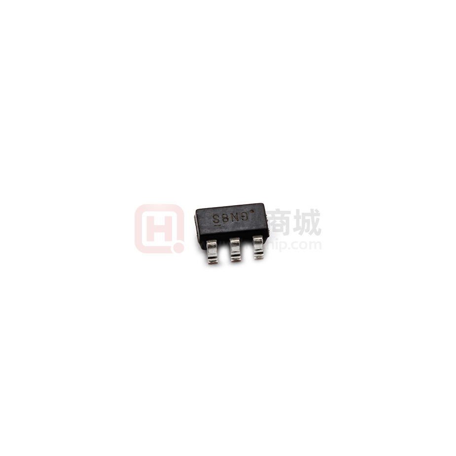
�BL8033
ORDERING INFORMATION
Mark Explanation
BST
EN
FB
6
5
4
GNYW
GN: Product Code
YW: Date code (Year & Week)
1
2
3
GND
SW
VIN
Ordering Information
Product ID
BL8033CB6TR
SOT23-6
Package
Devices per reel
3000
ABSOLUTE MAXIMUM RATING
Parameter
Value
Supply Voltage VIN
Switch Node Voltage VSW
Boost Voltage VBST
Enable Voltage VEN
All Other Pins
Operating Temperature Range
Storage Temperature Range
Lead Temperature (Soldering, 10s)
-0.3V to 17V
-0.3V to (VIN+0.5V)
VSW-0.3V to VSW+5V
-0.3V to 17V
-0.3V to 6V
-40C to 85C
-65C to 150C
300C
ELECTRICAL CHARACTERISTICS
(VIN=12V, VOUT=5V, TA=25C, unless otherwise stated)
Parameter
Conditions
Input Voltage Range
UVLO Threshold
Supply Current in Operation
Supply Current in Shutdown
Regulated Feedback Voltage
High-side Switch On Resistance
Low-side Switch On Resistance
High-side Switch Leakage Current
Upper Switch Current Limit
Oscillation Frequency
Maximum Duty Cycle
Minimum On Time
EN Input Voltage “H”
EN Input Voltage “L”
Thermal Shutdown
Min
Typ
4.2
VEN = 2.0V, VFB = 1.1V
VEN = 0V or VEN = GND
4.2V≤VIN ≤16V
VBST-SW = 5V
VIN = 5V
VEN = 0V, VSW = 0V
Minimum Duty Cycle
0.784
VFB = 0.7V
4.1
0.5
5
0.8
120
60
0
6
500
92
100
Max
Unit
16
V
V
mA
uA
V
mΩ
mΩ
uA
A
KHz
%
ns
V
V
°C
10
0.816
10
1.5
0.6
160
PIN DESCRIPTION
PIN #
NAME
DESCRIPTION
1
2
3
GND
SW
VIN
4
FB
5
EN
6
BST
Ground
Switching Pin
Power supply Pin
Adjustable version feedback input. Connect FB to the center point of the external resistor
divider.
Drive this pin to a logic-high to enable the IC. Drive to a logic-low to disable the IC and
enter micro-power shutdown mode.
Boostrap. A capacitor connected between SW and BST pins is required to form a floating
supply across the high-side switch driver.
www.belling.com.cn
2
�BL8033
ELECTRICAL PERFORMANCE
Tested under, L=4.7uH, TA=25C, unless otherwise specified
Efficiency vs. Iout
Efficiency vs. Iout
(Vout=1.2V)
(Vout=3.3V)
90%
90%
80%
80%
70%
70%
Efficiency(%)
100%
Efficiency(%)
100%
60%
50%
40%
30%
60%
50%
40%
Vin=5V
Vin=6V
Vin=12V
Vin=16V
30%
20%
20%
Vin=5V
Vin=12V
Vin=16V
10%
0%
0.0
0.5
1.0
1.5
Iout (A)
2.0
2.5
10%
0%
3.0
0.0
Efficiency vs. Iout
0.5
1.0
2.5
3.0
(Vout=1.2V)
100%
1.30
90%
1.25
80%
1.20
70%
1.15
60%
Vout (V)
Efficiency(%)
2.0
Vout vs. Iout
(Vout=5.0V)
50%
40%
30%
1.10
1.05
1.00
Vin=6V
Vin=12V
Vin=16V
20%
10%
0%
0.0
0.5
1.0
1.5
Iout (A)
2.0
2.5
Vin=5V
Vin=12V
Vin=16V
0.95
0.90
0.0
3.0
1.0
(Vout=5.0V)
3.50
3.45
3.40
3.35
Vout (V)
3.30
3.25
3.20
3.15
Vin=5V
Vin=6V
Vin=12V
Vin=16V
3.10
3.05
3.00
1.0
2.0
3.0
5.5
5.4
5.3
5.2
5.1
5.0
4.9
4.8
4.7
4.6
4.5
4.4
4.3
4.2
4.1
4.0
Vin=6V
Vin=12V
Vin=16V
0.0
Iout (A)
www.belling.com.cn
3.0
Vout vs. Iout
(Vout=3.3V)
0.0
2.0
Iout (A)
Vout vs. Iout
Vout (V)
1.5
Iout (A)
0.5
1.0
Iout (A)
3
1.5
2.0
�BL8033
Efficiency vs. Vin
Vout vs. Vin
Iout=1A
Iout=1A
98%
3.40
Vout=3.3V
97%
3.35
96%
3.30
94%
Vout (V)
Efficiency(%)
95%
93%
92%
3.25
3.20
91%
90%
3.15
89%
88%
3.10
6
8
10
12
Vin (V)
14
16
6
8
10
12
Vin(V)
14
Load Transient
Load Transient
Vin=12V, Vout=3.3V, Iout=0.01~3A
Ch2—Vout, Ch4--IL
Vin=12V, Vout=3.3V, Iout=0.5~3A
Ch2—Vout, Ch4--IL
BLOCK DIAGRAM
www.belling.com.cn
4
16
�BL8033
DETAILED DESCRIPTION
starts first, generating stable reference voltage and
currents, and then the internal regulator is enabled.
The regulator provides stable supply for the
remaining circuitries. Three events can shut down
the chip: EN low, VIN low and thermal shutdown.
In the shutdown procedure, the signaling path is
first blocked to avoid any fault triggering. The
COMP voltage and the internal supply rail are then
pulled down. The floating driver is not subject to
this shutdown command.
Internal Regulator
The BL8033 is a current mode step down DC/DC
converter that provides excellent transient
response with no extra external compensation
components. This device contains an internal, low
resistance, high voltage power MOSFET, and
operates at a high 500K operating frequency to
ensure a compact, high efficiency design with
excellent AC and DC performance.
Error Amplifier
APPLICATIONS INFORMATION
The error amplifier compares the FB pin voltage
with the internal FB reference (VFB) and outputs a
current proportional to the difference between the
two. This output current is then used to charge or
discharge the internal compensation network to
form the COMP voltage, which is used to control
the power MOSFET current. The optimized internal
compensation network minimizes the external
component counts and simplifies the control loop
design.
Setting Output Voltages
The external resistor divider is used to set the
output voltage (see Typical Application on page 1).
The feedback resistor R1 also sets the feedback
loop bandwidth with the internal compensation
capacitor. Choose R1 to be around 300kΩ for
optimal transient response. R2 is then given by:
Internal Soft-Start
The soft-start is important for many applications
because it eliminates power-up initialization
problems. The controlled voltage ramp of the
output also reduces peak inrush current during
start-up, minimizing start-up transient events to the
input power bus.
Selecting the Inductor
Over-Current-Protection and Hiccup
Use a 2.2μH-to-10μH inductor with a DC current
rating of at least 25% percent higher than the
maximum load current for most applications. For
highest efficiency, select an inductor with a DC
resistance less than 15mΩ. For most designs,
derive the inductance value from the following
equation.
The BL8033 has a cycle-by-cycle over-current
limit for when the inductor current peak value
exceeds the set current-limit threshold. First,
when the output voltage drops until FB falls
below the Under-Voltage (UV) threshold
(typically 140mV) to trigger a UV event, the
BL8033 enters hiccup mode to periodically restart
the part. This protection mode is especially useful
when the output is dead-shorted to ground. This
greatly reduces the average short-circuit current
to alleviate thermal issues and to protect the
regulator. The BL8033 exits hiccup mode once
the overcurrent condition is removed.
Where ΔIL is the inductor ripple current. Choose
an inductor current approximately 30% of the
maximum load current. The maximum inductor
peak current is:
Startup and Shutdown
Under light-load conditions (below 100mA), use
a larger inductor to improve efficiency.
If both VIN and EN are higher than their appropriate
thresholds, the chip starts. The reference block
www.belling.com.cn
5
�BL8033
ground and GND pin as short and wide as
possible.
2) Keep the connection between the input
capacitor and VIN pin as short and wide as
possible.
3) Use short and direct feedback connections.
Place the feedback resistors and compensation
components as close to the chip as possible.
4) Route SW away from sensitive analog areas
such as FB.
Selecting the Output Capacitor
The output capacitor (C2) maintains the DC
output voltage. Use ceramic, tantalum, or lowESR electrolytic capacitors. Use low ESR
capacitors to limit the output voltage ripple.
Estimate the output voltage ripple with:
Where L is the inductor value and RESR is the
equivalent series resistance (ESR) of the output
capacitor.
For ceramic capacitors, the capacitance
dominates the impedance at the switching
frequency and causes most of the output voltage
ripple. For simplification, estimate the output
voltage ripple with:
For tantalum or electrolytic capacitors, the ESR
dominates the impedance at the switching
frequency. For simplification, the output ripple
can be approximated with:
The characteristics of the output capacitor also
affect the stability of the regulation system. The
BL8033 can be optimized for a wide range of
capacitance and ESR values.
PC BOARD LAYOUT
PCB layout is very important to achieve stable
operation. For best results, use the following
guidelines and figures as reference.
1) Keep the connection between the input
www.belling.com.cn
6
�BL8033
TYPICAL APPLICATION CIRCUITS
BL8033
Figure3. 12V VIN, 5V/3A
BL8033
Figure4. 12V VIN, 3.3V/3A
BL8033
Figure5. 12V VIN, 2.5V/3A
www.belling.com.cn
7
�BL8033
BL8033
Figure6. 12V VIN, 1.8V/3A
BL8033
Figure7. 12V VIN, 1.2V/3A
PACKAGE OUTLINE
Package
SOT23-6
Devices per reel
Package specification:
www.belling.com.cn
8
3000
Unit
mm
�


 工商网监
湘ICP备2023018690号
工商网监
湘ICP备2023018690号
