BD745, BD745A, BD745B, BD745C
NPN SILICON POWER TRANSISTORS
●
Designed for Complementary Use with the
BD746 Series
●
115 W at 25°C Case Temperature
●
20 A Continuous Collector Current
●
25 A Peak Collector Current
●
Customer-Specified Selections Available
SOT-93 PACKAGE
(TOP VIEW)
B
1
C
2
E
3
Pin 2 is in electrical contact with the mounting base.
MDTRAAA
absolute maximum ratings at 25°C case temperature (unless otherwise noted)
RATING
SYMBOL
Collector-base voltage (IE = 0)
Collector-emitter voltage (IB = 0)
E
T
E
L
O
S
B
O
BD745B
V CBO
70
90
BD745C
110
BD745
45
BD745A
BD745B
UNIT
50
BD745
BD745A
VALUE
VCEO
BD745C
60
80
V
V
100
VEBO
5
V
IC
20
A
ICM
25
A
IB
7
A
Continuous device dissipation at (or below) 25°C case temperature (see Note 2)
Ptot
115
W
Continuous device dissipation at (or below) 25°C free air temperature (see Note 3)
Ptot
3.5
W
½LIC2
90
mJ
Operating free air temperature range
TA
-65 to +150
°C
Operating junction temperature range
Tj
-65 to +150
°C
Tstg
-65 to +150
°C
TL
260
°C
Emitter-base voltage
Continuous collector current
Peak collector current (see Note 1)
Continuous base current
Unclamped inductive load energy (see Note 4)
Storage temperature range
Lead temperature 3.2 mm from case for 10 seconds
NOTES: 1.
2.
3.
4.
This value applies for tp ≤ 0.3 ms, duty cycle ≤ 10%.
Derate linearly to 150°C case temperature at the rate of 0.92 W/°C.
Derate linearly to 150°C free air temperature at the rate of 28 mW/°C.
This rating is based on the capability of the transistor to operate safely in a circuit of: L = 20 mH, IB(on) = 0.4 A, RBE = 100 Ω,
VBE(off) = 0, RS = 0.1 Ω, VCC = 20 V.
������
�
�������
AUGUST 1978 - REVISED SEPTEMBER 2002
Specifications are subject to change without notice.
1
�BD745, BD745A, BD745B, BD745C
NPN SILICON POWER TRANSISTORS
electrical characteristics at 25°C case temperature (unless otherwise noted)
PARAMETER
V(BR)CEO
ICBO
ICEO
IEBO
hFE
VCE(sat)
VBE
hfe
|hfe |
Collector-emitter
TEST CONDITIONS
MIN
45
BD745A
60
BD745B
80
BD745C
100
TYP
MAX
IC = 30 mA
IB = 0
VCE = 50 V
VBE = 0
BD745
0.1
VCE = 70 V
VBE = 0
BD745A
0.1
VCE = 90 V
VBE = 0
BD745B
0.1
Collector cut-off
VCE = 110 V
VBE = 0
BD745C
0.1
current
VCE = 50 V
VBE = 0
TC = 125°C
BD745
5
VCE = 70 V
VBE = 0
TC = 125°C
BD745A
5
VCE = 90 V
VBE = 0
TC = 125°C
BD745B
5
VCE = 110 V
VBE = 0
TC = 125°C
BD745C
Collector cut-off
VCE = 30 V
IB = 0
BD745/745A
0.1
current
VCE = 60 V
IB = 0
BD745B/745C
0.1
VEB =
5V
IC = 0
VCE =
4V
IC = 1 A
breakdown voltage
Emitter cut-off
current
Forward current
transfer ratio
Collector-emitter
saturation voltage
Base-emitter
voltage
Small signal forward
current transfer ratio
Small signal forward
current transfer ratio
(see Note 5)
BD745
4V
IC = 5 A
VCE =
4V
IC = 20 A
V
mA
5
0.5
mA
mA
40
E
T
E
L
O
S
B
O
VCE =
UNIT
(see Notes 5 and 6)
20
150
5
IB =
0.5 A
IC = 5 A
IB =
5A
IC = 20 A
VCE =
4V
IC = 5 A
VCE =
4V
IC = 20 A
VCE = 10 V
IC = 1 A
f = 1 kHz
25
VCE = 10 V
IC = 1 A
f = 1 MHz
5
1
(see Notes 5 and 6)
3
1
(see Notes 5 and 6)
3
V
V
NOTES: 5. These parameters must be measured using pulse techniques, tp = 300 µs, duty cycle ≤ 2%.
6. These parameters must be measured using voltage-sensing contacts, separate from the current carrying contacts.
thermal characteristics
MAX
UNIT
RθJC
Junction to case thermal resistance
PARAMETER
MIN
TYP
1.1
°C/W
RθJA
Junction to free air thermal resistance
35.7
°C/W
MAX
UNIT
resistive-load-switching characteristics at 25°C case temperature
PARAMETER
†
TEST CONDITIONS
†
MIN
td
Delay time
20
ns
tr
Rise time
IC = 5 A
IB(on) = 0.5 A
IB(off) = -0.5 A
350
ns
ts
Storage time
VBE(off) = -4.2 V
RL = 6 Ω
tp = 20 µs, dc ≤ 2%
500
ns
tf
Fall time
400
ns
Voltage and current values shown are nominal; exact values vary slightly with transistor parameters.
������
2
TYP
�
�������
AUGUST 1978 - REVISED SEPTEMBER 2002
Specifications are subject to change without notice.
�BD745, BD745A, BD745B, BD745C
NPN SILICON POWER TRANSISTORS
TYPICAL CHARACTERISTICS
TYPICAL DC CURRENT GAIN
vs
COLLECTOR CURRENT
COLLECTOR-EMITTER SATURATION VOLTAGE
vs
COLLECTOR CURRENT
hFE - DC Current Gain
TC = 125°C
TC = 25°C
TC = -55°C
0·1
1·0
IC
= 10
IB
tp = 300µs, duty cycle < 2%
1·0
0·1
E
T
E
L
O
S
B
O
VCE = 4 V
tp = 300 µs, duty cycle < 2%
10
TCS635AF
10
VCE(sat) - Collector-Emitter Saturation Voltage - V
TCS635AE
100
10
100
0·01
0·1
1·0
IC - Collector Current - A
TC = -55°C
TC = 25°C
TC = 125°C
10
100
IC - Collector Current - A
Figure 1.
Figure 2.
MAXIMUM SAFE OPERATING REGIONS
MAXIMUM FORWARD-BIAS
SAFE OPERATING AREA
IC - Collector Current - A
100
SAS635AC
tp = 1 ms,
d = 0.1 = 10%
tp = 10 ms,
d = 0.1 = 10%
tp = 50 ms,
d = 0.1 = 10%
DC Operation
10
1·0
0·1
BD745
BD745A
BD745B
BD745C
0·01
1·0
10
100
1000
VCE - Collector-Emitter Voltage - V
Figure 3.
������
�
�������
AUGUST 1978 - REVISED SEPTEMBER 2002
Specifications are subject to change without notice.
3
�BD745, BD745A, BD745B, BD745C
NPN SILICON POWER TRANSISTORS
THERMAL INFORMATION
MAXIMUM POWER DISSIPATION
vs
CASE TEMPERATURE
TIS635AB
Ptot - Maximum Power Dissipation - W
120
100
80
60
40
E
T
E
L
O
S
B
O
20
0
0
25
50
75
100
125
150
TC - Case Temperature - °C
Figure 4.
������
4
�
�������
AUGUST 1978 - REVISED SEPTEMBER 2002
Specifications are subject to change without notice.
�
很抱歉,暂时无法提供与“BD745A-S”相匹配的价格&库存,您可以联系我们找货
免费人工找货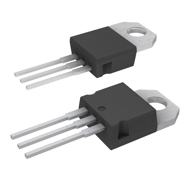


 工商网监
湘ICP备2023018690号
工商网监
湘ICP备2023018690号
