BUT11 NPN SILICON POWER TRANSISTOR
● ● ●
Rugged Triple-Diffused Planar Construction 100 W at 25°C Case Temperature 5 A Continuous Collector Current
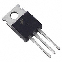
B C E
1 2 3 TO-220 PACKAGE (TOP VIEW)
Pin 2 is in electrical contact with the mounting base.
MDTRACA
absolute maximum ratings at 25°C case temperature (unless otherwise noted)
RATING Collector-base voltage (IE = 0) Collector-emitter voltage (VBE = 0) Collector-emitter voltage (IB = 0) Emitter-base voltage Continuous collector current Peak collector current (see Note 1) Continuous device dissipation at (or below) 25°C case temperature Operating junction temperature range Storage temperature range NOTE 1: This value applies for tp ≤ 10 ms, duty cycle ≤ 2%. SYMBOL VCBO VCES V CEO VEBO IC ICM Ptot Tj Tstg VALUE 850 850 400 10 5 10 100 -65 to +150 -65 to +150 UNIT V V V V A A W °C °C
MAY 1989 - REVISED SEPTEMBER 2002 Specifications are subject to change without notice.
NOITAMROFNI
TCUDORP
1
�BUT11 NPN SILICON POWER TRANSISTOR
electrical characteristics at 25°C case temperature (unless otherwise noted)
PARAMETER VCEO(sus) ICES IEBO hFE VCE(sat) VBE(sat) ft Cob Collector-emitter sustaining voltage Collector-emitter cut-off current Emitter cut-off current Forward current transfer ratio Collector-emitter saturation voltage Base-emitter saturation voltage Current gain bandwidth product Output capacitance IC = 0.1 A TEST CONDITIONS L = 25 mH VBE = 0 VBE = 0 IC = 0 IC = 0.5 A IC = IC = 3A 3A (see Notes 3 and 4) (see Notes 3 and 4) (see Notes 3 and 4) f= 1 MHz 12 110 20 TC = 125°C (see Note 2) MIN 400 50 500 1 60 1.5 1.3 V V MHz pF TYP MAX UNIT V µA mA
VCE = 850 V VCE = 850 V VEB = VCE = IB = IB = VCE = VCB = 10 V 5V 0.6 A 0.6 A 10 V 20 V
IC = 0.5 A IE = 0
f = 0.1 MHz
NOTES: 2. Inductive loop switching measurement. 3. These parameters must be measured using pulse techniques, tp = 300 µs, duty cycle ≤ 2%. 4. These parameters must be measured using voltage-sensing contacts, separate from the current carrying contacts.
thermal characteristics
PARAMETER RθJC Junction to case thermal resistance MIN TYP MAX 1.25 UNIT °C/W
inductive-load-switching characteristics at 25°C case temperature (unless otherwise noted)
PARAMETER tsv tfi tsv tfi
†
TEST CONDITIONS IC = 3 A VCC = 50 V IC = 3 A VCC = 50 V IB(on) = 0.6A
†
MIN VBE(off) = -5 V VBE(off) = -5 V
TYP
MAX 1.4 150 1.5 300
UNIT µs ns µs ns
Voltage storage time Current fall time Voltage storage time Current fall time
(see Figures 1 and 2) IB(on) = 0.6A TC = 100°C
Voltage and current values shown are nominal; exact values vary slightly with transistor parameters.
2
MAY 1989 - REVISED SEPTEMBER 2002 Specifications are subject to change without notice.
NOITAMROFNI
TCUDORP
�BUT11 NPN SILICON POWER TRANSISTOR
PARAMETER MEASUREMENT INFORMATION
33 Ω
+5V
D45H11 BY205-400 BY205-400
33 Ω 1 pF
RB
(on) 180 µ H vcc
V Gen 68 Ω
1 kΩ 0.02 µ F +5V 1 kΩ
2N2222 TUT BY205-400 Vclamp = 400 V
270 Ω
BY205-400
1 kΩ 2N2904
5X BY205-400
Adjust pw to obtain IC 47 Ω For IC < 6 A For IC ≥ 6 A VCC = 50 V VCC = 100 V 100 Ω
D44H11 V BE(off)
Figure 1. Inductive-Load Switching Test Circuit
I B(on) A - B = tsv B - C = trv D - E = tfi E - F = tti B - E = txo IB
A (90%) Base Current
C
90%
V CE
B
10%
Collector Voltage
D (90%)
E (10%) I C(on) Collector Current F (2%)
NOTES: A. Waveforms are monitored on an oscilloscope with the following characteristics: t r < 15 ns, Rin > 10 Ω, C in < 11.5 pF. B. Resistors must be noninductive types.
Figure 2. Inductive-Load Switching Waveforms
MAY 1989 - REVISED SEPTEMBER 2002 Specifications are subject to change without notice.
NOITAMROFNI
TCUDORP
3
�BUT11 NPN SILICON POWER TRANSISTOR
MAXIMUM SAFE OPERATING REGIONS
MAXIMUM FORWARD-BIAS SAFE OPERATING AREA
100
SAP791AB
IC - Collector Current - A
10
1·0
0.1
tp =
10 µ s
tp = 100 µ s tp = 1 ms tp = 10 ms DC Operation 10 100 1000
0·01 1·0
VCE - Collector-Emitter Voltage - V
Figure 3.
4
MAY 1989 - REVISED SEPTEMBER 2002 Specifications are subject to change without notice.
NOITAMROFNI
TCUDORP
�BUT11 NPN SILICON POWER TRANSISTOR
MECHANICAL DATA TO-220 3-pin plastic flange-mount package
This single-in-line package consists of a circuit mounted on a lead frame and encapsulated within a plastic compound. The compound will withstand soldering temperature with no deformation, and circuit performance characteristics will remain stable when operated in high humidity conditions. Leads require no additional cleaning or processing when used in soldered assembly.
TO220 4,70 4,20
ø
3,96 3,71
10,4 10,0
2,95 2,54 6,6 6,0 15,90 14,55
1,32 1,23
see Note B
see Note C
6,1 3,5
0,97 0,61 1 2 3
1,70 1,07
14,1 12,7
2,74 2,34 5,28 4,88 2,90 2,40
0,64 0,41
VERSION 1
VERSION 2
ALL LINEAR DIMENSIONS IN MILLIMETERS NOTES: A. The centre pin is in electrical contact with the mounting tab. B. Mounting tab corner profile according to package version. C. Typical fixing hole centre stand off height according to package version. Version 1, 18.0 mm. Version 2, 17.6 mm. MDXXBE
MAY 1989 - REVISED SEPTEMBER 2002 Specifications are subject to change without notice.
NOITAMROFNI
TCUDORP
5
�
很抱歉,暂时无法提供与“BUT11”相匹配的价格&库存,您可以联系我们找货
免费人工找货- 国内价格
- 1+2.58668
- 10+2.3877
- 30+2.34791
- 100+2.22852


 工商网监
湘ICP备2023018690号
工商网监
湘ICP备2023018690号

