TISP4125H3BJ/TISP4219H3BJ,
TISP4125M3BJ/TISP4219M3BJ
LCAS RING AND TIP PROTECTION PAIRS
BIDIRECTIONAL THYRISTOR OVERVOLTAGE PROTECTORS
TISP4xxxH3/M3BJ Series for LCAS Protection
Customized Voltage for LCAS Protection
Battery-Backed Ringing�������������� 87 V rms
Ground-Backed Ringing������������101 V rms
Device
VDRM
V
V(BO)
V
LCAS
TERMINAL
‘4125
100
125
TIP
‘4219
180
219
RING
Low Differential Capacitance��� 39 pF max.
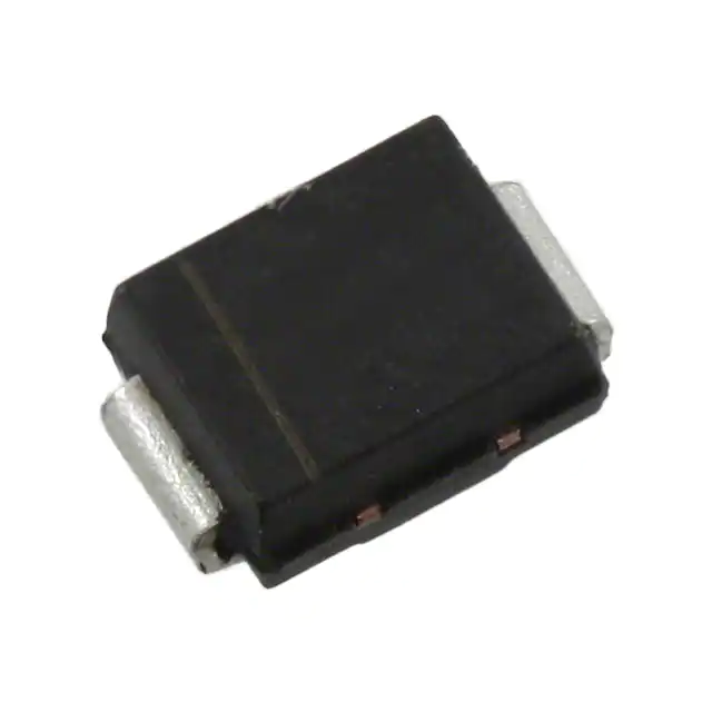
SMBJ Package (Top View)
Additional Information
Click these links for more information:
2 T(A)
R(B) 1
MDXXBGE
CONTACT
Description
These protector pairs have been formulated
to limit the peak voltages on the line
terminals of the ‘7581/2/3 LCAS (Line
Card Access Switches) type devices. An
LCAS may also be referred to as a Solid
State Relay, SSR, i.e. a replacement of the
conventional electro-mechanical relay.
Device Symbol
T
��������������������UL Recognized Components
Rated for International Surge Wave
Shapes
R
SD4XAA
Terminals T and R correspond to the
alternative line designators of A and B
Wave Shape
PRODUCT TECHNICAL INVENTORY SAMPLES
SELECTOR LIBRARY
ITSP
A
Standard
H3 Series
M3 Series
2/10 µs
GR-1089-CORE
500
300
8/20 µs
IEC 61000-4-5
300
220
10/160 µs
FCC Part 68
250
120
10/700 µs
ITU-T K.20/21/45
200
100
10/560 µs
FCC Part 68
160
75
10/1000 µs
GR-1089-CORE
100
50
Overvoltages are normally caused by a.c.
power system or lightning flash disturbances
which are induced or conducted on to the
telephone line. These overvoltages are
initially clipped by protector breakdown
clamping until the voltage rises to the
breakover level, which causes the device
to crowbar into a low-voltage on state. This
low-voltage on state causes the current
resulting from the overvoltage to be safely
diverted through the device. For negative
surges, the high crowbar holding current
helps prevent d.c. latchup with the SLIC
current, as the surge current subsides.
Each protector consists of a symmetrical
voltage-triggered bidirectional thyristor.
They are guaranteed to voltage limit and
withstand the listed international lightning
surges in both polarities.
How to Order
Device
Package
Carrier
TISP4125H3BJ
TISP4219H3BJ
TISP4125M3BJ
Order As
TISP4125H3BJR-S
BJ (J-Bend DO-214AA/SMB) Embossed Tape Reeled
TISP4219M3BJ
TISP4219H3BJR-S
TISP4125M3BJR-S
TISP4219M3BJR-S
WARNING Cancer and Reproductive Harm
www.P65Warnings.ca.gov
JUNE 2001 – REVISED OCTOBER 2022
*RoHS Directive 2015/863, Mar 31, 2015 and Annex.
Specifications are subject to change without notice.
Users should verify actual device performance in their specific applications.
The products described herein and this document are subject to specific legal disclaimers as set forth on the last page of this document, and at www.bourns.com/docs/legal/disclaimer.pdf.
�
TISP4xxxH3/M3BJ Series for LCAS Protection
TISP4125H3BJ & TISP4219H3BJ
Absolute Maximum Ratings, TA = 25 °C (Unless Otherwise Noted)
Rating
‘4125
‘4219
Repetitive peak off-state voltage, (see Note 1)
Symbol
Non-repetitive peak on-state pulse current (see Notes 2 and 3)
2/10 µs (GR-1089-CORE, 2/10 µs voltage wave shape)
8/20 µs (IEC 61000-4-5, 1.2/50 µs voltage, 8/20 current combination wave generator)
10/160 µs (FCC Part 68, 10/160 µs voltage wave shape)
5/200 µs (VDE 0433, 10/700 µs voltage wave shape)
0.2/310 µs (I3124, 0.5/700 µs voltage wave shape)
5/310 µs (ITU-T K.20/21, 10/700 µs voltage wave shape)
5/310 µs (FTZ R12, 10/700 µs voltage wave shape)
10/560 µs (FCC Part 68, 10/560 µs voltage wave shape)
10/1000 µs (GR-1089-CORE, 10/1000 µs voltage wave shape)
Non-repetitive peak on-state current (see Notes 2, 3 and 4)
20 ms (50 Hz) full sine wave
16.7 ms (60 Hz) full sine wave
1000 s 50 Hz/60 Hz a.c.
Initial rate of rise of on-state current, Exponential current ramp, Maximum ramp value < 200 A
Junction temperature
Storage temperature range
NOTES: 1.
2.
3.
4.
Value
±100
±180
VDRM
500
300
250
220
200
200
200
160
100
ITSP
55
60
2.1
400
-40 to +150
-65 to +150
ITSM
di T/dt
TJ
Tstg
Unit
V
A
A
A/µs
°C
°C
See Applications Information for voltage values at lower temperatures.
Initially, the TISP4xxxH3BJ must be in thermal equilibrium with TJ = 25 °C..
The surge may be repeated after the TISP4xxxH3BJ returns to its initial conditions.
EIA/JESD51-2 environment and EIA/JESD51-3 PCB with standard footprint dimensions connected with 5 A rated printed wiring
track widths. See Figure 10 for the current ratings at other durations. Derate current values at -0.61 %/ °C for ambient
temperatures above 25 °C.
Recommended Operating Conditions
Component
RS
VRING
Series current limiting
resistor
AC ringing voltage
Condition
Min
Typ
Max
Unit
GR-1089-CORE first-level surge survival
0
Ω
GR-1089-CORE first-level and second-level surge survival
0
Ω
K.20, K.21 and K.45 coordination pass with a 400 V primary
protector
6
Ω
Figure 12, VBAT = -48 V ±2.5 V,
R1= R2 = 300 Ω,, 0 °C < TA < +85 °C
JUNE 2001 – REVISED OCTOBER 2022
Battery-backed
87
V rms
Ground-backed
101
V rms
Specifications are subject to change without notice.
Users should verify actual device performance in their specific applications.
The products described herein and this document are subject to specific legal disclaimers as set forth on the last page of this document, and at www.bourns.com/docs/legal/disclaimer.pdf.
�
TISP4xxxH3/M3BJ Series for LCAS Protection
Electrical Characteristics, TISP4xxxH3, TA = 25 °C (Unless Otherwise Noted)
Parameter
IDRM
Test Conditions
Repetitive peak offstate current
V(BO) Breakover voltage
Impulse breakover
V(BO)
voltage
I(BO)
VT
IH
Breakover current
On-state voltage
Holding current
ID
Critical rate of rise of
off-state voltage
Off-state current
Coff
Off-state capacitance
dv/dt
VD = VDRM
dv/dt = ±250 V/ms, R SOURCE = 300 Ω
dv/dt ≤ ±1000 V/µs, Linear voltage ramp,
Maximum ramp value = ±500 V
di/dt = ±20 A/µs, Linear current ramp,
Maximum ramp value = ±10 A
dv/dt = ±250 V/ms, R SOURCE = 300 Ω
I T = ±5 A, t W = 100 µs
I T = ±5A , di/dt = +/-30 mA/ms
TA = 25 °C
TA = 85 °C
‘4125
‘4219
Typ
‘4125
‘4219
±0.15
±0.15
Max
±5
±10
±125
±219
TA = 85 °C
Unit
µA
V
±134
±229
V
±0.6
±3
± 0.6
A
V
A
±5
Linear voltage ramp, Maximum ramp value < 0.85V DRM
V D = ± 50 V
f = 1 MHz, Vd = 1 V rms, VD = 0,
f = 1 MHz, Vd = 1 V rms, VD = -1 V
f = 1 MHz, Vd = 1 V rms, VD = -2 V
f = 1 MHz, Vd = 1 V rms, VD = -50 V
f = 1 MHz, Vd = 1 V rms, VD = -100 V
(see Note 5)
Min
kV/µs
80
71
65
30
23
±10
90
79
74
35
28
µA
Typ
Max
Unit
pF
NOTE 5: To avoid possible voltage clipping, the ‘4125 is tested with VD = -98 V.
Thermal Characteristics
Parameter
R θJA Junction to free air thermal resistance
NOTE
Test Conditions
Min
EIA/JESD51-3 PCB, IT = ITSM(1000) ,
TA = 25 °C, (see Note 6)
265 mm x 210 mm populated line card,
4-layer PCB, IT = ITSM(1000) , TA = 25 °C
113
°C/W
50
6: EIA/JESD51-2 environment and the PCB has standard foot print dimensions connect ed with 5 A rated printed wiring track widths.
JUNE 2001 – REVISED OCTOBER 2022
Specifications are subject to change without notice.
Users should verify actual device performance in their specific applications.
The products described herein and this document are subject to specific legal disclaimers as set forth on the last page of this document, and at www.bourns.com/docs/legal/disclaimer.pdf.
�
TISP4xxxH3/M3BJ Series for LCAS Protection
TISP4125M3BJ & TISP4219M3BJ
Absolute Maximum Ratings, TA = 25 °C (Unless Otherwise Noted)
Rating
‘4125
‘4219
Repetitive peak off-state voltage, (see Note 7)
Symbol
Non-repetitive peak on-state pulse current (see Notes 8 and 9)
2/10 µs (GR-1089-CORE, 2/10 µs voltage wave shape)
8/20 µs (IEC 61000-4-5, 1.2/50 µs voltage, 8/20 current combination wave generator)
10/160 µs (FCC Part 68, 10/160 µs voltage wave shape)
5/200 µs (VDE 0433, 10/700 µs voltage wave shape)
0.2/310 µs (I3124, 0.5/700 µs voltage wave shape)
5/310 µs (ITU-T K.20/21, 10/700 µs voltage wave shape)
5/310 µs (FTZ R12, 10/700 µs voltage wave shape)
10/560 µs (FCC Part 68, 10/560 µs voltage wave shape)
10/1000 µs (GR-1089-CORE, 10/1000 µs voltage wave shape)
Non-repetitive peak on-state current (see Notes 8, 9 and 10)
20 ms (50 Hz) full sine wave
16.7 ms (60 Hz) full sine wave
1000 s 50 Hz/60 Hz a.c.
Initial rate of rise of on-state current, Exponential current ramp, Maximum ramp value < 200 A
Junction temperature
Storage temperature range
VDRM
Value
±100
±180
300
220
120
110
100
100
100
75
50
ITSP
di T/dt
TJ
Tstg
V
A
30
32
2.1
300
-40 to +150
-65 to +150
ITSM
Unit
A
A/µs
°C
°C
NOTES: 7. See Applications Information for voltage values at lower temperatures.
8. Initially, the TISP4xxxM3BJ must be in thermal equilibrium with TJ = 25 °C.
9. The surge may be repeated after the TISP4xxxM3BJ returns to its initial conditions.
10.EIA/JESD51-2 environment and EIA/JESD51-3 PCB with standard footprint dimensions connected with 5 A rated printed wiring
track widths. See Figure 11 for the current ratings at other durations. Derate current values at -0.61 %/ °C for ambient
temperatures above 25 °C.
Recommended Operating Conditions
Component
RS
VRING
Series current limiting
resistor
AC ringing voltage
Condition
Min
Typ
Max
Unit
GR-1089-CORE first-level surge survival
10
Ω
GR-1089-CORE first-level and second-level surge survival
12
Ω
6
Ω
K.20, K.21 and K.45 coordination pass with a 400 V primary
protector
Figure 12, VBAT = -48 V ±2.5 V,
R1= R2 = 300 Ω, 0 °C < TA < +85 °C
JUNE 2001 – REVISED OCTOBER 2022
Battery-backed
87
V rms
Ground-backed
101
V rms
Specifications are subject to change without notice.
Users should verify actual device performance in their specific applications.
The products described herein and this document are subject to specific legal disclaimers as set forth on the last page of this document, and at www.bourns.com/docs/legal/disclaimer.pdf.
�
TISP4xxxH3/M3BJ Series for LCAS Protection
Electrical Characteristics, TISP4xxxM3, TA = 25 °C (Unless Otherwise Noted)
Parameter
IDRM
V(BO) Breakover voltage
Impulse breakover
V(BO)
voltage
I(BO)
VT
IH
ID
Breakover current
On-state voltage
Holding current
Critical rate of rise of
off-state voltage
Off-state current
Coff
Off-state capacitance
dv/dt
Test Conditions
Repetitive peak offstate current
VD = VDRM
dv/dt = ±250 V/ms, R SOURCE = 300 Ω
dv/dt ≤ ±1000 V/s, Linear voltage ramp,
Maximum ramp value = ±500 V
di/dt = ±20 A/µs, Linear current ramp,
Maximum ramp value = ±10 A
dv/dt = ±250 V/ms, R SOURCE = 300 Ω
IT = ±5 A, t W = 100 µs
IT = ±5A, di/dt = +/-30 mA/ms
TA = 25 °C
TA = 85 °C
‘4125
‘4219
VD = 0,
VD = -1 V
VD = -2 V
VD = -50 V
VD = -100 V
Typ
‘4125
‘4219
Max
±5
±10
±125
±219
±132
±226
±0.15
±0.6
±3
±0.15
±0.6
±5
Linear voltage ramp, Maximum ramp value < 0.85V DRM
V D = ±50 V
f = 1 MHz, Vd = 1 V rms,
f = 1 MHz, Vd = 1 V rms,
f = 1 MHz, Vd = 1 V rms,
f = 1 MHz, Vd = 1 V rms,
f = 1 MHz, Vd = 1 V rms,
(see Note 11)
Min
TA = 85 °C
Unit
µA
V
V
A
V
A
kV/µs
62
56
52
26
21
±10
74
67
62
31
25
µA
Typ
Max
Unit
pF
NOTE 11: To avoid possible voltage clipping, the ‘4125 is tested with VD = -98 V.
Thermal Characteristics
Parameter
R θJA Junction to free air thermal resistance
Test Conditions
Min
EIA/JESD51-3 PCB, IT = ITSM(1000) ,
TA = 25 °C, (see Note 12)
265 mm x 210 mm populated line card,
4-layer PCB, IT = ITSM(1000) , TA = 25 °C
115
°C/W
52
NOTE 12: EIA/JESD51-2 environment and the PCB has standard foot print dimensions connected with 5 A rated printed wiring track widt hs.
JUNE 2001 – REVISED OCTOBER 2022
Specifications are subject to change without notice.
Users should verify actual device performance in their specific applications.
The products described herein and this document are subject to specific legal disclaimers as set forth on the last page of this document, and at www.bourns.com/docs/legal/disclaimer.pdf.
�
TISP4xxxH3/M3BJ Series for LCAS Protection
Parameter Measurement Information
+i
ITSP
Quadrant I
Switching
Characteristic
ITSM
IT
V(BO)
VT
I(BO)
IH
VDRM
-v
IDRM
ID
VD
ID
IDRM
VD
VDRM
+v
IH
I(BO)
VT
V(BO)
IT
ITSM
I
Quadrant III
ITSP
Switching
Characteristic
-i
PMXXAAB
Figure 1. Voltage-Current Characteristic for T and R Terminals
All Measurements are Referenced to the R Terminal
JUNE 2001 – REVISED OCTOBER 2022
Specifications are subject to change without notice.
Users should verify actual device performance in their specific applications.
The products described herein and this document are subject to specific legal disclaimers as set forth on the last page of this document, and at www.bourns.com/docs/legal/disclaimer.pdf.
�
TISP4xxxH3/M3BJ Series for LCAS Protection
TISP4xxxH3BJ Typical Characteristics
OFF-STATE CURRENT
vs
JUNCTION TEMPERATURE
100
TCHAG
VD = ±50 V
TC4HAF
Normalized Breakover Voltage
|ID| - Off-State Current - µA
10
1.10
NORMALIZED BREAKOVER VOLTAGE
vs
JUNCTION TEMPERATURE
1.05
1
0·1
1.00
0·01
0·001
-25
0
25
50
75
100 125
TJ - Junction Temperature - °C
150
0.95
-25
Figure 2.
ON-STATE CURRENT
vs
ON-STATE VOLTAGE
IT - On-State Current - A
100
70
50
40
30
TC4HACC
2.0
TA = 25 °C
t W = 100 µs
NORMALIZED HOLDING CURRENT
vs
JUNCTION TEMPERATURE
TC4HAD
1.5
20
15
10
7
5
4
3
1.0
0.9
0.8
0.7
0.6
0.5
2
1.5
1
0.7
150
Figure 3.
Normalized Holding Current
200
150
0
25
50
75
100 125
TJ - Junction Temperature - °C
1
1.5
2
3
4 5
VT - On-State Voltage - V
Figure 4.
JUNE 2001 – REVISED OCTOBER 2022
7
10
0.4
-25
0
25
50
75
100
TJ - Junction Temperature - °C
125
150
Figure 5.
Specifications are subject to change without notice.
Users should verify actual device performance in their specific applications.
The products described herein and this document are subject to specific legal disclaimers as set forth on the last page of this document, and at www.bourns.com/docs/legal/disclaimer.pdf.
�
TISP4xxxH3/M3BJ Series for LCAS Protection
TISP4xxxM3BJ Typical Characteristics
100
OFF-STATE CURRENT
vs
JUNCTION TEMPERATURE
TCMAG
VD = ±50 V
Normalized Breakover Voltage
10
|ID| - Off-State Current - µA
1.10
NORMALIZED BREAKOVER VOLTAGE
vs
JUNCTION TEMPERATURE
TC4MAF
1.05
1
0·1
1.00
0·01
0·001
-25
0
25
50
75
100
TJ - Junction Temperature - °C
125
0.95
150
-25
Figure 6.
ON-STATE CURRENT
vs
ON-STATE VOLTAGE
IT - On-State Current - A
70
50
40
30
TC4MACB
NORMALIZED HOLDING CURRENT
vs
JUNCTION TEMPERATURE TC4MAD
2.0
TA = 25 °C
tW = 100 µs
1.5
20
15
10
7
5
4
3
2
1.5
1
0.7
150
Figure 7.
Normalized Holding Current
100
0
25
50
75
100 125
TJ - Junct ion Temperature - °C
1.0
0.9
0.8
0.7
0.6
0.5
1
1.5
2
3
4 5
VT - On-State Voltage - V
Figure 8.
JUNE 2001 – REVISED OCTOBER 2022
7
10
0.4
-25
0
25
50
75
100 125
TJ - Junction Temperature - °C
150
Figure 9.
Specifications are subject to change without notice.
Users should verify actual device performance in their specific applications.
The products described herein and this document are subject to specific legal disclaimers as set forth on the last page of this document, and at www.bourns.com/docs/legal/disclaimer.pdf.
�
TISP4xxxH3/M3BJ Series for LCAS Protection
Rating Information
TISP4xxxH3BJ
TISP4xxxM3BJ
NON-REPETITIVE PEAK ON-STATE CURRENT
vs
CURRENT DURATION
TI4HAC
30
ITSM(t) - Non-Repetitive Peak On-State Current - A
ITSM(t) - Non-Repetitive Peak On-State Current - A
NON-REPETITIVE PEAK ON-STATE CURRENT
vs
CURRENT DURATION
VGEN = 600 Vrms, 50/60 Hz
RGEN = 1.4*VGEN/ITSM(t)
EIA/JESD51-2 ENVIRONMENT
EIA/JESD51-3 PCB
TA = 25 °C
20
15
10
9
8
7
6
5
4
3
2
1.5
0·1
1
10
100
t - Current Duration - s
Figure 10.
JUNE 2001 – REVISED OCTOBER 2022
1000
TI4MAC
30
VGEN = 600 Vrms, 50/60 Hz
RGEN = 1.4*VGEN/ITSM(t)
EIA/JESD51-2 ENVIRONMENT
EIA/JESD51-3 PCB
TA = 25 °C
20
15
10
9
8
7
6
5
4
3
2
1.5
0·1
1
10
100
1000
t - Current Duration - s
Figure 11.
Specifications are subject to change without notice.
Users should verify actual device performance in their specific applications.
The products described herein and this document are subject to specific legal disclaimers as set forth on the last page of this document, and at www.bourns.com/docs/legal/disclaimer.pdf.
�
TISP4xxxH3/M3BJ Series for LCAS Protection
APPLICATIONS INFORMATION
Introduction
These protector pairs have been designed to limit the peak voltages on the line terminals of ‘7581/7582/7583 LCAS (Line Card Access Switch)
parts. An LCAS may also be referred to as a Solid-State Relay, SSR, i.e. a replacement of the conventional electro-mechanical relay.
The ‘7581 LCAS has two solid-state switches which connect the telephone line to the line card SLIC (Subscriber Line Interface Circuit), Figure 12,
SW1 and SW2. A further two solid-state switches connect the telephone ringing generator to the line, Figure 12, SW3 and SW4. Applied 5-volt
logic signals control the condition of the switches to perform the functions of line disconnect, connection to the SLIC and application of ringing. If
excessive long-term overdissipation occurs, a thermal sensor activates thermal shutdown and opens the switches. The SLIC side of switches SW1
and SW2 is limited in voltage by internal protectors Th3 and Th4. The line-side of the LCAS is voltage limited by the two TISP® parts.
Th1
RING
RELAY
SLIC
RELAY
SW3
SW1
LCAS
Th2
RING
TISP4219M3
OR
TISP4219H3
SW4
R2
SW2
SLIC
Th3
Th4
CONTROL
LOGI C
TIP
TISP4125M3
OR
TISP4125H3
Vbat
AI4XAQ
R1
VRING
VBAT
SW5a
SW5b
RING
GENERATOR
Figure 12. Basic LCAS Arrangement
Additional functions are provided by the ‘7582 (line test access) and the ‘7583 (test-in and test-out access). Up to three conventional electromechanical relays may be replaced by the LCAS. The resulting size reduction can double the line density of a line card.
This document covers the types of overvoltage protection required by the ’7581 LCAS and how the TISP® part voltages are selected to provide
these requirements. The LCAS ’7582 and ’7583 are also covered as the additional switches used in these parts are similar to the ’7581.
JUNE 2001 – REVISED OCTOBER 2022
Specifications are subject to change without notice.
Users should verify actual device performance in their specific applications.
The products described herein and this document are subject to specific legal disclaimers as set forth on the last page of this document, and at www.bourns.com/docs/legal/disclaimer.pdf.
�
TISP4xxxH3/M3BJ Series for LCAS Protection
LCAS Switch Ratings
When a switch is in the off state, the maximum withstand voltage may be set by the switch itself or by the control line to the switch. At 25 °C,
the switch terminal to ground voltage rating for all the switches is ±320 V. Switches SW1 to SW3 are bidirectional MOS types and can withstand
±320 V between terminals. Switch SW4 is a bidirectional thyristor which is rated at ±465 V between terminals.
Overcurrents as well as overvoltages occur on telephone lines. In the on state, the thyristor switch, SW4, is capable of withstanding high levels
of current overload. For currents above about 200 mA, the MOS switches, SW1 to SW3, will go into a current limited condition. This will cause
the voltage to rise across the switch and large amounts of power to be developed. In the longer term, this power loss increases the overall chip
temperature. When the temperature exceeds about 125 °C, thermal shutdown occurs and the switches are set to the off state. Without power
loss, the LCAS will cool. Eventually, the thermal trip will reset, setting the switches back in the high power loss condition again. The cycle of
temperature increase, thermal shutdown, temperature decrease and switch re-activation will continue until the overcurrent ceases.
TISP4125M3
OR
TISP4125H3
R1
OVERCURRENT
PROTECTION
RING
SLIC
RELAY
SW3
SW1
Th1
Th3
Th4
Th2
R2
SLIC
TISP4219M3
OR
TISP4219H3
SW4
CONTROL
LOGIC
TIP
RING
RELAY
SW2
Vbat
AI4XAR
GROUND-BACKED RINGING
SW5 AS SHOWN
+√2xV RING
TIP
WIRE
R2
√2xV RING
VBAT
SW5b
0
VBAT
RING
WIRE
-√2xV RING
R1
SW5a
RING
GENERATOR
BATTERY-BACKED RINGING
SW5 OPERATED
VBAT + √2xV RING
TIP
WIRE
0
VBAT
RING
WIRE
VBAT - √2xV RING
Figure 13. LCAS Shown with Switch Breakdown Limits
Equivalent Circuit
Figure 13 shows the LCAS switch voltage ratings as breakdown diodes, which must not be allowed to conduct. Each switch has three diodes;
one between poles and the other two from each pole to ground. At 25 °C, switches SW1 through to SW3 have breakdown diode voltages of
±320 V. Switch SW4 has breakdown diode voltage values of ±465 V for the one between poles and ±320 V for the two diodes connected to
ground. Note that only protection to ground is required, as in the limit, the inter-switch voltage limitation of ±640 V is the same as the switch to
ground limitation of +320 V and -320 V in both polarities.
JUNE 2001 – REVISED OCTOBER 2022
Specifications are subject to change without notice.
Users should verify actual device performance in their specific applications.
The products described herein and this document are subject to specific legal disclaimers as set forth on the last page of this document, and at www.bourns.com/docs/legal/disclaimer.pdf.
�
TISP4xxxH3/M3BJ Series for LCAS Protection
Protector Voltages
Protector working and protection voltage design calculations for the LCAS are described in the IEEE Std. C62.37.1-2000, IEEE Guide for the
Application of Thyristor Surge Protection Devices, pp 40-43. These calculations comprehend:
the temperature variation of LCAS voltage ratings,
increase in protection voltage with ambient temperature rise, long term a.c. heating and under impulse conditions,
decrease in working voltage with ambient temperature fall,
ground-backed and battery-backed ringing configurations (see Figure 13).
These calculation techniques were used to set the TISP® part voltages. Using these TISP® parts allows normal system voltage levels of ±100 V
on TIP and ±180 V on RING without clipping at 25 °C. At 0 °C ambient, these voltage levels become ±97 V on TIP and ±174 V on RING. Under
open circuit line conditions, this means that the peak ringing voltage cannot exceed ±174 V for equipment operation down to 0 °C ambient.
Assuming a battery voltage of 48 V ±2.5 V and battery-backed ringing, the maximum peak a.c. ring voltage is 174 V - 50.5 V = 123.5 V or 87 V
rms. The working voltage of ±97 V on TIP is more than half the ±174 V working voltage on RING. As a result, the TIP working voltage does not
represent a limitation for systems where the TIP return resistance is equal or less than the RING source resistance.
For balanced impedance ground-backed ringing, the maximum peak a.c. ring voltage under short line conditions (short between TIP and RING)
is limited by the TIP working voltage of ±97 V. In the negative ring polarity, the limit of the voltage is made up from half the battery voltage plus
half of the peak a.c. ring voltage. The maximum peak a.c. ring voltage is 2 x (97 - 50.5/2) = 143.5 V or 101 V rms.
Line test voltage levels must be considered, whether they be applied by using LCAS switches or separate electro-mechanical relays. For these
TISP® parts, the applied test voltage should not exceed the lowest working voltage, which is ±97 V.
JUNE 2001 – REVISED OCTOBER 2022
Specifications are subject to change without notice.
Users should verify actual device performance in their specific applications.
The products described herein and this document are subject to specific legal disclaimers as set forth on the last page of this document, and at www.bourns.com/docs/legal/disclaimer.pdf.
�
TISP4xxxH3/M3BJ Series for LCAS Protection
MECHANICAL DATA
Recommended Printed Wiring Footprint
SMB Pad Size
2.54
(.100)
2.40
(.095)
DIMENSIONS ARE:
MILLIMETERS
(INCHES)
2.16
(.085)
MDXXBIA
Device Symbolization Code
Devices will be coded as below. As the device parameters are symmetrical, terminal 1 is not identified.
Device
Symbolization
Code
TISP4125H3BJ
TISP4219H3BJ
TISP4125M3BJ
TISP4219M3BJ
4125H3
4219H3
4125M3
4219M3
Asia-Pacific: Tel: +886-2 2562-4117 • Email: asiacus@bourns.com
EMEA: Tel: +36 88 885 877 • Email: eurocus@bourns.com
The Americas: Tel: +1-951 781-5500 • Email: americus@bourns.com
www.bourns.com
“TISP” is a trademark of Bourns, Ltd., a Bourns Company, and is Registered in the U.S. Patent and Trademark Office.
“Bourns” is a registered trademark of Bourns, Inc. in the U.S. and other countries.
JUNE 2001 – REVISED OCTOBER 2022
Specifications are subject to change without notice.
Users should verify actual device performance in their specific applications.
The products described herein and this document are subject to specific legal disclaimers as set forth on the last page of this document, and at www.bourns.com/docs/legal/disclaimer.pdf.
�
Legal Disclaimer Notice
This legal disclaimer applies to purchasers and users of Bourns® products manufactured by or on behalf of Bourns, Inc. and its
affiliates (collectively, “Bourns”).
Unless otherwise expressly indicated in writing, Bourns® products and data sheets relating thereto are subject to change
without notice. Users should check for and obtain the latest relevant information and verify that such information is current and
complete before placing orders for Bourns® products.
The characteristics and parameters of a Bourns® product set forth in its data sheet are based on laboratory conditions, and
statements regarding the suitability of products for certain types of applications are based on Bourns’ knowledge of typical
requirements in generic applications. The characteristics and parameters of a Bourns® product in a user application may vary
from the data sheet characteristics and parameters due to (i) the combination of the Bourns® product with other components
in the user’s application, or (ii) the environment of the user application itself. The characteristics and parameters of a Bourns®
product also can and do vary in different applications and actual performance may vary over time. Users should always verify
the actual performance of the Bourns® product in their specific devices and applications, and make their own independent
judgments regarding the amount of additional test margin to design into their device or application to compensate for
differences between laboratory and real world conditions.
Unless Bourns has explicitly designated an individual Bourns® product as meeting the requirements of a particular industry
standard (e.g., ISO/TS 16949) or a particular qualification (e.g., UL listed or recognized), Bourns is not responsible for any
failure of an individual Bourns® product to meet the requirements of such industry standard or particular qualification. Users of
Bourns® products are responsible for ensuring compliance with safety-related requirements and standards applicable to their
devices or applications.
Bourns® products are not recommended, authorized or intended for use in nuclear, lifesaving, life-critical or life-sustaining applications, nor in any other applications where failure or malfunction may result in personal injury, death, or severe property or
environmental damage. Unless expressly and specifically approved in writing by two authorized Bourns representatives on a
case-by-case basis, use of any Bourns® products in such unauthorized applications might not be safe and thus is at the user’s
sole risk. Life-critical applications include devices identified by the U.S. Food and Drug Administration as Class III devices and
generally equivalent classifications outside of the United States.
Bourns expressly identifies those Bourns® standard products that are suitable for use in automotive applications on such
products’ data sheets in the section entitled “Applications.” Unless expressly and specifically approved in writing by two
authorized Bourns representatives on a case-by-case basis, use of any other Bourns® standard products in an automotive
application might not be safe and thus is not recommended, authorized or intended and is at the user’s sole risk. If Bourns
expressly identifies a sub-category of automotive application in the data sheet for its standard products (such as infotainment
or lighting), such identification means that Bourns has reviewed its standard product and has determined that if such Bourns®
standard product is considered for potential use in automotive applications, it should only be used in such sub-category of
automotive applications. Any reference to Bourns® standard product in the data sheet as compliant with the AEC-Q standard
or “automotive grade” does not by itself mean that Bourns has approved such product for use in an automotive application.
Bourns® standard products are not tested to comply with United States Federal Aviation Administration standards generally
or any other generally equivalent governmental organization standard applicable to products designed or manufactured for
use in aircraft or space applications. Bourns expressly identifies Bourns® standard products that are suitable for use in aircraft
or space applications on such products’ data sheets in the section entitled “Applications.” Unless expressly and specifically
approved in writing by two authorized Bourns representatives on a case-by-case basis, use of any other Bourns® standard
product in an aircraft or space application might not be safe and thus is not recommended, authorized or intended and is at the
user’s sole risk.
The use and level of testing applicable to Bourns® custom products shall be negotiated on a case-by-case basis by Bourns and
the user for which such Bourns® custom products are specially designed. Absent a written agreement between Bourns and the
user regarding the use and level of such testing, the above provisions applicable to Bourns® standard products shall also apply
to such Bourns® custom products.
Users shall not sell, transfer, export or re-export any Bourns® products or technology for use in activities which involve the
design, development, production, use or stockpiling of nuclear, chemical or biological weapons or missiles, nor shall they use
Bourns® products or technology in any facility which engages in activities relating to such devices. The foregoing restrictions
apply to all uses and applications that violate national or international prohibitions, including embargos or international
regulations. Further, Bourns® products and Bourns technology and technical data may not under any circumstance be
exported or re-exported to countries subject to international sanctions or embargoes. Bourns® products may not, without prior
authorization from Bourns and/or the U.S. Government, be resold, transferred, or re-exported to any party not eligible
to receive U.S. commodities, software, and technical data.
To the maximum extent permitted by applicable law, Bourns disclaims (i) any and all liability for special, punitive, consequential,
incidental or indirect damages or lost revenues or lost profits, and (ii) any and all implied warranties, including implied warranties
of fitness for particular purpose, non-infringement and merchantability.
For your convenience, copies of this Legal Disclaimer Notice with German, Spanish, Japanese, Traditional Chinese and Simplified Chinese
bilingual versions are available at:
Web Page: http://www.bourns.com/legal/disclaimers-terms-and-policies
PDF: http://www.bourns.com/docs/Legal/disclaimer.pdf
C1753 05/17/18R
�


 工商网监
湘ICP备2023018690号
工商网监
湘ICP备2023018690号
