ADC10040
www.ti.com
SNAS224M – JULY 2003 – REVISED APRIL 2013
ADC10040/ADC10040Q 10-Bit, 40 MSPS, 3V, 55.5 mW A/D Converter
Check for Samples: ADC10040
FEATURES
DESCRIPTION
•
•
The ADC10040 is a monolithic CMOS analog-todigital converter capable of converting analog input
signals into 10-bit digital words at 40 Megasamples
per second (MSPS). This converter uses a
differential, pipeline architecture with digital error
correction and an on-chip sample-and-hold circuit to
provide a complete conversion solution, and to
minimize power consumption, while providing
excellent dynamic performance. A unique sampleand-hold stage yields a full-power bandwidth of 400
MHz. Operating on a single 3.0V power supply, this
device consumes just 55.5 mW at 40 MSPS,
including the reference current. The Standby feature
reduces power consumption to just 13.5 mW.
1
2
•
•
•
•
•
•
•
•
Single +3.0V Operation
Selectable 2.0 VP-P, 1.5 VP-P, or 1.0 VP-P fullscale input swing
400 MHz −3 dB Input Bandwidth
Low Power Consumption
Standby Mode
On-Chip Reference and Sample-and-Hold
Amplifier
Offset Binary or Two’s Complement Data
Format
Separate Adjustable Output Driver Supply to
Accommodate 2.5V and 3.3V Logic Families
AEC-Q100 Grade 3 Qualified
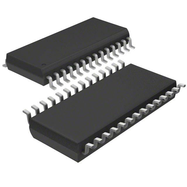
28-Pin TSSOP Package
KEY SPECIFICATIONS
•
•
•
•
•
•
•
Resolution: 10 Bits
Conversion Rate: 40 MSPS
Full Power Bandwidth: 400 MHz
DNL: ±0.3 LSB typ)
SNR (fIN = 11 MHz): 59.6 dB (typ)
SFDR (fIN = 11 MHz): -80 dB (typ)
Power Consumption, 40 MHz: 55.5 mW
APPLICATIONS
•
•
•
•
•
•
•
•
The differential inputs provide a full scale selectable
input swing of 2.0 VP-P, 1.5 VP-P, 1.0 VP-P, with the
possibility of a single-ended input. Full use of the
differential input is recommended for optimum
performance. An internal +1.2V precision bandgap
reference is used to set the ADC full-scale range, and
also allows the user to supply a buffered referenced
voltage for those applications requiring increased
accuracy. The output data format is user choice of
offset binary or two’s complement.
The ADC10040Q runs on an Automotive Grade Flow
and is AEC-Q100 Grade 3 Qualified.
This device is available in the 28-lead TSSOP
package and will operate over the industrial
temperature range of −40°C to +85°C.
Ultrasound and Imaging
Instrumentation
Cellular Base Stations/Communications
Receivers
Sonar/Radar
xDSL
Wireless Local Loops
Data Acquisition Systems
DSP Front Ends
1
2
Please be aware that an important notice concerning availability, standard warranty, and use in critical applications of
Texas Instruments semiconductor products and disclaimers thereto appears at the end of this data sheet.
All trademarks are the property of their respective owners.
PRODUCTION DATA information is current as of publication date.
Products conform to specifications per the terms of the Texas
Instruments standard warranty. Production processing does not
necessarily include testing of all parameters.
Copyright © 2003–2013, Texas Instruments Incorporated
�ADC10040
SNAS224M – JULY 2003 – REVISED APRIL 2013
www.ti.com
Connection Diagram
Figure 1. TSSOP Package
See Package Number PW0028A
Block Diagram
2
Submit Documentation Feedback
Copyright © 2003–2013, Texas Instruments Incorporated
Product Folder Links: ADC10040
�ADC10040
www.ti.com
SNAS224M – JULY 2003 – REVISED APRIL 2013
Pin Descriptions and Equivalent Circuits
Pin No.
Symbol
Equivalent Circuit
Description
ANALOG I/O
12
VIN−
Inverting analog input signal. With a 1.2V reference the full-scale
input signal level is a differential 1.0 VP-P. This pin may be tied to
VCOM (pin 4) for single-ended operation.
13
VIN+
Non-inverting analog input signal. With a 1.2V reference the fullscale input signal level is a differential 1.0 VP-P.
6
VREF
Reference Voltage. This device provides an internal 1.2V reference.
This pin should be bypassed to VSSA with a 0.1 µF monolithic
capacitor. VREF is 1.20V nominal. This pin may be driven by a 1.20V
external reference if desired. Do not load this pin.
7
VREFT
4
VCOM
8
VREFB
These pins are high impedance reference bypass pins only. Connect
a 0.1 µF capacitor from each of these pins to VSSA. These pins
should not be loaded. VCOM may be used to set the input common
mode voltage VCM.
DIGITAL I/O
1
CLK
15
DF
28
STBY
5
IRS (Input Range
Select)
Digital clock input. The range of frequencies for this input is 20 MHz
to 40 MHz. The input is sampled on the rising edge of this input.
DF = “1” Two’s Complement
DF = “0” Offset Binary
This is the standby pin. When high, this pin sets the converter into
standby mode. When this pin is low, the converter is in active mode.
IRS = “VDDA” 2.0 VP-P input range
IRS = “VSSA” 1.5 VP-P input range
IRS = “Floating” 1.0 VP-P input range
If using both VIN+ and VIN- pins, (or differential mode), then the
peak-to-peak voltage refers to the differential voltage (VIN+ - VIN-).
Submit Documentation Feedback
Copyright © 2003–2013, Texas Instruments Incorporated
Product Folder Links: ADC10040
3
�ADC10040
SNAS224M – JULY 2003 – REVISED APRIL 2013
www.ti.com
Pin Descriptions and Equivalent Circuits (continued)
Pin No.
Symbol
Equivalent Circuit
Description
16–20,
23–27
D0–D9
Digital output data. D0 is the LSB and D9 is the MSB of the binary
output word.
2, 9, 10
VDDA
Positive analog supply pins. These pins should be connected to a
quiet 3,0V source and bypassed to analog ground with a 0.1 µF
monolithic capacitor located within 1 cm of these pins. A 4.7 µF
capacitor should also be used in parallel.
3, 11, 14
VSSA
Ground return for the analog supply.
22
VDDIO
Positive digital supply pins for the ADC10040’s output drivers. This
pin should be bypassed to digital ground with a 0.1 µF monolithic
capacitor located within 1 cm of this pin. A 4.7 µF capacitor should
also be used in parallel. The voltage on this pin should never exceed
the voltage on VDDA by more than 300 mV.
21
VSSIO
The ground return for the digital supply for the output drivers. This
pin should be connected to the ground plane, but not near the
analog circuitry.
ANALOG POWER
DIGITAL POWER
These devices have limited built-in ESD protection. The leads should be shorted together or the device placed in conductive foam
during storage or handling to prevent electrostatic damage to the MOS gates.
4
Submit Documentation Feedback
Copyright © 2003–2013, Texas Instruments Incorporated
Product Folder Links: ADC10040
�ADC10040
www.ti.com
SNAS224M – JULY 2003 – REVISED APRIL 2013
Absolute Maximum Ratings (1) (2) (3)
VDDA, VDDIO
3.9V
−0.3V to VDDA or VDDIO
+0.3V
Voltage on Any Pin to GND
Input Current on Any Pin
±25 mA
(4)
±50 mA
Package Input Current
See (5)
Package Dissipation at T = 25°C
ESD Susceptibility
Human Body Model (6)
Machine Model
2500V
(6)
250V
Soldering Temperature Infrared, 10 sec. (7)
235°C
−65°C to +150°C
Storage Temperature
(1)
(2)
(3)
(4)
(5)
(6)
(7)
All voltages are measured with respect to GND = VSSA = VSSIO = 0V, unless otherwise specified.
Absolute Maximum Ratings indicate limits beyond which damage to the device may occur. Operating Ratings indicate conditions for
which the device is functional, but do not ensure specific performance limits. For ensured specifications and test conditions, see the
Electrical Characteristics. The ensured specifications apply only for the test conditions listed. Some performance characteristics may
degrade when the device is not operated under the listed test conditions.
If Military/Aerospace specified devices are required, please contact the Texas Instruments Sales Office/ Distributors for availability and
specifications.
When the voltage at any pin exceeds the power supplies (VIN < VSSA or VIN > VDDA), the current at that pin should be limited to 25 mA.
The 50 mA maximum package input current rating limits the number of pins that can safely exceed the power supplies with an input
current of 25 mA to two.
The absolute maximum junction temperature (TJmax) for this device is 150°C. The maximum allowable power dissipation is dictated by
TJmax, the junction-to-ambient thermal resistance (θJA), and the ambient temperature (TA), and can be calculated using the formula
PDMAX = (TJmax − TA)/θJA. In the 28-pin TSSOP, θJA is 96°C/W, so PDMAX = 1,302 mW at 25°C and 677 mW at the maximum
operating ambient temperature of 85°C. Note that the power dissipation of this device under normal operation will typically be about 55.5
mW. The values for maximum power dissipation listed above will be reached only when the ADC10040 is operated in a severe fault
condition.
Human body model is 100 pF capacitor discharged through a 1.5 kΩ resistor. Machine model is 220 pF discharged through 0Ω.
The 235°C reflow temperature refers to infrared reflow. For Vapor Phase Reflow (VPR) the following conditions apply: Maintain the
temperature at the top of the package body above 183°C for a minimum of 60 seconds. The temperature measured on the package
body must not exceed 220°C. Only one excursion above 183°C is allowed per reflow cycle.
Operating Ratings (1) (2)
−40°C ≤ TA ≤ +85°C
Operating Temperature Range
VDDA (Supply Voltage)
+2.7V to +3.6V
VDDIO (Output Driver Supply Voltage)
+2.5V to VDDA
VREF
1.20V
≤ 100 mV
|VSSA–VSSIO|
Clock Duty Cycle
(1)
(2)
30 to 70 %
Absolute Maximum Ratings indicate limits beyond which damage to the device may occur. Operating Ratings indicate conditions for
which the device is functional, but do not ensure specific performance limits. For ensured specifications and test conditions, see the
Electrical Characteristics. The ensured specifications apply only for the test conditions listed. Some performance characteristics may
degrade when the device is not operated under the listed test conditions.
All voltages are measured with respect to GND = VSSA = VSSIO = 0V, unless otherwise specified.
Submit Documentation Feedback
Copyright © 2003–2013, Texas Instruments Incorporated
Product Folder Links: ADC10040
5
�ADC10040
SNAS224M – JULY 2003 – REVISED APRIL 2013
www.ti.com
Converter Electrical Characteristics
Unless otherwise specified, the following specifications apply for VSSA = VSSIO = 0V, VDDA = +3.0V, VDDIO = +2.5V, VIN = 2 VP-P,
STBY = 0V, External VREF = 1.20V, fCLK = 40 MHz, 50% Duty Cycle, CL = 10 pF/pin. Boldface limits apply for TA = TMIN to
TMAX: all other limits TA = 25°C. (1) (2) (3)
Symbol
Parameter
Conditions
Min
Typ
Max
Units
STATIC CONVERTER CHARACTERISTICS
No Missing Codes Ensured
10
Bits
INL
Integral Non-Linearity
FIN = 250 kHz, −0 dB Full
Scale
−1.0
±0.3
+1.0
LSB
DNL
Differential Non-Linearity
FIN = 250 kHz, −0 dB Full
Scale
−0.9
±0.3
+0.9
LSB
GE
Gain Error
Positive Error
−1.5
+0.4
+1.9
% FS
Negative Error
−1.5
−0.01
+1.9
% FS
OE
Offset Error (VIN+ = VIN−)
−1.4
0.12
+1.6
% FS
FPBW
Under Range Output Code
0
Over Range Output Code
1023
Full Power Bandwidth (4)
400
MHz
REFERENCE AND INPUT CHARACTERISTICS
VCM
Common Mode Input Voltage
VCOM
Output Voltage for use as an input
common mode voltage (5)
1.45
V
VREF
Reference Voltage
1.2
V
Reference Voltage Temperature
Coefficient
±80
ppm/°C
4
pF
VREFTC
CIN
0.5
VIN Input Capacitance (each pin to
VSSA)
1.5
V
POWER SUPPLY CHARACTERISTICS
IVDDA
Analog Supply Current
IVDDIO
Digital Supply Current (6)
PWR
Power Consumption (7)
(1)
(2)
(3)
(4)
(5)
(6)
(7)
6
STBY = 1
4.5
6.0
mA
STBY = 0
18
25
mA
STBY = 1, fIN = 0 Hz
0
STBY = 0, fIN = 0 Hz
0.6
0.8
mA
STBY = 1
13.5
18
mW
STBY = 0
55.5
77
mW
mA
To ensure accuracy, it is required that |VDDA–VDDIO| ≤ 100 mV and separate bypass capacitors are used at each power supply pin.
With the test condition for 2 VP-P differential input, the 10-bit LSB is 1.95 mV.
Typical figures are at TA = TJ = 25°C and represent most likely parametric norms. Test limits are ensured to TI's AOQL (Average
Outgoing Quality Level).
The input bandwidth is limited using a capacitor between VIN− and VIN+.
VCOM is a typical value, measured at room temperature. It is not ensured by test. Do not load this pin.
VDDIO is the current consumed by the switching of the output drivers and is primarily determined by load capacitance on the output pins,
the supply voltage, VDR, and the rate at which the outputs are switching (which is signal dependent). IDR = VDR x (C0 x f0 + C1 x f1 + C2
+ f2 +....C11 x f11) where VDR is the output driver supply voltage, Cn is the total load capacitance on the output pin, and fn is the average
frequency at which the pin is toggling.
Power consumption includes output driver power. (fIN = 0 MHz).
Submit Documentation Feedback
Copyright © 2003–2013, Texas Instruments Incorporated
Product Folder Links: ADC10040
�ADC10040
www.ti.com
SNAS224M – JULY 2003 – REVISED APRIL 2013
DC and Logic Electrical Characteristics
Unless otherwise specified, the following specifications apply for VSSA = VSSIO = 0V, VDDA = +3.0V, VDDIO = +2.5V, VIN = 2 VP-P,
STBY = 0V, External VREF = 1.20V, fCLK = 40 MHz, 50% Duty Cycle, CL = 10 pF/pin. Boldface limits apply for TA = TMIN to
TMAX: all other limits TA = 25°C (1) (2) (3)
Symbol
Parameter
Conditions
Min
Typ
Max
Units
CLK, DF, STBY, SENSE
Logical “1” Input Voltage
2
V
Logical “0” Input Voltage
0.8
V
Logical “1” Input Current
+10
µA
−10
Logical “0” Input Current
µA
D0–D9 OUTPUT CHARACTERISTICS
Logical “1” Output Voltage
IOUT = −0.5 mA
Logical “0” Output Voltage
IOUT = 1.6 mA
VDDIO − 0.2
V
0.4
V
DYNAMIC CONVERTER CHARACTERISTICS (4)
ENOB
SNR
SINAD
2nd HD
3rd HD
THD
SFDR
(1)
(2)
(3)
(4)
fIN = 11 MHz
9.4,
9.3
9.6
Bits
fIN = 19 MHz
9.4,
9.3
9.6
Bits
fIN = 11 MHz
58.7,
58.1
59.6
dB
fIN = 19 MHz
58.6,
58
59.5
dB
fIN = 11 MHz
58.6,
58
59.5
fIN = 19 MHz
58.5,
57.8
59.4
fIN = 11 MHz
−75.9,
−74.7
−89
dBc
fIN = 19 MHz
−74.4,
−73
−86
dBc
fIN = 11 MHz
−69.5,
−67.5
−78
dBc
fIN = 19 MHz
−68.8,
−66.7
−77
dBc
fIN = 11 MHz
−69.5,
−67.5
−78
dB
f.IN = 19 MHz
−68.8,
−66.7
−77
dB
fIN = 11 MHz
−75.8,
−74.5
−80
dBc
fIN = 19 MHz
−75.7,
−74.3
−80
dBc
Effective Number of Bits
Signal-to-Noise Ratio
Signal-to-Noise Ratio + Distortion
2nd Harmonic
3rd Harmonic
Total Harmonic Distortion (First 6
Harmonics)
Spurious Free Dynamic Range
(Excluding 2nd and 3rd Harmonic)
dB
dB
To ensure accuracy, it is required that |VDDA–VDDIO| ≤ 100 mV and separate bypass capacitors are used at each power supply pin.
With the test condition for 2 VP-P differential input, the 10-bit LSB is 1.95 mV.
Typical figures are at TA = TJ = 25°C and represent most likely parametric norms. Test limits are ensured to TI's AOQL (Average
Outgoing Quality Level).
Optimum dynamic performance will be obtained by keeping the reference input in the +1.2V.
Submit Documentation Feedback
Copyright © 2003–2013, Texas Instruments Incorporated
Product Folder Links: ADC10040
7
�ADC10040
SNAS224M – JULY 2003 – REVISED APRIL 2013
www.ti.com
AC Electrical Characteristics
Unless otherwise specified, the following specifications apply for VSSA = VSSIO = 0V, VDDA = +3.0V, VDDIO = +2.5V, VIN = 2 VP-P
(full scale), STBY = 0V, External VREF = 1.20V, fCLK = 40 MHz, 50% Duty Cycle, CL = 10 pF/pin. Boldface limits apply for TA
= TMIN to TMAX: all other limits TA = 25°C (1) (2) (3)
Symbol
Parameter
Conditions
Min (3)
Typ (3)
Max (3)
Units
40
MHz (min)
CLK, DF, STBY, SENSE
fCLK1
Maximum Clock Frequency
fCLK2
Minimum Clock Frequency
20
MHz
tCH
Clock High Time
12.5
ns
tCL
Clock Low Time
12.5
ns
tCONV
Conversion Latency
tOD
Data Output Delay after a Rising Clock
Edge
tAD
Aperture Delay
tAJ
Aperture Jitter
Over Range Recovery Time
tSTBY
(1)
(2)
(3)
8
T = 25°C
2
3.3
1
Differential VIN step from ±3V
to 0V to get accurate
conversion
Standby Mode Exit Cycle
6
Cycles
5
ns
6
ns
1
ns
2
ps (RMS)
1
Clock Cycle
20
Cycles
With the test condition for 2 VP-P differential input, the 10-bit LSB is 1.95 mV.
Typical figures are at TA = TJ = 25°C and represent most likely parametric norms. Test limits are ensured to TI's AOQL (Average
Outgoing Quality Level).
Timing specifications are tested at TTL logic levels, VIL = 0.4V for a falling edge, and VIH = 2.4V for a rising edge.
Submit Documentation Feedback
Copyright © 2003–2013, Texas Instruments Incorporated
Product Folder Links: ADC10040
�ADC10040
www.ti.com
SNAS224M – JULY 2003 – REVISED APRIL 2013
Specification Definitions
APERTURE DELAY is the time after the rising edge of the clock to when the input signal is acquired or held for
conversion.
APERTURE JITTER (APERTURE UNCERTAINTY) is the variation in aperture delay from sample to sample.
Aperture jitter manifests itself as noise in the output.
COMMON MODE VOLTAGE (VCM) is the d.c. potential present at both signal inputs to the ADC.
CONVERSION LATENCY See PIPELINE DELAY.
DIFFERENTIAL NON-LINEARITY (DNL) is the measure of the maximum deviation from the ideal step size of 1
LSB.
DUTY CYCLE is the ratio of the time that a repetitive digital waveform is high to the total time of one period. The
specification here refers to the ADC clock input signal.
EFFECTIVE NUMBER OF BITS (ENOB, or EFFECTIVE BITS) is another method of specifying Signal-to-Noise
and Distortion or SINAD. ENOB is defined as (SINAD - 1.76) / 6.02 and states that the converter is equivalent to
a perfect ADC of this (ENOB) number of bits.
FULL POWER BANDWIDTH is a measure of the frequency at which the reconstructed output fundamental
drops 3 dB below its low frequency value for a full scale input.
GAIN ERROR is the deviation from the ideal slope of the transfer function. It can be calculated as:
Gain Error = Pos. Full-Scale Error − Neg. Full-Scale Error
(1)
INTEGRAL NON LINEARITY (INL) is a measure of the deviation of each individual code from a line drawn from
negative full scale through positive full scale. The deviation of any given code from this straight line is measured
from the center of that code value.
MISSING CODES are those output codes that will never appear at the ADC outputs. The ADC10040 is ensured
not to have any missing codes.
NEGATIVE FULL SCALE ERROR is the difference between the input voltage (VIN+ − VIN−) just causing a
transition from negative full scale to the first code and its ideal value of 0.5 LSB.
OFFSET ERROR is the input voltage that will cause a transition from a code of 01 1111 1111 to a code of 10
0000 0000.
OUTPUT DELAY is the time delay after the rising edge of the clock before the data update is presented at the
output pins.
PIPELINE DELAY (LATENCY) is the number of clock cycles between initiation of conversion and when that data
is presented to the output driver stage. Data for any given sample is available at the output pins the Pipeline
Delay plus the Output Delay after the sample is taken. New data is available at every clock cycle, but the data
lags the conversion by the pipeline delay.
POSITIVE FULL SCALE ERROR is the difference between the actual last code transition and its ideal value of
1½ LSB below positive full scale.
SIGNAL TO NOISE RATIO (SNR) is the ratio, expressed in dB, of the rms value of the input signal to the rms
value of the sum of all other spectral components below one-half the sampling frequency, not including
harmonics or DC.
SIGNAL TO NOISE PLUS DISTORTION (S/N+D or SINAD) Is the ratio, expressed in dB, of the rms value of the
input signal to the rms value of all of the other spectral components below half the clock frequency, including
harmonics but excluding d.c.
SPURIOUS FREE DYNAMIC RANGE (SFDR) is the difference, expressed in dB, between the rms values of the
input signal and the peak spurious signal, where a spurious signal is any signal present in the output spectrum
that is not present at the input.
Submit Documentation Feedback
Copyright © 2003–2013, Texas Instruments Incorporated
Product Folder Links: ADC10040
9
�ADC10040
SNAS224M – JULY 2003 – REVISED APRIL 2013
www.ti.com
TOTAL HARMONIC DISTORTION (THD) is the ratio, expressed in dBc, of the rms total of the first six harmonic
levels at the output to the level of the fundamental at the output. THD is calculated as:
(2)
where f1 is the RMS power of the fundamental (output) frequency and f2 through f6 are the RMS power in the first
6 harmonic frequencies.
SECOND HARMONIC DISTORTION (2ND HARM) is the difference expressed in dB, between the RMS power in
the input frequency at the output and the power in its 2nd harmonic level at the output.
THIRD HARMONIC DISTORTION (3RD HARM) is the difference, expressed in dB, between the RMS power in
the input frequency at the output and the power in its 3rd harmonic level at the output.
Timing Diagram
Figure 2. Clock and Data Timing Diagram
Transfer Characteristics
Figure 3. Input vs. Output Transfer Characteristic
10
Submit Documentation Feedback
Copyright © 2003–2013, Texas Instruments Incorporated
Product Folder Links: ADC10040
�ADC10040
www.ti.com
SNAS224M – JULY 2003 – REVISED APRIL 2013
Typical Performance Characteristics
Unless otherwise specified, the following specifications apply: VSSA = VSSIO = 0V, VDDA = +3.0V, VDDIO = +2.5V, VIN = 2 VP-P,
STBY = 0V, External VREF = 1.2V, fCLK = 40 MHz, fIN = 19 MHz, 50% Duty Cycle.
Figure 4. DNL
Figure 5. DNL vs. fCLK
Figure 6. DNL vs. Clock Duty Cycle (DC input)
Figure 7. DNL vs. Temperature
Figure 8. INL
Figure 9. INL vs. fCLK
Submit Documentation Feedback
Copyright © 2003–2013, Texas Instruments Incorporated
Product Folder Links: ADC10040
11
�ADC10040
SNAS224M – JULY 2003 – REVISED APRIL 2013
www.ti.com
Typical Performance Characteristics (continued)
Unless otherwise specified, the following specifications apply: VSSA = VSSIO = 0V, VDDA = +3.0V, VDDIO = +2.5V, VIN = 2 VP-P,
STBY = 0V, External VREF = 1.2V, fCLK = 40 MHz, fIN = 19 MHz, 50% Duty Cycle.
12
Figure 10. INL vs. Clock Duty Cycle
Figure 11. SNR vs. VDDIO
Figure 12. SNR vs. VDDA
Figure 13. SNR vs. fCLK
Figure 14. INL vs. Temperature
Figure 15. SNR vs. Clock Duty Cycle
Submit Documentation Feedback
Copyright © 2003–2013, Texas Instruments Incorporated
Product Folder Links: ADC10040
�ADC10040
www.ti.com
SNAS224M – JULY 2003 – REVISED APRIL 2013
Typical Performance Characteristics (continued)
Unless otherwise specified, the following specifications apply: VSSA = VSSIO = 0V, VDDA = +3.0V, VDDIO = +2.5V, VIN = 2 VP-P,
STBY = 0V, External VREF = 1.2V, fCLK = 40 MHz, fIN = 19 MHz, 50% Duty Cycle.
Figure 16. SNR vs. Temperature
Figure 17. THD vs. VDDA
Figure 18. THD vs. VDDIO
Figure 19. THD vs. fCLK
Figure 20. SNR vs. IRS
Figure 21. THD vs. IRS
Submit Documentation Feedback
Copyright © 2003–2013, Texas Instruments Incorporated
Product Folder Links: ADC10040
13
�ADC10040
SNAS224M – JULY 2003 – REVISED APRIL 2013
www.ti.com
Typical Performance Characteristics (continued)
Unless otherwise specified, the following specifications apply: VSSA = VSSIO = 0V, VDDA = +3.0V, VDDIO = +2.5V, VIN = 2 VP-P,
STBY = 0V, External VREF = 1.2V, fCLK = 40 MHz, fIN = 19 MHz, 50% Duty Cycle.
14
Figure 22. SINAD vs. VDDA
Figure 23. SINAD vs. VDDIO
Figure 24. THD vs. Clock Duty Cycle
Figure 25. SINAD vs. Clock Duty Cycle
Figure 26. THD vs. Temperature
Figure 27. SINAD vs. Temperature
Submit Documentation Feedback
Copyright © 2003–2013, Texas Instruments Incorporated
Product Folder Links: ADC10040
�ADC10040
www.ti.com
SNAS224M – JULY 2003 – REVISED APRIL 2013
Typical Performance Characteristics (continued)
Unless otherwise specified, the following specifications apply: VSSA = VSSIO = 0V, VDDA = +3.0V, VDDIO = +2.5V, VIN = 2 VP-P,
STBY = 0V, External VREF = 1.2V, fCLK = 40 MHz, fIN = 19 MHz, 50% Duty Cycle.
Figure 28. SINAD vs. fCLK
Figure 29. SFDR vs. VDDIO
Figure 30. SINAD vs. IRS
Figure 31. SFDR vs. fCLK
Figure 32. SFDR vs. VDDA
Figure 33. SFDR vs. IRS
Submit Documentation Feedback
Copyright © 2003–2013, Texas Instruments Incorporated
Product Folder Links: ADC10040
15
�ADC10040
SNAS224M – JULY 2003 – REVISED APRIL 2013
www.ti.com
Typical Performance Characteristics (continued)
Unless otherwise specified, the following specifications apply: VSSA = VSSIO = 0V, VDDA = +3.0V, VDDIO = +2.5V, VIN = 2 VP-P,
STBY = 0V, External VREF = 1.2V, fCLK = 40 MHz, fIN = 19 MHz, 50% Duty Cycle.
16
Figure 34. SFDR vs. Clock Duty Cycle
Figure 35. Spectral Response @ 11 MHz Input
Figure 36. SFDR vs. Temperature
Figure 37. Spectral Response @ 19 MHz Input
Submit Documentation Feedback
Copyright © 2003–2013, Texas Instruments Incorporated
Product Folder Links: ADC10040
�ADC10040
www.ti.com
SNAS224M – JULY 2003 – REVISED APRIL 2013
FUNCTIONAL DESCRIPTION
The ADC10040 uses a pipeline architecture and has error correction circuitry to help ensure maximum
performance. Differential analog input signals are digitized to 10 bits. In differential mode , each analog input
signal should have a peak-to-peak voltage equal to 1.0V, 0.75V or 0.5V, depending on the state of the IRS pin
(pin 5), and be centered around VCM and be 180° out of phase with each other. If single ended operation is
desired, VIN- may be tied to the VCOM pin (pin 4). A single ended input signal may then be applied to VIN+, and
should have an average value in the range of VCM. The signal amplitude should be 2.0V, 1.5V or 1.0V peak-topeak, depending on the state or the IRS pin (pin 5).
APPLICATIONS INFORMATION
ANALOG INPUTS
The ADC10040 has two analog signal inputs, VIN+ and VIN−. These two pins form a differential input pair. There
is one common mode pin VCOM that may be used to set the common mode input voltage.
REFERENCE PINS
The ADC10040 is designed to operate with an internal or external 1.2V reference. The internal 1.2V reference is
the defualt condition. If an external voltage is applied to the VREF pin, then that voltage is used for the reference.
The VREF pin should be bypassed to ground with a 0.1 µF capacitor placed close to the pin. Do not load this pin
when using the internal reference.
The voltages at VCOM, VREFT, and VREFB are derived from the reference voltage. These pins are made available
for bypass purposes only. These pins should each be bypassed to ground with a 0.1 µF capacitor placed close
to the pin. It is very important that all grounds associated with the reference voltage and the input signal make
connection to the analog ground plane at a single point to minimize the effects of noise currents in the ground
path. DO NOT LOAD these pins.
VCOM PIN
This pin supplies a voltage for possible use to set the common mode input voltage. This pin may also be
connected to VIN-, so that VIN+ may be used as a single ended input. These pins should be bypassed with at
least a 0.1uF capacitor. Do not load this pin.
SIGNAL INPUTS
The signal inputs are VIN+ and VIN−. The input signal amplitude is defined as VIN+ − VIN− and is represented
schematically in Figure 38:
2.5V Max
VCM + 0.5V
VCM
VCM - 0.5V
0V Min
Figure 38. Input Voltage Waveforms for a 2VP-P differential Input
Submit Documentation Feedback
Copyright © 2003–2013, Texas Instruments Incorporated
Product Folder Links: ADC10040
17
�ADC10040
SNAS224M – JULY 2003 – REVISED APRIL 2013
www.ti.com
2.5V Max
VCM + 1V
VCM
VCM - 1V
0V Min
Figure 39. Input Voltage Waveform for a 2VP-P Single Ended Input
A single ended input signal is shown in Figure 39.
The internal switching action at the analog inputs causes energy to be output from the input pins. As the driving
source tries to compensate for this, it adds noise to the signal. To minimize the effects of this, use 18Ω series
resistors at each of the signal inputs with a 25 pF capacitor across the inputs, as shown in Figure 40. These
components should be placed close to the ADC because the input pins of the ADC is the most sensitive part of
the system and this is the last opportunity to filter the input. The two 16Ω resistors and the 24 pF capacitor,
together with the 4 pF ADC input capacitance, form a low-pass filter with a -3 dB frequency of 177 MHz.
CLK PIN
The CLK signal controls the timing of the sampling process. Drive the clock input with a stable, low jitter clock
signal in the frequency range indicated in the AC Electrical Characteristics Table with rise and fall times of less
than 2 ns. The trace carrying the clock signal should be as short as possible and should not cross any other
signal line, analog or digital, not even at 90°. The CLK signal also drives an internal state machine. If the CLK is
interrupted, or its frequency is too low, the charge on internal capacitors can dissipate to the point where the
accuracy of the output data will degrade. This is what limits the lowest sample rate. The duty cycle of the clock
signal can affect the performance of any A/D Converter. Because achieving a precise duty cycle is difficult, the
ADC10040 is designed to maintain performance over a range of duty cycles. While it is specified and
performance is ensured with a 50% clock duty cycle, performance is typically maintained with minimum clock low
and high times indicated in the AC Electrical Characteristics Table. Both minimum high and low times may not be
held simultaneously.
STBY PIN
The STBY pin, when high, holds the ADC10040 in a power-down mode to conserve power when the converter is
not being used. The power consumption in this state is 13.5 mW. The output data pins are undefined in this
mode. Power consumption during power-down is not affected by the clock frequency, or by whether there is a
clock signal present. The data in the pipeline is corrupted while in the power down.
DF PIN
The DF (Data Format) pin, when high, forces the ADC10040 to output the 2’s complement data format. When DF
is tied low, the output format is offset binary.
IRS PIN
The IRS (Input Range Select) pin defines the input signal amplitude that will produce a full scale output. The
table below describes the function of the IRS pin.
Table 1. IRS Pin Functions
18
IRS Pin
Full-Scale Input
VDDA
2.0VP-P
VSSA
1.5VP-P
Floating
1.0VP-P
Submit Documentation Feedback
Copyright © 2003–2013, Texas Instruments Incorporated
Product Folder Links: ADC10040
�ADC10040
www.ti.com
SNAS224M – JULY 2003 – REVISED APRIL 2013
OUTPUT PINS
The ADC10040 has 10 TTL/CMOS compatible Data Output pins. The offset binary data is present at these
outputs while the DF and STBY pins are low. Be very careful when driving a high capacitance bus. The more
capacitance the output drivers must charge for each conversion, the more instantaneous digital current flows
through VDDIO and VSSIO. These large charging current spikes can cause on-chip noise and couple into the
analog circuitry, degrading dynamic performance. Adequate bypassing, limiting output capacitance and careful
attention to the ground plane will reduce this problem. Additionally, bus capacitance beyond the specified 10
pF/pin will cause tOD to increase, making it difficult to properly latch the ADC output data. The result could be an
apparent reduction in dynamic performance. To minimize noise due to output switching, minimize the load
currents at the digital outputs. This can be done by minimizing load capacitance and by connecting buffers
between the ADC outputs and any other circuitry, which will isolate the outputs from trace and other circuit
capacitances and limit the output currents, which could otherwise result in performance degradation. Only one
driven input should be connected to the ADC output pins.
While the tOD time provides information about output timing, a simple way to capture a valid output is to latch the
data on the rising edge of the conversion clock.
APPLICATION SCHEMATICS
The following figures show simple examples of using the ADC10040. The ADC10040 performs best with a
differential input signal.
Narrow Band A.C. Signals
Figure 40 shows a typical circuit for an AC coupled, differentially driven input. The 16Ω resistors and 24 pF
capacitor, together with the 4 pF input capacitance of the ADC10040, provides a −3dB input bandwidth of 177
MHz, while the 0.1µF capacitor at VCOM stabilizes the common move voltage at the transformer center tap.
VDDIO
1
7
VCC
VCC 18
VCC 31
VCC 42
4 OE
3 OE
25
2 OE
48
1 OE
24
26
4A3
29
4A2
30
4A1
VDDIO
AIN
12
4
VDDA 22
10
D1
D2
D3
VIN-
VCOM
24 pF
13
D0
VIN+
16:
D4
D5
D6
D7
D8
D9
0.1 PF
VSSA
14
VSSA
24
23
20
19
18
17
16
15
28
3A4
3A3
35
3A2
36
3A1
33
37
2A4
38
2A3
40
2A2
41
2A1
43
1A4
44 1A3
46
1A2
47 1A1
3Y4 17
3Y3 16
14
3Y2
13
3Y1
D0
CLKOUT
D1
12
2Y4
11
2Y3
9
2Y2
8
2Y1
D2
6
1Y4
5
1Y3
1Y2 3
2
1Y1
D6
D7
D3
D4
D5
D8
D9
21
3
0.1 PF
11
0.1 PF
VSSA
VREF
VREFT
8
VREFB
7
26
25
VSSIO
DF
STBY
6
27
CLKIN
4Y4 23
4Y3 22
4Y2 20
19
4Y1
4
GND
10
GND
15
GND
21
GND
28
GND
34
GND
39
GND
45
GND
16:
4.7 PF
IRS
CLK
32
0.1 PF
ADC10040
1
CLKIN
VDDA
VDDA
5
9
0.1 PF
4.7 PF
VDDA
2
VDDA
74ACTQ16244
27
0.1 PF
Figure 40. A Simple Application Using a Differential Signal Source
Submit Documentation Feedback
Copyright © 2003–2013, Texas Instruments Incorporated
Product Folder Links: ADC10040
19
�ADC10040
SNAS224M – JULY 2003 – REVISED APRIL 2013
www.ti.com
D.C. Applications
For very low frequency and DC input applications, a d.c. coupled amplifier or buffer may be needed, especially
when the input is single-ended and the advantages of a differential input signal is desired. Figure 41 shows the
input drive circuit that can be used to replace the transformer of Figure 40. The LMH6550 provides excellent
performance and is well-suited for this application. The common mode output voltage of the LMH6550 is the
same as its VCM input.
RF
RT
RG
16:
VCM
LMH6550
ADC
Input
24 pF
+
RT
RG
50:
16:
50:
From
ADC
RF
VCOM
Figure 41. Using the LMH6550 for DC and wideband applications
Single Ended Applications
Performance of the ADC10040 with a single-ended input is not as good as its performance with a differential
input. However, if the lower performance is adequate, the circuit of Figure 42 shows an acceptable method of
driving the analog input.
VDDIO
1
7
VCC
VCC 18
VCC 31
VCC 42
4 OE
3 OE
25
2 OE
48
1 OE
24
26
4A3
29
4A2
30
4A1
VDDIO
CLK
VIN-
AIN
13
VCOM
VIN+
51 pF
D4
D5
D6
D7
D8
D9
DF
STBY
VSSA
14
3
0.1 PF
VSSA
0.1 PF
11
V
7 REF
VREFT
8
VREFB
VSSA
6
27
26
25
24
23
20
19
18
17
16
15
28
3A4
3A3
35
3A2
36
3A1
33
37
2A4
38
2A3
40
2A2
41
2A1
43
1A4
44 1A3
46
1A2
47 1A1
3Y4 17
3Y3 16
14
3Y2
13
3Y1
D0
CLKOUT
D1
12
2Y4
11
2Y3
9
2Y2
8
2Y1
D2
6
1Y4
5
1Y3
1Y2 3
2
1Y1
D6
D7
D3
D4
D5
D8
D9
4
GND
10
GND
15
GND
21
GND
28
GND
34
GND
39
GND
45
GND
16:
VDDA 22
10
D1
D2
D3
IRS
0.1 PF
4
D0
CLKIN
VSSIO
12
4.7 PF
4Y4 23
4Y3 22
4Y2 20
19
4Y1
21
1
CLKIN
32
0.1 PF
ADC10040
5
VDDA
VDDA
9
0.1 PF
4.7 PF
VDDA
2
VDDA
74ACTQ16244
27
0.1 PF
Figure 42. A Simple Application Using a Single Ended Signal Source
20
Submit Documentation Feedback
Copyright © 2003–2013, Texas Instruments Incorporated
Product Folder Links: ADC10040
�ADC10040
www.ti.com
SNAS224M – JULY 2003 – REVISED APRIL 2013
REVISION HISTORY
Changes from Revision L (April 2013) to Revision M
•
Page
Changed layout of National Data Sheet to TI format .......................................................................................................... 20
Submit Documentation Feedback
Copyright © 2003–2013, Texas Instruments Incorporated
Product Folder Links: ADC10040
21
�PACKAGE OPTION ADDENDUM
www.ti.com
13-Sep-2014
PACKAGING INFORMATION
Orderable Device
Status
(1)
Package Type Package Pins Package
Drawing
Qty
Eco Plan
Lead/Ball Finish
MSL Peak Temp
(2)
(6)
(3)
Op Temp (°C)
Device Marking
(4/5)
ADC10040CIMT/NOPB
ACTIVE
TSSOP
PW
28
48
Green (RoHS
& no Sb/Br)
CU SN
Level-3-260C-168 HR
-40 to 85
ADC10040
CIMT
ADC10040CIMTX/NOPB
ACTIVE
TSSOP
PW
28
2500
Green (RoHS
& no Sb/Br)
CU SN
Level-3-260C-168 HR
-40 to 85
ADC10040
CIMT
ADC10040QCIMT/NOPB
ACTIVE
TSSOP
PW
28
48
Green (RoHS
& no Sb/Br)
CU SN
Level-3-260C-168 HR
-40 to 85
ADC10040
QCIMT
ADC10040QCIMTX/NOPB
ACTIVE
TSSOP
PW
28
2500
Green (RoHS
& no Sb/Br)
CU SN
Level-3-260C-168 HR
-40 to 85
ADC10040
QCIMT
(1)
The marketing status values are defined as follows:
ACTIVE: Product device recommended for new designs.
LIFEBUY: TI has announced that the device will be discontinued, and a lifetime-buy period is in effect.
NRND: Not recommended for new designs. Device is in production to support existing customers, but TI does not recommend using this part in a new design.
PREVIEW: Device has been announced but is not in production. Samples may or may not be available.
OBSOLETE: TI has discontinued the production of the device.
(2)
Eco Plan - The planned eco-friendly classification: Pb-Free (RoHS), Pb-Free (RoHS Exempt), or Green (RoHS & no Sb/Br) - please check http://www.ti.com/productcontent for the latest availability
information and additional product content details.
TBD: The Pb-Free/Green conversion plan has not been defined.
Pb-Free (RoHS): TI's terms "Lead-Free" or "Pb-Free" mean semiconductor products that are compatible with the current RoHS requirements for all 6 substances, including the requirement that
lead not exceed 0.1% by weight in homogeneous materials. Where designed to be soldered at high temperatures, TI Pb-Free products are suitable for use in specified lead-free processes.
Pb-Free (RoHS Exempt): This component has a RoHS exemption for either 1) lead-based flip-chip solder bumps used between the die and package, or 2) lead-based die adhesive used between
the die and leadframe. The component is otherwise considered Pb-Free (RoHS compatible) as defined above.
Green (RoHS & no Sb/Br): TI defines "Green" to mean Pb-Free (RoHS compatible), and free of Bromine (Br) and Antimony (Sb) based flame retardants (Br or Sb do not exceed 0.1% by weight
in homogeneous material)
(3)
MSL, Peak Temp. - The Moisture Sensitivity Level rating according to the JEDEC industry standard classifications, and peak solder temperature.
(4)
There may be additional marking, which relates to the logo, the lot trace code information, or the environmental category on the device.
(5)
Multiple Device Markings will be inside parentheses. Only one Device Marking contained in parentheses and separated by a "~" will appear on a device. If a line is indented then it is a continuation
of the previous line and the two combined represent the entire Device Marking for that device.
(6)
Lead/Ball Finish - Orderable Devices may have multiple material finish options. Finish options are separated by a vertical ruled line. Lead/Ball Finish values may wrap to two lines if the finish
value exceeds the maximum column width.
Addendum-Page 1
Samples
�PACKAGE OPTION ADDENDUM
www.ti.com
13-Sep-2014
Important Information and Disclaimer:The information provided on this page represents TI's knowledge and belief as of the date that it is provided. TI bases its knowledge and belief on information
provided by third parties, and makes no representation or warranty as to the accuracy of such information. Efforts are underway to better integrate information from third parties. TI has taken and
continues to take reasonable steps to provide representative and accurate information but may not have conducted destructive testing or chemical analysis on incoming materials and chemicals.
TI and TI suppliers consider certain information to be proprietary, and thus CAS numbers and other limited information may not be available for release.
In no event shall TI's liability arising out of such information exceed the total purchase price of the TI part(s) at issue in this document sold by TI to Customer on an annual basis.
OTHER QUALIFIED VERSIONS OF ADC10040, ADC10040-Q1 :
• Catalog: ADC10040
• Automotive: ADC10040-Q1
NOTE: Qualified Version Definitions:
• Catalog - TI's standard catalog product
• Automotive - Q100 devices qualified for high-reliability automotive applications targeting zero defects
Addendum-Page 2
�PACKAGE MATERIALS INFORMATION
www.ti.com
23-Sep-2013
TAPE AND REEL INFORMATION
*All dimensions are nominal
Device
ADC10040CIMTX/NOPB
Package Package Pins
Type Drawing
SPQ
Reel
Reel
A0
Diameter Width (mm)
(mm) W1 (mm)
B0
(mm)
K0
(mm)
P1
(mm)
W
Pin1
(mm) Quadrant
TSSOP
PW
28
2500
330.0
16.4
6.8
10.2
1.6
8.0
16.0
Q1
ADC10040QCIMTX/NOPB TSSOP
PW
28
2500
330.0
16.4
6.8
10.2
1.6
8.0
16.0
Q1
Pack Materials-Page 1
�PACKAGE MATERIALS INFORMATION
www.ti.com
23-Sep-2013
*All dimensions are nominal
Device
Package Type
Package Drawing
Pins
SPQ
Length (mm)
Width (mm)
Height (mm)
ADC10040CIMTX/NOPB
TSSOP
PW
28
2500
367.0
367.0
38.0
ADC10040QCIMTX/NOPB
TSSOP
PW
28
2500
367.0
367.0
38.0
Pack Materials-Page 2
��IMPORTANT NOTICE
Texas Instruments Incorporated and its subsidiaries (TI) reserve the right to make corrections, enhancements, improvements and other
changes to its semiconductor products and services per JESD46, latest issue, and to discontinue any product or service per JESD48, latest
issue. Buyers should obtain the latest relevant information before placing orders and should verify that such information is current and
complete. All semiconductor products (also referred to herein as “components”) are sold subject to TI’s terms and conditions of sale
supplied at the time of order acknowledgment.
TI warrants performance of its components to the specifications applicable at the time of sale, in accordance with the warranty in TI’s terms
and conditions of sale of semiconductor products. Testing and other quality control techniques are used to the extent TI deems necessary
to support this warranty. Except where mandated by applicable law, testing of all parameters of each component is not necessarily
performed.
TI assumes no liability for applications assistance or the design of Buyers’ products. Buyers are responsible for their products and
applications using TI components. To minimize the risks associated with Buyers’ products and applications, Buyers should provide
adequate design and operating safeguards.
TI does not warrant or represent that any license, either express or implied, is granted under any patent right, copyright, mask work right, or
other intellectual property right relating to any combination, machine, or process in which TI components or services are used. Information
published by TI regarding third-party products or services does not constitute a license to use such products or services or a warranty or
endorsement thereof. Use of such information may require a license from a third party under the patents or other intellectual property of the
third party, or a license from TI under the patents or other intellectual property of TI.
Reproduction of significant portions of TI information in TI data books or data sheets is permissible only if reproduction is without alteration
and is accompanied by all associated warranties, conditions, limitations, and notices. TI is not responsible or liable for such altered
documentation. Information of third parties may be subject to additional restrictions.
Resale of TI components or services with statements different from or beyond the parameters stated by TI for that component or service
voids all express and any implied warranties for the associated TI component or service and is an unfair and deceptive business practice.
TI is not responsible or liable for any such statements.
Buyer acknowledges and agrees that it is solely responsible for compliance with all legal, regulatory and safety-related requirements
concerning its products, and any use of TI components in its applications, notwithstanding any applications-related information or support
that may be provided by TI. Buyer represents and agrees that it has all the necessary expertise to create and implement safeguards which
anticipate dangerous consequences of failures, monitor failures and their consequences, lessen the likelihood of failures that might cause
harm and take appropriate remedial actions. Buyer will fully indemnify TI and its representatives against any damages arising out of the use
of any TI components in safety-critical applications.
In some cases, TI components may be promoted specifically to facilitate safety-related applications. With such components, TI’s goal is to
help enable customers to design and create their own end-product solutions that meet applicable functional safety standards and
requirements. Nonetheless, such components are subject to these terms.
No TI components are authorized for use in FDA Class III (or similar life-critical medical equipment) unless authorized officers of the parties
have executed a special agreement specifically governing such use.
Only those TI components which TI has specifically designated as military grade or “enhanced plastic” are designed and intended for use in
military/aerospace applications or environments. Buyer acknowledges and agrees that any military or aerospace use of TI components
which have not been so designated is solely at the Buyer's risk, and that Buyer is solely responsible for compliance with all legal and
regulatory requirements in connection with such use.
TI has specifically designated certain components as meeting ISO/TS16949 requirements, mainly for automotive use. In any case of use of
non-designated products, TI will not be responsible for any failure to meet ISO/TS16949.
Products
Applications
Audio
www.ti.com/audio
Automotive and Transportation
www.ti.com/automotive
Amplifiers
amplifier.ti.com
Communications and Telecom
www.ti.com/communications
Data Converters
dataconverter.ti.com
Computers and Peripherals
www.ti.com/computers
DLP® Products
www.dlp.com
Consumer Electronics
www.ti.com/consumer-apps
DSP
dsp.ti.com
Energy and Lighting
www.ti.com/energy
Clocks and Timers
www.ti.com/clocks
Industrial
www.ti.com/industrial
Interface
interface.ti.com
Medical
www.ti.com/medical
Logic
logic.ti.com
Security
www.ti.com/security
Power Mgmt
power.ti.com
Space, Avionics and Defense
www.ti.com/space-avionics-defense
Microcontrollers
microcontroller.ti.com
Video and Imaging
www.ti.com/video
RFID
www.ti-rfid.com
OMAP Applications Processors
www.ti.com/omap
TI E2E Community
e2e.ti.com
Wireless Connectivity
www.ti.com/wirelessconnectivity
Mailing Address: Texas Instruments, Post Office Box 655303, Dallas, Texas 75265
Copyright © 2014, Texas Instruments Incorporated
�


 工商网监
湘ICP备2023018690号
工商网监
湘ICP备2023018690号
