User's Guide
SNAU023A – July 2007 – Revised October 2013
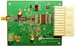
ADC14C105EB and ADC12C105EB Evaluation Boards
This User's guide applies to the ADC14C105EB and ADC12C105EB evaluation boards which are used to
evaluate the ADC14C105 and ADC12C105 A/D Converters, respectively. These ADCs belong to a family
of 12 and 14 bit converters that provide data at rates of up to 105MHz. Further reference in this manual to
the ADC14C105 is meant to also include the other listed parts unless otherwise specified.
The evaluation board is designed to be used with the WaveVision5™ Data Capture Board which is
connected to a personal computer through a USB port and running WaveVision5™ software, operating
under Microsoft Windows. The software can perform an FFT on the captured data upon command and, in
addition to a frequency domain plot, shows dynamic performance in the form of SNR, SINAD, THD SFDR
and ENOB. The latest WaveVision 5 data capture board and WaveVision 5 Software is available through
the Texas Instruments website.
Contents
Board Assembly ............................................................................................................. 2
Quick Start ................................................................................................................... 3
Functional Description ...................................................................................................... 3
3.1
Analog Input ........................................................................................................ 3
3.2
ADC Reference Circuitry .......................................................................................... 4
3.3
ADC Clock Circuit .................................................................................................. 4
3.4
Digital Data Output ................................................................................................. 4
3.5
Data Format/Duty Cycle Stabilizer ............................................................................... 4
3.6
Power Supply Connections ....................................................................................... 4
4
Installing the ADC14C105 Evaluation Board ............................................................................ 5
5
Hardware Schematic ....................................................................................................... 6
6
Bill of Materials .............................................................................................................. 8
7
Evaluation Board Layout ................................................................................................. 10
Appendix A
....................................................................................................................... 14
1
2
3
List of Figures
8
...............................................................................
Test Set Up ..................................................................................................................
Analog Input Network for FIN > 70MHz ...................................................................................
Analog Input Network for FIN < 70MHz ...................................................................................
Layer 1: Component Side ................................................................................................
Layer 2: Ground ...........................................................................................................
Layer 3: Power .............................................................................................................
Layer 4: Circuit Side ......................................................................................................
1
Bill of Materials ..............................................................................................................
1
2
3
4
5
6
7
Major Component and Jumper Locations
2
2
3
4
10
11
12
13
List of Tables
SNAU023A – July 2007 – Revised October 2013
Submit Documentation Feedback
ADC14C105EB and ADC12C105EB Evaluation Boards
Copyright © 2007–2013, Texas Instruments Incorporated
8
1
�Board Assembly
1
www.ti.com
Board Assembly
The Evaluation Board comes pre-assembled. Refer to the Bill of Materials in Section 7 for a description of
components, to Figure 1 for major component placement and to Section 5 for the Evaluation Board
schematic.
ADC14C105
JP23
J9
Input
Signal
J5
WV
Conn
TP12
VA
GND
+5V
JR1
Power
TP13
5V
TP14
VA2
J10 t Clock TP15
VD
Input
TP16
VD2
Figure 1. Major Component and Jumper Locations
Bandpass Filter
Signal Generator
PC
EVALUATION BOARD
Signal
Cond.
GND
+5V
JR1
ADC14C105
WV5
Connector
J9
Signal
Input
WV5
Connector
USB
WaveVision5 Board
J10
Clock
Input
+12V
Bandpass Filter
Power Supply
Signal Generator
Power Supply
Figure 2. Test Set Up
2
ADC14C105EB and ADC12C105EB Evaluation Boards
SNAU023A – July 2007 – Revised October 2013
Submit Documentation Feedback
Copyright © 2007–2013, Texas Instruments Incorporated
�Quick Start
www.ti.com
2
Quick Start
Refer to Figure 1 for locations of jumpers, test points and major components. Refer to Figure 2 for the test
set up. The board is configured by default to require an externally generated sampling clock. Refer to
Section 3.0 and Appendix A for more information on jumper settings. The input network of this board is
configured for input frequencies greater than 70MHz. Refer to the Analog Input section for more
information about input networks.
You must have version the WaveVision5™ data capture board and WaveVision 5 software to properly test
this board. You can download the latest version from:
http://www.ti.com/tool/wavevision5
http://www.ti.com/tool/wavevsn-brd-5.1
1. Apply power to the WaveVision5™ board and connect it to the computer using a USB cable. See the
WaveVision5™ Board Manual for operation of that board. Connect the evaluation board to the
WaveVision5™ Data Capture Board.
NOTE: power to the WaveVision5 Data Capture Board should be applied before the power to the
Evaluation Board to insure that the FPGA on the WaveVison5 Data Capture Board is not
damaged.
2. Connect a clean +5V power supply to pin 2 of Power Connector JR1. Pin 1 is ground.
3. Connect a signal from a 50-Ω source to connector J9. Be sure to use a bandpass filter before the
Evaluation Board to filter out noise and distortion from the clock signal generator.
4. Connect a signal from a 50-Ω source to connector J10. Set the amplitude to +14dBm and the
frequency to the desired sampling rate. This signal power must result in >2Vpp signal at the SMA input
to the EVM. Be sure to use a bandpass filter before the Evaluation Board to filter out noise and
distortion from the clock signal generator. See Section 3.3 for more information on signal filtering and
appropriate signal generators.
5. Adjust the input signal amplitude as needed to ensure that the signal does not over-range by
examining a histogram of the output data with the WaveVision™ software.
3
Functional Description
The Evaluation Board schematic is shown in the Hardware Schematic Section. A list of test points and
jumper settings can be found in Appendix A.
3.1
Analog Input
To obtain the best distortion results the analog input network must be optimized for the signal frequency
being applied. The Evaluation Board comes configured for input frequencies greater than 70MHz as seen
in Figure 3. The input network is intended to accept a low-noise sine wave signal of up to 2V peak-to-peak
amplitude. To accurately evaluate the dynamic performance of this converter, the input test signal will
have to be passed through a high-quality bandpass filter.
For input frequencies below 70MHz the circuit of Figure 3 may be used.
VIN
0.1uF MABA007159
0.1uF
25Ω
10pF
0.1uF
0.1uF
ADC
Input
25Ω
MABA007159
VCMO
0.1uF
Figure 3. Analog Input Network for FIN > 70MHz
For input frequencies below 70MHz the circuit of Figure 4 may be used.
SNAU023A – July 2007 – Revised October 2013
Submit Documentation Feedback
ADC14C105EB and ADC12C105EB Evaluation Boards
Copyright © 2007–2013, Texas Instruments Incorporated
3
�Functional Description
www.ti.com
VIN
20Ω
0.1 µF ADT1-1WT
18 pF
50Ω
ADC
Input
0.1 µF
0.1 µF
20Ω
VCMO
Figure 4. Analog Input Network for FIN < 70MHz
3.2
ADC Reference Circuitry
The ADC14C105 can use an internal or external 1.2V reference. This Evaluation Board is configured to
use the internal reference.
3.3
ADC Clock Circuit
Solder jumpers are used to select the path of the clock to the ADC. While not as convenient as pin-type
jumpers, these introduce less noise into the clock signal.
By default, the board requires an external signal generator to provide a low noise clock at connector J10.
The clock signal must be filtered by a bandpass filter to remove noise and distortion. On the board, the
signal is buffered by U11 (NC7WV125) and applied to the ADC’s clock input pin.
This EVM requires a 2.0-3.3 Vpp signal swing at the clock SMA which translates to +10-14.4dBm signal
power into the J10 (50-Ω) input. The chosen bandpass filter in the clock path attenuates the signal power
from the signal generator, so the generator power must set to overcome the attenuation. Different filters
have different attenuations (insertion losses). Setting +17dBm assumes a 4dB insertion loss and +13dBm
at the SMA input. The recommendation of +14dBm assumes a filter attenuation of less than 4dB.
As an option, a Pletronics SM7745 or Vectron VCC1 type device crystal clock may be placed on the
board. For this option open the pins of solder jumper JP52 and short the pins of JP45.
3.4
Digital Data Output
The digital output data is available at pins B4 (MSB) through B17 of the WaveVision™ connector J5.
3.5
Data Format/Duty Cycle Stabilizer
Output data format and the duty cycle stabilizer (DCS) are controlled by jumper JP23.
Shorting pins 1-2 of JP23 sets the output format to 2’s complement with DCS Off.
Shorting pins 3-4 of JP23 sets the output format to 2’s complement with DCS On.
Shorting pins 5-6 of JP23 sets the output format to offset binary with DCS On.
Shorting pins 7-8 of JP23 sets the output format to offset binary with DCS Off. This is the default setting.
3.6
Power Supply Connections
Power to this board is supplied through power connector JR1. The only supply needed is +5V at pin 2 plus
ground at pin 1.
Voltage and current requirements for the ADC14C105 Evaluation Board are:
• +5.0V at 500 mA
4
ADC14C105EB and ADC12C105EB Evaluation Boards
SNAU023A – July 2007 – Revised October 2013
Submit Documentation Feedback
Copyright © 2007–2013, Texas Instruments Incorporated
�Installing the ADC14C105 Evaluation Board
www.ti.com
4
Installing the ADC14C105 Evaluation Board
The evaluation board requires a single power supply as described in Power Supply Connections.
NOTE: power to the WaveVision 5 Data Capture Board should be applied before the power to the
ADC14C105 Evaluation Board to insure that the FPGA on the WaveVison5 Data Capture Board is
not damaged.
An appropriate signal source should be connected to the Signal Input SMA connector J9. When evaluating
dynamic performance, an appropriate signal generator (such as the HP8644B or the R&S SMA100A) with
50 Ω source impedance should be connected to the Analog Input connector through an appropriate
bandpass filter as even the best signal generator available can not produce a signal pure enough to
evaluate the dynamic performance of an ADC. The signal used for the clock has similar requirements and
must also be bandpass filtered.
If this board is used in conjunction with the the WaveVision5™ Data Capture Board and WaveVision5™
software, a USB cable must be connected between the Data Capture Board and the host. See the
WaveVision5™ Data Capture Board manual for details.
SNAU023A – July 2007 – Revised October 2013
Submit Documentation Feedback
ADC14C105EB and ADC12C105EB Evaluation Boards
Copyright © 2007–2013, Texas Instruments Incorporated
5
�Hardware Schematic
5
6
www.ti.com
Hardware Schematic
ADC14C105EB and ADC12C105EB Evaluation Boards
SNAU023A – July 2007 – Revised October 2013
Submit Documentation Feedback
Copyright © 2007–2013, Texas Instruments Incorporated
�Hardware Schematic
www.ti.com
SNAU023A – July 2007 – Revised October 2013
Submit Documentation Feedback
ADC14C105EB and ADC12C105EB Evaluation Boards
Copyright © 2007–2013, Texas Instruments Incorporated
7
�Bill of Materials
6
www.ti.com
Bill of Materials
Table 1. Bill of Materials
8
Item
Qty
Part Reference
Value
PCB Footprint
Manufacturered by
Part No.
Distributer
Distributer Part No.
1
1
C81
10pF
sm/c_0201_no_ss
Murata Electronics
GRM0335C1E100JD01D
Digikey
490-3142-1-ND
2
2
C117, C125
2.2nF
sm/c_0603
AVX Corporation
06031C222JAT2A
Digikey
478-3705-1-ND
3
7
C79, C84, C133, C134,
C136, C138, C140
0.01uF
sm/c_0402_no_ss
Murata Electronics
GRM155R71E103KA01D
Digikey
490-1312-1-ND
4
5
C113, C116, C142, C183,
C185, C187, C189
0.01uF
sm/c_0603
Murata Electronics
GRM188R71H103KA01D
Digikey
490-1512-1-ND
5
2
C50, C193
0.1uF
sm/c_0805
Murata Electronics
GRM21BR71E104KA01L
Digikey
490-1673-1-ND
6
8
C63, C75, C80, C106,
C109, C127, C131, C157
0.1uF
sm/c_0603
Murata Electronics
GRM188R71E104KA01D
Digikey
490-1524-1-ND
7
1
C76
0.1uF
sm/c_0201_no_ss
Murata Electronics
GRM033R61A104ME15
D
Digikey
490-5405-1-ND
8
4
C77, C78, C194, C195
0.1uF
sm/c_0402_no_ss
Murata Electronics
GRM155R71C104KA88D
Digikey
490-3261-1-ND
9
4
C112, C115, C120, C123
1uF
SM/C_1206
Murata Electronics
GRM31MF51E105ZA01L
Digikey
490-1832-1-ND
10
13
C132, C135, C137, C139,
C141, C143, C159, C181,
C182, C184, C186, C188,
C190
1uF
sm/c_0603
Murata Electronics
GRM188R61A105MA61
D
Digikey
490-1544-1-ND
11
3
C72, C73, C129
10uF
sm/ct_3216_12
Kemet
T491A106K006AT
Digikey
399-3683-2-ND
12
8
C110, C111, C114, C119,
C122, C124, C126, C156
10uF
SM/C_1206
Murata Electronics
GRM31MF51A106ZA01L
Digikey
490-1843-1-ND
13
1
C192
10uF
sm/ct_3528_12
Kemet
T491B106K010AT
Digikey
399-3705-1-ND
14
1
C74
22uF
sm/ct_3216_12
Kemet
T491A226M010AT
Digikey
399-3692-1-ND
15
1
C191
22uF
sm/ct_3528_12
Kemet
T494B226M016AT
Digikey
399-3835-1-ND
16
2
R26, R30
0.0
sm/r_0402_no_ss
Panasonic - ECG
ERJ-2GE0R00X
Digikey
P0.0JCT-ND
17
1
R154
22.1
sm/r_0603
Panasonic - ECG
ERJ-3EKF22R1V
Digikey
P22.1HCT-ND
18
2
R27, R29
24.9
sm/r_0402_no_ss
Panasonic - ECG
ERJ-2RKF24R9X
Digikey
P24.9LCT-ND
19
4
R28, R88, R116, R155
49.9
sm/r_0603
Panasonic - ECG
ERJ-3EKF49R9V
Digikey
P49.9HCT-ND
20
15
R127, R128, R129, R130,
R131, R132, R133, R134,
R135, R136, R137, R138,
R139, R140, R141
49.9
sm/r_0402_no_ss
Panasonic - ECG
ERJ-2RKF49R9X
Digikey
P49.9LCT-ND
21
7
R1, R6, R86, R89, R95,
R96, R99
1k
sm/r_0603
Panasonic - ECG
ERJ-3EKF1001V
Digikey
P1.00KHCT-ND
22
2
R3, R7
2.32k
sm/R_0603
Panasonic - ECG
ERJ-2RKF2321X
Digikey
P2.32KLCT-ND
23
1
R91
40.2k
sm/r_0603
Panasonic - ECG
ERJ-3EKF4022V
Digikey
P40.2KHCT-ND
24
3
R2, R4, R5
100K
sm/R_0603
Panasonic - ECG
ERJ-2GEJ104X
Digikey
P100KJCT-ND
25
2
RP3, RP4
RP1-220
sm/rpak_.50m/16/wg.071/l.252
CTS Resistor Products
742C163220JPTR
Digikey
742C163220JPCT-ND
26
1
L1
INDUCTOR
sm/l_1206
Murata Electronics
BLM31PG500SN1L
Digikey
490-1055-1-ND
27
1
L2
10uH
sm/l_1210
Murata Electronics
LQH32CN100K53L
Digikey
490-4059-1-ND
28
2
Z1, Z2
NFM41PC204F1H3
nfm41p
Murata Electronics
NFM41PC204F1H3L
Digikey
490-2550-1-ND
29
2
J3, J10
INPUT, EXT Clk
rf/sma/v_clr
Amphenol-RF
901-144-8RFX
Digikey
ARFX1231-ND
ADC14C105EB and ADC12C105EB Evaluation Boards
Notes
SNAU023A – July 2007 – Revised October 2013
Submit Documentation Feedback
Copyright © 2007–2013, Texas Instruments Incorporated
�Bill of Materials
www.ti.com
Table 1. Bill of Materials (continued)
Item
Qty
Part Reference
Value
PCB Footprint
Manufacturered by
Part No.
Distributer
Distributer Part No.
30
1
J9
INPUT
RF/SMA/END_LAUNCH/W.375
Emerson Network
Power Connectivity
Solutions
142-0701-801
Digikey
J502-ND
Notes
31
1
J5
FUTUREBUS_96
fbus/rs/96_ecl
Tyco Electronics
5223514-1
Provided by TI
32
1
JP21
Header2
blkcon.100/vh/tm1sqs/w.100/2
Samtec
MTSW-102-07-T-S-240
Can break apart 8-pin
MTSW-108-07-T-S-240
33
1
JP23
HEADER 4X2
blkcon.100/vh/tm2oe/w.200/8
Samtec
MTSW-104-07-T-D-240
34
1
JP52
Solder jumper
solder jumper
N/A
N/A
N/A
35
5
TP12, TP13, TP14, TP15,
TP16
VDD Test Points
tp_500X
Keystone Electronics
5002
Digikey
5002K-ND
36
4
TPG1, TPG2, TPG3, TPG4
GND Test Points
tp_500X_.125
Keystone Electronics
5011
Digikey
5011K-ND
37
1
JR1
VA / VD Power
MSTBVA2.5/2-G-5.8
Phoenix Contact
1715721
Digikey
277-1263-ND
38
1
jumper/sm
N/A
FCI
68786-302LF
Arrow
Electronics
68786-302LF
39
2
T5, T8
Transformer
sm/sot23-5/l.150/wg.150
MA/COM
MABA-007159-000000
Mouser
40
1
U5
24C02/SO8
sog.050/8/wg.244/l.200
STMicroelectronics
M24C02-RMN6TP
Digikey
497-8633-1-ND
41
1
U11
NC7WV125
SOG.50M/8/WG3.10/L2.00
Fairchild
Semiconductor
NC7WV125K8X
Mouser
512-NC7WV125K8X
42
2
U33, U34
LP3878SD-ADJ
sc-mkt-sdc08a_llp
Texas Instruments
LP3878SD-ADJ/NOPB
Digikey
LP3878SD-ADJCT-ND
43
1
U35
LP5900SD-3.3
llp6_65m_wg2p5_l2p2_ep
Texas Instruments
LP5900SD-3.3/NOPB
Digikey
LP5900SD-3.3CT-ND
44
1
U101
ADC14C105
LLP.50M/32/WG5.00
Texas Instruments
ADC14C105CISQ
Digikey
ADC14C105CISQE/NOPB
CT-ND
45
1
U108
74LVTH162244MEA
sog.025/48/wg.420/l.650
Texas Instruments
SN74LVTH162244DLR
Digikey
296-1259-1-ND
Pletronics
SM7745DV-105.0M
Online
Components
SM7745DV800MT250
Create a solder bridge to
short pads together
Short pins 7-8 of headers
JP23
Pin 1 of T5 and T8
(Xformer secondary)
faces U101
DO NOT PLACE
47
2
C67,C102
10pF *
sm/c_0402_no_ss
48
1
C103
15pF *
sm/c_0402_no_ss
49
2
C107,C108
.1uF *
sm/c_0603
50
2
R31,R32
24.9 *
sm/r_0402_no_ss
51
1
R118
49.9 *
sm/r_0603
52
1
R156
22.1 *
sm/r_0603
53
2
T3,T4
ETC1-1T *
sm/sot23-5/l.150/wg.150
54
2
T6,T7
ADT1-1WT *
adt4_6wt_xfmr
55
2
JP46, JP45
Solder jumper
46
1
Y2
Oscillator/sm4
SM/CRYSTAL/5X7
SNAU023A – July 2007 – Revised October 2013
Submit Documentation Feedback
Long Lead Item
ADC14C105EB and ADC12C105EB Evaluation Boards
Copyright © 2007–2013, Texas Instruments Incorporated
9
�Evaluation Board Layout
7
www.ti.com
Evaluation Board Layout
Figure 5. Layer 1: Component Side
10
ADC14C105EB and ADC12C105EB Evaluation Boards
SNAU023A – July 2007 – Revised October 2013
Submit Documentation Feedback
Copyright © 2007–2013, Texas Instruments Incorporated
�Evaluation Board Layout
www.ti.com
Figure 6. Layer 2: Ground
SNAU023A – July 2007 – Revised October 2013
Submit Documentation Feedback
ADC14C105EB and ADC12C105EB Evaluation Boards
Copyright © 2007–2013, Texas Instruments Incorporated
11
�Evaluation Board Layout
www.ti.com
Figure 7. Layer 3: Power
12
ADC14C105EB and ADC12C105EB Evaluation Boards
SNAU023A – July 2007 – Revised October 2013
Submit Documentation Feedback
Copyright © 2007–2013, Texas Instruments Incorporated
�Evaluation Board Layout
www.ti.com
Figure 8. Layer 4: Circuit Side
SNAU023A – July 2007 – Revised October 2013
Submit Documentation Feedback
ADC14C105EB and ADC12C105EB Evaluation Boards
Copyright © 2007–2013, Texas Instruments Incorporated
13
�www.ti.com
Appendix A
A.1
Operating with the WaveVision Hardware and Software
The ADC14C105 Evaluation Board is compatible with the WaveVision5™ Data Capture Board and
WaveVision5™ software. When connected to the WaveVision5™ Board, data capture is easily controlled
from a personal computer operating in the Windows environment. The data samples that are captured can
be observed on the PC video monitor in the time and frequency domains. The FFT analysis of the
captured data yields insight into system noise and distortion sources and estimates of ADC dynamic
performance such as SINAD, SNR, THD, SFDR and ENOB.
A.2
Summary Tables of Test Points, Connectors, and Jumper Settings
A.2.1
Connectors
JR1 Connector - Power Supply Connections
1
GND
Power Supply Ground
2
+5V
+5V Power Supply
A.2.2
Jumper Settings
Note: Default settings are in bold
JP21 : Power Down
Connect 1-2
The ADC Channel A is powered down
1-2 OPEN
The ADC is in normal operation
JP23 : Output Data Format and Duty Cycle Stabilizer
Connect 1-2
Output format of 2’s complement, DCS is OFF
Connect 3-4
Output format of 2’s complement, DCSr is ON
Connect 5-6
Output format of offset binary, DCS is ON
Connect 7-8
Output format of offset binary, DCS is OFF
A.2.3
Clock Circuit Solder Jumper settings
Solder jumpers are used to select the path of the clock to the ADC. While not as convenient as pin-type
jumpers, these introduce less noise into the clock signal.
By default the following jumpers are OPEN: JP46, JP45
By default the following jumpers are shorted: JP52
14
SNAU023A – July 2007 – Revised October 2013
Submit Documentation Feedback
Copyright © 2007–2013, Texas Instruments Incorporated
�EVALUATION BOARD/KIT/MODULE (EVM) ADDITIONAL TERMS
Texas Instruments (TI) provides the enclosed Evaluation Board/Kit/Module (EVM) under the following conditions:
The user assumes all responsibility and liability for proper and safe handling of the goods. Further, the user indemnifies TI from all claims
arising from the handling or use of the goods.
Should this evaluation board/kit not meet the specifications indicated in the User’s Guide, the board/kit may be returned within 30 days from
the date of delivery for a full refund. THE FOREGOING LIMITED WARRANTY IS THE EXCLUSIVE WARRANTY MADE BY SELLER TO
BUYER AND IS IN LIEU OF ALL OTHER WARRANTIES, EXPRESSED, IMPLIED, OR STATUTORY, INCLUDING ANY WARRANTY OF
MERCHANTABILITY OR FITNESS FOR ANY PARTICULAR PURPOSE. EXCEPT TO THE EXTENT OF THE INDEMNITY SET FORTH
ABOVE, NEITHER PARTY SHALL BE LIABLE TO THE OTHER FOR ANY INDIRECT, SPECIAL, INCIDENTAL, OR CONSEQUENTIAL
DAMAGES.
Please read the User's Guide and, specifically, the Warnings and Restrictions notice in the User's Guide prior to handling the product. This
notice contains important safety information about temperatures and voltages. For additional information on TI's environmental and/or safety
programs, please visit www.ti.com/esh or contact TI.
No license is granted under any patent right or other intellectual property right of TI covering or relating to any machine, process, or
combination in which such TI products or services might be or are used. TI currently deals with a variety of customers for products, and
therefore our arrangement with the user is not exclusive. TI assumes no liability for applications assistance, customer product design,
software performance, or infringement of patents or services described herein.
REGULATORY COMPLIANCE INFORMATION
As noted in the EVM User’s Guide and/or EVM itself, this EVM and/or accompanying hardware may or may not be subject to the Federal
Communications Commission (FCC) and Industry Canada (IC) rules.
For EVMs not subject to the above rules, this evaluation board/kit/module is intended for use for ENGINEERING DEVELOPMENT,
DEMONSTRATION OR EVALUATION PURPOSES ONLY and is not considered by TI to be a finished end product fit for general consumer
use. It generates, uses, and can radiate radio frequency energy and has not been tested for compliance with the limits of computing
devices pursuant to part 15 of FCC or ICES-003 rules, which are designed to provide reasonable protection against radio frequency
interference. Operation of the equipment may cause interference with radio communications, in which case the user at his own expense will
be required to take whatever measures may be required to correct this interference.
General Statement for EVMs including a radio
User Power/Frequency Use Obligations: This radio is intended for development/professional use only in legally allocated frequency and
power limits. Any use of radio frequencies and/or power availability of this EVM and its development application(s) must comply with local
laws governing radio spectrum allocation and power limits for this evaluation module. It is the user’s sole responsibility to only operate this
radio in legally acceptable frequency space and within legally mandated power limitations. Any exceptions to this are strictly prohibited and
unauthorized by Texas Instruments unless user has obtained appropriate experimental/development licenses from local regulatory
authorities, which is responsibility of user including its acceptable authorization.
For EVMs annotated as FCC – FEDERAL COMMUNICATIONS COMMISSION Part 15 Compliant
Caution
This device complies with part 15 of the FCC Rules. Operation is subject to the following two conditions: (1) This device may not cause
harmful interference, and (2) this device must accept any interference received, including interference that may cause undesired operation.
Changes or modifications not expressly approved by the party responsible for compliance could void the user's authority to operate the
equipment.
FCC Interference Statement for Class A EVM devices
This equipment has been tested and found to comply with the limits for a Class A digital device, pursuant to part 15 of the FCC Rules.
These limits are designed to provide reasonable protection against harmful interference when the equipment is operated in a commercial
environment. This equipment generates, uses, and can radiate radio frequency energy and, if not installed and used in accordance with the
instruction manual, may cause harmful interference to radio communications. Operation of this equipment in a residential area is likely to
cause harmful interference in which case the user will be required to correct the interference at his own expense.
�FCC Interference Statement for Class B EVM devices
This equipment has been tested and found to comply with the limits for a Class B digital device, pursuant to part 15 of the FCC Rules.
These limits are designed to provide reasonable protection against harmful interference in a residential installation. This equipment
generates, uses and can radiate radio frequency energy and, if not installed and used in accordance with the instructions, may cause
harmful interference to radio communications. However, there is no guarantee that interference will not occur in a particular installation. If
this equipment does cause harmful interference to radio or television reception, which can be determined by turning the equipment off and
on, the user is encouraged to try to correct the interference by one or more of the following measures:
• Reorient or relocate the receiving antenna.
• Increase the separation between the equipment and receiver.
• Connect the equipment into an outlet on a circuit different from that to which the receiver is connected.
• Consult the dealer or an experienced radio/TV technician for help.
For EVMs annotated as IC – INDUSTRY CANADA Compliant
This Class A or B digital apparatus complies with Canadian ICES-003.
Changes or modifications not expressly approved by the party responsible for compliance could void the user’s authority to operate the
equipment.
Concerning EVMs including radio transmitters
This device complies with Industry Canada licence-exempt RSS standard(s). Operation is subject to the following two conditions: (1) this
device may not cause interference, and (2) this device must accept any interference, including interference that may cause undesired
operation of the device.
Concerning EVMs including detachable antennas
Under Industry Canada regulations, this radio transmitter may only operate using an antenna of a type and maximum (or lesser) gain
approved for the transmitter by Industry Canada. To reduce potential radio interference to other users, the antenna type and its gain should
be so chosen that the equivalent isotropically radiated power (e.i.r.p.) is not more than that necessary for successful communication.
This radio transmitter has been approved by Industry Canada to operate with the antenna types listed in the user guide with the maximum
permissible gain and required antenna impedance for each antenna type indicated. Antenna types not included in this list, having a gain
greater than the maximum gain indicated for that type, are strictly prohibited for use with this device.
Cet appareil numérique de la classe A ou B est conforme à la norme NMB-003 du Canada.
Les changements ou les modifications pas expressément approuvés par la partie responsable de la conformité ont pu vider l’autorité de
l'utilisateur pour actionner l'équipement.
Concernant les EVMs avec appareils radio
Le présent appareil est conforme aux CNR d'Industrie Canada applicables aux appareils radio exempts de licence. L'exploitation est
autorisée aux deux conditions suivantes : (1) l'appareil ne doit pas produire de brouillage, et (2) l'utilisateur de l'appareil doit accepter tout
brouillage radioélectrique subi, même si le brouillage est susceptible d'en compromettre le fonctionnement.
Concernant les EVMs avec antennes détachables
Conformément à la réglementation d'Industrie Canada, le présent émetteur radio peut fonctionner avec une antenne d'un type et d'un gain
maximal (ou inférieur) approuvé pour l'émetteur par Industrie Canada. Dans le but de réduire les risques de brouillage radioélectrique à
l'intention des autres utilisateurs, il faut choisir le type d'antenne et son gain de sorte que la puissance isotrope rayonnée équivalente
(p.i.r.e.) ne dépasse pas l'intensité nécessaire à l'établissement d'une communication satisfaisante.
Le présent émetteur radio a été approuvé par Industrie Canada pour fonctionner avec les types d'antenne énumérés dans le manuel
d’usage et ayant un gain admissible maximal et l'impédance requise pour chaque type d'antenne. Les types d'antenne non inclus dans
cette liste, ou dont le gain est supérieur au gain maximal indiqué, sont strictement interdits pour l'exploitation de l'émetteur.
SPACER
SPACER
SPACER
SPACER
SPACER
SPACER
SPACER
SPACER
�【Important Notice for Users of EVMs for RF Products in Japan】
】
This development kit is NOT certified as Confirming to Technical Regulations of Radio Law of Japan
If you use this product in Japan, you are required by Radio Law of Japan to follow the instructions below with respect to this product:
1.
2.
3.
Use this product in a shielded room or any other test facility as defined in the notification #173 issued by Ministry of Internal Affairs and
Communications on March 28, 2006, based on Sub-section 1.1 of Article 6 of the Ministry’s Rule for Enforcement of Radio Law of
Japan,
Use this product only after you obtained the license of Test Radio Station as provided in Radio Law of Japan with respect to this
product, or
Use of this product only after you obtained the Technical Regulations Conformity Certification as provided in Radio Law of Japan with
respect to this product. Also, please do not transfer this product, unless you give the same notice above to the transferee. Please note
that if you could not follow the instructions above, you will be subject to penalties of Radio Law of Japan.
Texas Instruments Japan Limited
(address) 24-1, Nishi-Shinjuku 6 chome, Shinjuku-ku, Tokyo, Japan
http://www.tij.co.jp
【無線電波を送信する製品の開発キットをお使いになる際の注意事項】
本開発キットは技術基準適合証明を受けておりません。
本製品のご使用に際しては、電波法遵守のため、以下のいずれかの措置を取っていただく必要がありますのでご注意ください。
1.
2.
3.
電波法施行規則第6条第1項第1号に基づく平成18年3月28日総務省告示第173号で定められた電波暗室等の試験設備でご使用いただく。
実験局の免許を取得後ご使用いただく。
技術基準適合証明を取得後ご使用いただく。
なお、本製品は、上記の「ご使用にあたっての注意」を譲渡先、移転先に通知しない限り、譲渡、移転できないものとします。
上記を遵守頂けない場合は、電波法の罰則が適用される可能性があることをご留意ください。
日本テキサス・インスツルメンツ株式会社
東京都新宿区西新宿6丁目24番1号
西新宿三井ビル
http://www.tij.co.jp
SPACER
SPACER
SPACER
SPACER
SPACER
SPACER
SPACER
SPACER
SPACER
SPACER
SPACER
SPACER
SPACER
SPACER
SPACER
SPACER
SPACER
�EVALUATION BOARD/KIT/MODULE (EVM)
WARNINGS, RESTRICTIONS AND DISCLAIMERS
For Feasibility Evaluation Only, in Laboratory/Development Environments. Unless otherwise indicated, this EVM is not a finished
electrical equipment and not intended for consumer use. It is intended solely for use for preliminary feasibility evaluation in
laboratory/development environments by technically qualified electronics experts who are familiar with the dangers and application risks
associated with handling electrical mechanical components, systems and subsystems. It should not be used as all or part of a finished end
product.
Your Sole Responsibility and Risk. You acknowledge, represent and agree that:
1.
2.
3.
4.
You have unique knowledge concerning Federal, State and local regulatory requirements (including but not limited to Food and Drug
Administration regulations, if applicable) which relate to your products and which relate to your use (and/or that of your employees,
affiliates, contractors or designees) of the EVM for evaluation, testing and other purposes.
You have full and exclusive responsibility to assure the safety and compliance of your products with all such laws and other applicable
regulatory requirements, and also to assure the safety of any activities to be conducted by you and/or your employees, affiliates,
contractors or designees, using the EVM. Further, you are responsible to assure that any interfaces (electronic and/or mechanical)
between the EVM and any human body are designed with suitable isolation and means to safely limit accessible leakage currents to
minimize the risk of electrical shock hazard.
Since the EVM is not a completed product, it may not meet all applicable regulatory and safety compliance standards (such as UL,
CSA, VDE, CE, RoHS and WEEE) which may normally be associated with similar items. You assume full responsibility to determine
and/or assure compliance with any such standards and related certifications as may be applicable. You will employ reasonable
safeguards to ensure that your use of the EVM will not result in any property damage, injury or death, even if the EVM should fail to
perform as described or expected.
You will take care of proper disposal and recycling of the EVM’s electronic components and packing materials.
Certain Instructions. It is important to operate this EVM within TI’s recommended specifications and environmental considerations per the
user guidelines. Exceeding the specified EVM ratings (including but not limited to input and output voltage, current, power, and
environmental ranges) may cause property damage, personal injury or death. If there are questions concerning these ratings please contact
a TI field representative prior to connecting interface electronics including input power and intended loads. Any loads applied outside of the
specified output range may result in unintended and/or inaccurate operation and/or possible permanent damage to the EVM and/or
interface electronics. Please consult the EVM User's Guide prior to connecting any load to the EVM output. If there is uncertainty as to the
load specification, please contact a TI field representative. During normal operation, some circuit components may have case temperatures
greater than 60°C as long as the input and output are maintained at a normal ambient operating temperature. These components include
but are not limited to linear regulators, switching transistors, pass transistors, and current sense resistors which can be identified using the
EVM schematic located in the EVM User's Guide. When placing measurement probes near these devices during normal operation, please
be aware that these devices may be very warm to the touch. As with all electronic evaluation tools, only qualified personnel knowledgeable
in electronic measurement and diagnostics normally found in development environments should use these EVMs.
Agreement to Defend, Indemnify and Hold Harmless. You agree to defend, indemnify and hold TI, its licensors and their representatives
harmless from and against any and all claims, damages, losses, expenses, costs and liabilities (collectively, "Claims") arising out of or in
connection with any use of the EVM that is not in accordance with the terms of the agreement. This obligation shall apply whether Claims
arise under law of tort or contract or any other legal theory, and even if the EVM fails to perform as described or expected.
Safety-Critical or Life-Critical Applications. If you intend to evaluate the components for possible use in safety critical applications (such
as life support) where a failure of the TI product would reasonably be expected to cause severe personal injury or death, such as devices
which are classified as FDA Class III or similar classification, then you must specifically notify TI of such intent and enter into a separate
Assurance and Indemnity Agreement.
Mailing Address: Texas Instruments, Post Office Box 655303, Dallas, Texas 75265
Copyright © 2013, Texas Instruments Incorporated
�IMPORTANT NOTICE
Texas Instruments Incorporated and its subsidiaries (TI) reserve the right to make corrections, enhancements, improvements and other
changes to its semiconductor products and services per JESD46, latest issue, and to discontinue any product or service per JESD48, latest
issue. Buyers should obtain the latest relevant information before placing orders and should verify that such information is current and
complete. All semiconductor products (also referred to herein as “components”) are sold subject to TI’s terms and conditions of sale
supplied at the time of order acknowledgment.
TI warrants performance of its components to the specifications applicable at the time of sale, in accordance with the warranty in TI’s terms
and conditions of sale of semiconductor products. Testing and other quality control techniques are used to the extent TI deems necessary
to support this warranty. Except where mandated by applicable law, testing of all parameters of each component is not necessarily
performed.
TI assumes no liability for applications assistance or the design of Buyers’ products. Buyers are responsible for their products and
applications using TI components. To minimize the risks associated with Buyers’ products and applications, Buyers should provide
adequate design and operating safeguards.
TI does not warrant or represent that any license, either express or implied, is granted under any patent right, copyright, mask work right, or
other intellectual property right relating to any combination, machine, or process in which TI components or services are used. Information
published by TI regarding third-party products or services does not constitute a license to use such products or services or a warranty or
endorsement thereof. Use of such information may require a license from a third party under the patents or other intellectual property of the
third party, or a license from TI under the patents or other intellectual property of TI.
Reproduction of significant portions of TI information in TI data books or data sheets is permissible only if reproduction is without alteration
and is accompanied by all associated warranties, conditions, limitations, and notices. TI is not responsible or liable for such altered
documentation. Information of third parties may be subject to additional restrictions.
Resale of TI components or services with statements different from or beyond the parameters stated by TI for that component or service
voids all express and any implied warranties for the associated TI component or service and is an unfair and deceptive business practice.
TI is not responsible or liable for any such statements.
Buyer acknowledges and agrees that it is solely responsible for compliance with all legal, regulatory and safety-related requirements
concerning its products, and any use of TI components in its applications, notwithstanding any applications-related information or support
that may be provided by TI. Buyer represents and agrees that it has all the necessary expertise to create and implement safeguards which
anticipate dangerous consequences of failures, monitor failures and their consequences, lessen the likelihood of failures that might cause
harm and take appropriate remedial actions. Buyer will fully indemnify TI and its representatives against any damages arising out of the use
of any TI components in safety-critical applications.
In some cases, TI components may be promoted specifically to facilitate safety-related applications. With such components, TI’s goal is to
help enable customers to design and create their own end-product solutions that meet applicable functional safety standards and
requirements. Nonetheless, such components are subject to these terms.
No TI components are authorized for use in FDA Class III (or similar life-critical medical equipment) unless authorized officers of the parties
have executed a special agreement specifically governing such use.
Only those TI components which TI has specifically designated as military grade or “enhanced plastic” are designed and intended for use in
military/aerospace applications or environments. Buyer acknowledges and agrees that any military or aerospace use of TI components
which have not been so designated is solely at the Buyer's risk, and that Buyer is solely responsible for compliance with all legal and
regulatory requirements in connection with such use.
TI has specifically designated certain components as meeting ISO/TS16949 requirements, mainly for automotive use. In any case of use of
non-designated products, TI will not be responsible for any failure to meet ISO/TS16949.
Products
Applications
Audio
www.ti.com/audio
Automotive and Transportation
www.ti.com/automotive
Amplifiers
amplifier.ti.com
Communications and Telecom
www.ti.com/communications
Data Converters
dataconverter.ti.com
Computers and Peripherals
www.ti.com/computers
DLP® Products
www.dlp.com
Consumer Electronics
www.ti.com/consumer-apps
DSP
dsp.ti.com
Energy and Lighting
www.ti.com/energy
Clocks and Timers
www.ti.com/clocks
Industrial
www.ti.com/industrial
Interface
interface.ti.com
Medical
www.ti.com/medical
Logic
logic.ti.com
Security
www.ti.com/security
Power Mgmt
power.ti.com
Space, Avionics and Defense
www.ti.com/space-avionics-defense
Microcontrollers
microcontroller.ti.com
Video and Imaging
www.ti.com/video
RFID
www.ti-rfid.com
OMAP Applications Processors
www.ti.com/omap
TI E2E Community
e2e.ti.com
Wireless Connectivity
www.ti.com/wirelessconnectivity
Mailing Address: Texas Instruments, Post Office Box 655303, Dallas, Texas 75265
Copyright © 2013, Texas Instruments Incorporated
�


 工商网监
湘ICP备2023018690号
工商网监
湘ICP备2023018690号
