®
ADC76
16-Bit
ANALOG-TO-DIGITAL CONVERTER
FEATURES
DESCRIPTION
● 16-BIT RESOLUTION
● LINEARITY ERROR: ±0.003% max (KG, BG)
● NO MISSING CODES GUARANTEED
FROM –25°C TO +85°C
● 17µs CONVERSION TIME (16-Bit)
● SERIAL AND PARALLEL OUTPUTS
The ADC76 is a high quality, 16-bit successive approximation analog-to-digital converter. The ADC76
uses state-of-the-art laser-trimmed IC thin-film resistors and is packaged in a hermetic 32-pin dual-in-line
package. The converter is complete with internal reference, short cycling capabilities, serial output, and
thin-film scaling resistors, which allow selection of
analog input ranges of ±2.5V, ±5V, ±10V, 0 to +5V,
0 to +10V and 0 to +20V.
It is specified for operation over two temperature
ranges: 0°C to +70°C (J, K) and –25°C to +85°C (A, B).
Data is available in parallel and serial form with
corresponding clock and status output. All digital
inputs and outputs are TTL-compatible.
Power supply voltages are ±15VDC and +5VDC.
Parallel
Digital
Output
16-Bit D/A
Converter
Reference
16-Bit
Successive Approx.
Register (SAR)
Short Cycle
Convert Command
Range
}Input
Select
–
Comparator In
+
Clock Rate Control
Clock Out
Status
Serial Out
Clock
International Airport Industrial Park • Mailing Address: PO Box 11400 • Tucson, AZ 85734 • Street Address: 6730 S. Tucson Blvd. • Tucson, AZ 85706
Tel: (520) 746-1111 • Twx: 910-952-1111 • Cable: BBRCORP • Telex: 066-6491 • FAX: (520) 889-1510 • Immediate Product Info: (800) 548-6132
©
1990 Burr-Brown Corporation
PDS-1063A
Printed in U.S.A. December, 1993
�SPECIFICATIONS
ELECTRICAL
At +25°C, and rated power supplies, unless otherwise noted.
ADC76J, K
MODEL
MIN
ADC76A, B
TYP
MAX
RESOLUTION
MIN
TYP
16
ANALOG INPUTS
Voltage Ranges: Bipolar
Unipolar
Impedance (Direct Input)
0 to +5V, ±2.5V
0 to +10V, ±5.0V
0 to +20V, ±10V
DIGITAL INPUTS(1)
Convert Command
Logic Loading
MAX
UNITS
*
Bits
±2.5, ±5, ±10
0 to +5, 0 to +10
0 to +20
*
*
*
V
V
2.5
5
10
*
*
*
kΩ
kΩ
kΩ
Positive pulse 50ns wide (min) trailing edge (“1” to “0” initiates conversion)
1
*
TTL Load
*
*
*
*
*
%
% of FSR(3)
% of FSR
% of FSR
% of FSR
LSB
% of FSR
% of FSR
TRANSFER CHARACTERISTICS
ACCURACY
Gain Error(2)
Offset Error: Unipolar(2)
Bipolar(2)
Linearity Error: K, B
J, A
Inherent Quantization Error
Differential Linearity Error
Noise (3σ, p-p)
±1/2
±0.003
±0.001
POWER SUPPLY SENSITIVITY
±15VDC
+5VDC
0.003
0.001
±0.1
±0.05
±0.1
±0.2
±0.1
±0.2
±0.003
±0.006
OUTPUT DIGITAL DATA
(All codes complementary)
Parallel
Output Codes(5): Unipolar
Bipolar
Output Drive
Serial Data Code (NRZ)
Output Drive
Status
Status Output Drive
Internal Clock: Clock Output Drive
Frequency(7)
POWER SUPPLY REOUIREMENTS
Power Consumption
Rated Voltage: Analog
Digital
Supply Drain: +15VDC
–15VDC
+5VDC
15
16
17
TEMPERATURE RANGE
Specification
Storage
% of FSR/%VS
% of FSR/%VS
*
*
*
*
±15
±4
±10
±3
±2
±2
0
0
+70
+70
µs
µs
µs
Min
*
*
–25
–25
CSB
COB, CTC(6)
*
*
*
*
ppm/°C
ppm of FSR/°C
ppm of FSR/°C
ppm of FSR/°C
+85
+85
°C
°C
*
TTL Loads
*
TTL Loads
*
*
*
TTL Loads
TTL Loads
kHz
*
*
*
*
*
W
VDC
VDC
mA
mA
mA
+85
*
°C
°C
*
*
2
CSB, COB
*
2
Logic “1” during conversion
*
2
2
1400
933
±11.4
+4.75
*
*
*
5
DRIFT
Gain
Offset: Unipolar
Bipolar
Linearity
No Missing Codes Temp Range
J, A (13-bit)
K, B (14-bit)
*
*
*
±0.003
CONVERSION TIME(4)
14 Bits
15 Bits
16 Bits
WARM-UP TIME
*
*
*
0.655
±15
+5
+10
–28
+17
0
–55
*
±16
+5.25
+15
–35
+20
*
*
+70
+125
–25
*
*
*
*
*
*
*
*Specification same as ADC76J, K.
NOTES: (1) CMOS/TTL compatible, i.e., Logic “0” = 0.8V, max, Logic “1” = 2.0V, min for inputs. For digital outputs Logic “0” = 0.4V, max, Logic “1’ = 2.4V, min.
(2) Adjustable to zero. See “Optional External Gain and Offset Adjustment” section. (3) FSR means Full Scale Range. For example, unit connected for ±10V range
has 20V FSR. (4) Conversion time may be shortened with “Short Cycle” set for lower resolution and with use of Clock Rate Control. See “Optional Conversion Time
Adjustment” section. The Clock Rate Control (pin 23) should be connected to Digital Common for specified conversion time. Short Cycle (pin 32) should be left open
for 16-bit resolution or connected to the n + 1 digital output for n-bit resolution. For example, connect Short Cycle to Bit 15 (pin 15) for 14-bit resolution. For resolutions
less than 16 bits, pin 32 should also be tied to +5V through a 2kΩ resistor. (5) See Table I. CSB = Complementary Straight Binary, COB = Complementary Offset
Binary, CTC = Complementary Two’s Complement. (6) CTC coding obtained by inverting MSB (pin 1). (7) Adjustable with Clock Rate Control from approximately
933kHz to 1.4MHz.
®
ADC76
2
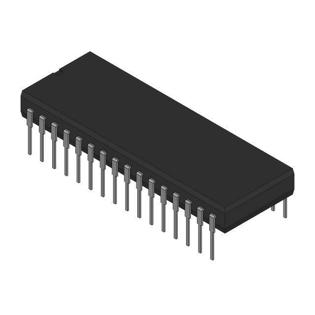
�PIN CONFIGURATION
Top View
DIP
32 Short Cycle
MSB Bit 1 1
Bit 2 2
31 Convert Command
Bit 3 3
30 +5V Supply
16-Bit D/A Converter
Bit 4 4
16-Bit SAR
Bit 5 5
Bit 6 6
Bit 7 7
Bit 8 8
Bit 9 9
29 Gain Adjust
Reference
28 +15V Supply
27 Comparator In
6.3kΩ
26 Bipolar Offset
5kΩ
5kΩ
25 10V
24 20V
23 Clock Rate Control
Bit 10 10
Bit 11 11
Bit 12 12
(LSB for 13 Bits) Bit 13 13
–
22 Analog Common(1)
+
21 –15V Supply
20 Clock Out
Comparator
(LSB for 14 Bits) Bit 14 14
19 Digital Common
Bit 15 15
18 Status
Clock
Bit 16 16
17 Serial Out
NOTE: (1) Metal lid is connected
to pin 22 (Analog Common).
ABSOLUTE MAXIMUM SPECIFICATIONS
PACKAGE INFORMATION
+VCC to Common .................................................................. 0V to +16.5V
–VCC to Common .................................................................. 0V to –16.5V
+VDD to Common ....................................................................... 0V to +7V
Analog Common to Digital Common ............................................... ±0.5V
Logic Inputs to Common ........................................................... 0V to VDD
Maximum Power Dissipation ....................................................... 1000mW
Lead Temperature (soldering, 10s) ................................................. 300°C
MODEL
ADC76JG
ADC76KG
ADC76AG
ADC76BG
PACKAGE DRAWING
NUMBER(1)
PACKAGE
32-Pin
32-Pin
32-Pin
32-Pin
Hermetic
Hermetic
Hermetic
Hermetic
DIP
DIP
DIP
DIP
172-5
172-5
172-5
172-5
NOTE: (1) For detailed drawing and dimension table, please see end of data
sheet, or Appendix D of Burr-Brown IC Data Book.
ORDERING INFORMATION
MODEL
ADC76AG
ADC76BG
ADC76JG
ADC76KG
LINEARITY ERROR
max (% of FSR)
TEMPERATURE RANGE
±0.006
±0.003
±0.006
±0.003
–25°C to +85°C
–25°C to +85°C
0°C to +70°C
0°C to +70°C
1-24
25-99
100-249
The information provided herein is believed to be reliable; however, BURR-BROWN assumes no responsibility for inaccuracies or omissions. BURR-BROWN assumes
no responsibility for the use of this information, and all use of such information shall be entirely at the user’s own risk. Prices and specifications are subject to change
without notice. No patent rights or licenses to any of the circuits described herein are implied or granted to any third party. BURR-BROWN does not authorize or warrant
any BURR-BROWN product for use in life support devices and/or systems.
®
3
ADC76
�Convert Command
Maximum Throughput Time(2)
Conversion Time
(1)
Internal Clock
Status (EOC)
“0”
MBS
Bit 2
“1”
Bit 3
“1”
“0”
Bit 4
“0”
Bit 5
Bit 6
“1”
Bit 7
“1”
Bit 8
“1”
“0”
Bit 9
Bit 10
“1”
Bit 11
“1”
“0”
Bit 12
Bit 13
“1”
“0”
Bit 14
“0”
Bit 15
Bit 16
Serial Data Out
MSB
1
2
3
4
5
6
7
8
9
10
11
12
13
14
15
“1”
16
“0”
“1”
“1”
“0”
“0”
“1”
“1”
“1”
“0”
“1”
“1”
“0”
“1”
“0”
“0”
“1”
NOTES: (1) The convert command must be at least 50ns wide and must remain low during a conversion. The conversion is
initiated by the “trailing edge” of the convert command. (2) 17µs for 16 bits.
FIGURE 1. ADC76 Timing Diagram.
Serial
Out
40-125ns
40-125ns
Bit 16
Valid
Bit 16
Clock
Out
40-125ns
Status
FIGURE 2. Timing Relationship of Serial Data to Clock.
BINARY
(BIN) OUTPUT
FIGURE 3. Timing Relationship of Valid Data to Status.
INPUT VOLTAGE RANGE AND LSB VALUES
Analog Input
Voltage Range
±10V
±5V
±2.5V
0 to +10V
0 to +5V
0 to +20V
COB(1)
or CTC(2)
COB(1)
or CTC(2)
COB(1)
or CTC(2)
CSB(3)
CSB(3)
CSB(3)
FSR
2n
n = 12
n = 13
n = 14
20V
2n
4.88mV
2.44mV
1.22mV
10V
2n
2.44mV
1.22mV
610µV
5V
2n
1.22mV
610µV
305µV
10V
2n
2.44mV
1.22mV
610µV
5V
2n
1.22mV
610µV
305µV
20V
2n
4.88mV
2.44mV
1.22mV
+Full Scale
Mid Scale
–Full Scale
+10V–3/2LSB
0
–10V +1/2LSB
+5V–3/2LSB
0
–5V +1/2LSB
+2.5V–3/2LSB
0
–2.5V +1/2LSB
+10V–3/2LSB
+5V
0 +1/2LSB
+5V–3/2LSB
+2.5V
0 +1/2LSB
+20V–3/2LSB
+10V
0 +1/2LSB
Defined As:
Code
Designation
One Least
Significant
Bit (LSB)
Transition Values
MSB LSB
000 ... 000(4)
011 ... 111
111 ... 110
NOTES: (1) COB = Complementary Offset Binary. (2) Complementary Two’s Complement—obtained by inverting the most significant bit MSB (pin 1).
(3) CSB = Complementary Straight Binary. (4) Voltages given are the nominal value for transition to the code specified.
TABLE I. Input Voltages, Transition Values, LSB Values, and Code Definitions.
®
ADC76
4
�TYPICAL PERFORMANCE CURVES
TA = +25°C, VCC = ±15V unless otherwise noted.
POWER SUPPLY REJECTION vs
SUPPLY RIPPLE FREQUENCY
% of FSR Error per % of Change In VSUPPLY
GAIN DRIFT ERROR (% OF FSR)
vs TEMPERATURE
Gain Drift Error (% of FSR)
+0.08
+0.04
0
–0.04
+85
+25
Temperature (°C)
THEORY OF OPERATION
The accuracy of a successive approximation A/D converter
is described by the transfer function shown in Figure 1. All
successive approximation A/ D converters have an inherent
quantization error of ±1/ 2LSB. The remaining errors in the
A/ D converter are combinations of analog errors due to the
linear circuitry, matching and tracking properties of the
ladder and scaling networks, power supply rejection, and
reference errors. In summary, these errors consist of initial
errors including Gain, Offset, Linearity, Differential Linearity, and Power Supply Sensitivity. Initial Gain and Offset
errors may be adjusted to zero. Gain drift over temperature
rotates the line (Figure l) about the zero or minus full scale
point (all bits Off) and Offset drift shifts the line left or right
over the operating temperature range. Linearity error is
unadjustable and is the most meaningful indicator of A/ D
converter accuracy. Linearity error is the deviation of an
actual bit transition from the ideal transition value at any
level over the range of the A/ D converter. A differential
linearity error of ±1/ 2LSB means that the width of each bit
step over the range of the A/ D converter is 1LSB, ±1/ 2LSB.
Digital Output (COB Code)*
1000 ... 0001
+1/2LSB
All Bits Off
Analog Input
–FSR/2
0.001
1
10
100
1k
Frequency (Hz)
10k
100k
Table I shows the LSB, transition values, and code definitions for each possible analog input signal range for 12-, 13and 14-bit resolutions. Figure 5 shows the connections for
14-bit resolution, parallel data output, with ±10V input.
1111 ... 1110
1111 ... 1111
+5VDC
0.002
Parallel Data
Two binary codes are available on the ADC76 parallel
output: they are complementary (logic “0” is true) straight
binary (CSB) for unipolar input signal ranges, and complementary offset binary (COB) for bipolar input signal ranges.
Complementary two’s complement (CTC) may be obtained
by inverting the MSB (pin 1).
–1/2LSB
Offset
Error
+15VDC
0.006
0.004
DIGITAL CODES
0111 ... 1111
1000 ... 0000
0.01
The timing diagram in Figure 2 assumes an analog input
such that the positive true digital word 1001 1000 1001 0110
exists. The output will be complementary as shown in Figure
2 (0110 0111 0110 1001 is the digital output). Figures 3 and
4 are timing diagrams showing the relationship of serial data
to clock, and valid data to status.
0011 ... 1100
0011 ... 1110
0.02
TIMING CONSIDERATIONS
Gain
Error
0000 ... 0001
–15VDC
0.04
temperature range when short cycled for 14-bit operation
All Bit On
0000 ... 0000
0.06
NOTE: Pages
4&5 were
switched for
abridge version
for '96 data book.
The ADC76 is also monotonic, assuring that the output
sure
toor remains
switch
digitalBe
code either
increases
the same for increasing analog input signals. Burr-Brown also guarantees that
back for full PDS.
this converter will have no missing codes over a specified
–0.08
–0.12
–25
0.1
Serial Data
eIN On
Two straight binary (complementary) codes are available on
the serial output line: CSB and COB. The serial data is
available only during conversion and appears with MSB
occurring first. The serial data is synchronous with the
internal clock as shown in the timing diagrams of Figures 2
and 3. The LSB and transition values shown in Table I also
apply to the serial data output except for the CTC code.
+FSR/2–1LSB
eIN Off
*See Table I for Digital Code Definitions.
FIGURE 1. Input vs Output for an Ideal Bipolar A/ D
Converter.
®
5
ADC76
�+5
2kΩ
MSB
32
1
2
Dotted Lines
Are External
Connections
3
Logic Output 14 Bits
4
NC
30
28
6
27
7
26
8
Convert Command From
Control Logic
+5VDC
270k Ω
29
5
ADC76
0.01µF*
31
+
1.8M Ω
Bipolar
Offset
Gain
Adjust
10k Ω to
100k Ω
+15VDC
1µF
Offset
Adjust
25
9
24
10
23
11
22
12
21
13
20
14
19
15
18
16
17 Serial Out
+
10k Ω to
100k Ω
1µF
Analog Input
±10V
Analog
Common
1µF
+
1µF
–15VDC
Digital
Common
Status Output to
Control Logic
*Capacitor should be connected even if external gain adjust is not used.
FIGURE 5. ADC76 Connections for: ±10V Analog Input, 14-Bit Resolution (Short-Cycled), Parallel Data Output.
DISCUSSION
OF SPECIFICATIONS
DIFFERENTIAL LINEARITY ERROR
Differential linearity describes the step size between transition values. A differential linearity error of ±0.003% of FSR
indicates that the size of any step may not vary from the ideal
step size by more than 0.003% of Full Scale Range.
The ADC76 is specified to meet critical performance criteria
for a wide variety of applications. The most critical specifications for an A/ D converter are linearity, drift, gain and
offset errors, and conversion speed effects on accuracy. This
ADC is factory-trimmed and tested for all critical key
specifications.
ACCURACY VERSUS SPEED
In successive approximation A/ D converters, the conversion speed affects linearity and differential linearity errors.
Conversion speed and its effect on linearity and differential
linearity errors for the ADC76 are shown in Figure 6.
GAIN AND OFFSET ERROR
Initial Gain and Offset errors are factory-trimmed to typically ±0.1% of FSR (±0.05% for unipolar offset) at 25°C.
These errors may be trimmed to zero by connecting external
trim potentiometers as shown in Figures 10 and 11.
POWER SUPPLY SENSITIVITY
Changes in the DC power supply voltages will affect accuracy. The ADC76 power supply sensitivity is specified at
±0.003% of FSR/%VS for the ±15V supplies and ±0.0015%
of FSR/%VS for the +5V supply. Normally, regulated power
supplies with 1% or less ripple are recommended for use
with this ADC. See Layout Precautions, Power Supply
Decoupling, and Figure 7.
Linearity and Differential Linearity
Error (% of FSR)
0.01
LINEARITY ERROR
Short Cycled to 14 Bits
0.006
1/2LSB 13 Bit
0.003
0.001
10
Linearity error is not adjustable and is the most meaningful
indicator of A/ D converter accuracy. Linearity is the deviation of an actual bit transition from the ideal transition value
at any level over the range of the A/ D converter.
11
12
13
14
Conversion Time (µs)
FIGURE 6. Linearity Versus Conversion Time.
®
ADC76
Short Cycled to 13 Bits
1/2LSB 14 Bit
6
15
�LAYOUT AND
OPERATING INSTRUCTIONS
Direct
Input
22
24
R2
LAYOUT PRECAUTIONS
5kΩ
Analog and digital common are not connected internally in
the ADC76, but should be connected together as close to the
unit as possible, preferably to a large plane under the ADC.
If these grounds must be run separately, use a wide conductor pattern and a 0.01µF to 0.1µF nonpolarized bypass
capacitor between analog and digital commons at the unit.
Low impedance analog and digital common returns are
essential for low noise performance. Coupling between
analog inputs and digital lines should be minimized by
careful layout. The comparator input (pin 27) is extremely
sensitive to noise. Any connection to this point should be as
short as possible and shielded by Analog Common or
±15VDC supply patterns.
Comp
In
R1
5kΩ
27
26 6.3kΩ
Bipolar
Offset
From D/A
Converter
VREF
Comparator
to Logic
FIGURE 8. ADC76 Input Scaling Circuit.
OUTPUT DRIVE
Normally all ADC76 logic outputs will drive two standard
TTL loads; however, if long digital lines must be driven,
external logic buffers are recommended.
INPUT IMPEDANCE
The input signal to the ADC76 should be low impedance,
such as the output of an op amp, to avoid any errors due to
the relatively low input impedance of the ADC76.
POWER SUPPLY DECOUPLING
The power supplies should be bypassed with tantalum or
electrolytic capacitors as shown in Figure 7 to obtain noise
free operation. These capacitors should be located close to
the ADC.
21
25
If this impedance is not low, a buffer amplifier should be
added between the input signal and the direct input to the
ADC76 as shown in Figure 9.
–15VDC
30
+5VDC
1µF
+
+
22
Analog
Common
Analog
Input Signal
1µF
19
1µF
Digital
Common
10MΩ
+
Connect to
Pin 24 or Pin 25
–
+
OPA633
28
To Star (Meeting Point) Ground
+15VDC
FIGURE 7. Recommended Power Supply Decoupling.
FIGURE 9. Source Impedance Buffering.
INPUT SCALING
The analog input should be scaled as close to the maximum
input signal range as possible in order to utilize the maximum signal resolution of the A/ D converter. Connect the
input signal as shown in Table II. See Figure 8 for circuit
details.
OPTIONAL EXTERNAL GAIN
AND OFFSET ADJUSTMENTS
Gain and Offset errors may be trimmed to zero using
external gain and offset trim potentiometers connected to the
ADC as shown in Figures 10 and 11. Multiturn potentiometers with 100ppm/°C or better TCRs are recommended for
minimum drift over temperature and time. These pots may
be any value from 10kΩ to 100kΩ. All resistors should be
20% carbon or better. Pin 29 (Gain Adjust) and pin 27
(Offset Adjust) may be left open if no external adjustment is
required; however, pin 29 should always be bypassed with
0.01µF to Analog Common.
INPUT
SIGNAL
RANGE
±10V
±5V
±2.5V
0 to +5V
0 to +10V
0 to +20V
OUTPUT
CODE
CONNECT
PIN 26
TO PIN
CONNECT
PIN 24
TO
CONNECT
INPUT
SIGNAL
TO PIN
COB or CTC*
COB or CTC*
COB or CTC*
CSB
CSB
CSB
27
27
27
22
22
22
Input Signal
Open
Pin 27
Pin 27
Open
Input Signal
24
25
25
25
25
24
ADJUSTMENT PROCEDURE
Offset—Connect the Offset potentiometer (make sure R1 is
as close to pin 27 as possible) as shown in Figure 10.
*Obtained by inverting MSB pin 1.
TABLE II. ADC76 Input Scaling Connections.
Sweep the input through the end point transition voltage that
should cause an output transition to all bits off (EIN Off),
Figure 1.
®
7
ADC76
�OPTIONAL CONVERSION TIME ADJUSTMENT
The ADC76 may be operated with faster conversion times
for resolutions less than 14 bits by connecting the Short
Cycle (pin 32) as shown in Table III. Typical conversion
times for the resolution and connections are indicated.
+15VDC
(a)
27
1.8MΩ
Comparator In
R1
10k Ω to 100k Ω
Offset Adjust
–15VDC
Resolution (Bits)
+15VDC
(b)
R1
27 180kΩ
Comparator In
180kΩ
10k Ω to 100k Ω
Offset Adjust
16
15
14
13
12
Connect Pin 32 to
Open
Pin 16
Pin 15
Pin 14
Pin 13
Typical Conversion Time
17µs
16µs
15µs
13µs
12µs
TABLE III. Short Cycle Connections for 12- to 16-Bit
Resolutions.
22kΩ
–15VDC
Clock Rate Control may be connected to an external multiturn trim potentiometer with a TCR of ±10ppm/°C or less as
shown in Figure 12. The typical conversion time versus the
Clock Rate Control voltage is shown in Figure 13. The effect
of varying the conversion time and the resolution on Linearity Error and Differential Linearity Error is shown in Figure
6.
FIGURE 10. Two Methods of Connecting Optional Offset
Adjust.
+15VDC
Gain Adjust
270kΩ
29
10k Ω to 100k Ω
Gain Adjust
+15VDC
23
0.01µF
5kΩ
–15VDC
22
Clock Rate Control
Internal Clock
Frequency Adjust
Analog Common
FIGURE 12. Clock Rate Control, Optional Fine Adjust.
FIGURE 11. Connecting Optional Gain Adjust.
20
Adjust the Offset potentiometer until the actual end point
transition voltage occurs at EIN Off. The ideal transition
voltage values of the input are given in Table I.
Conversion Time (µs)
Typical
Gain—Connect the Gain adjust potentiometer as shown in
Figure 11. Sweep the input through the end point transition
voltage; that should cause an output transition to all bits on
EIN On. Adjust the Gain potentiometer until the actual end
point transition voltage occurs at EIN On.
14-Bit Operation
15
16-Bit Operation
Table I details the transition voltage levels required.
10
0
CONVERT COMMAND CONSIDERATIONS
Convert command resets the converter whenever taken high.
This insures a valid conversion on the first conversion after
power-up.
4
6
Control Voltage on Pin 23 (V)
FIGURE 13. Conversion Time vs Clock Rate Control
Voltage.
Convert command must stay low during a conversion unless
it is desired to reset the converter during a conversion.
®
ADC76
2
8
8
�


 工商网监
湘ICP备2023018690号
工商网监
湘ICP备2023018690号
