User's Guide
SBAU206A – April 2015 – Revised December 2015
ADS126xEVM-PDK
ADS126xEVM-PDK
This user's guide describes the operation and use of the ADS126x evaluation module (ADS126xEVM).
The ADS1262 and ADS1263 are low-noise, low-drift 32-bit delta-sigma analog-to-digital converters (ADC)
for precision industrial applications. The performance demonstration kit (PDK) is intended for prototyping
and evaluating the ADS1262 and ADS1263. The ADS126xEVM-PDK includes the ADS126xEVM daughter
card, MMB0 motherboard, A-to-B USB cable, and supporting software.
This document includes a detailed description of the hardware and software, bill of materials, and
schematic for the ADS126xEVM.
Throughout this document, the terms ADS126xEVM, demonstration kit, evaluation board, evaluation
module, and EVM are synonymous with the ADS126xEVM-PDK.
The following EVM-compatible devices and related documents are available through the Texas
Instruments website at www.ti.com.
Related Documents
Device
Literature Number
ADS1262
ADS1263
SBAS661
TPS79225
SLVS337B
TPS72325
SLVS346C
E2E is a trademark of Texas Instruments, Inc.
Windows XP, Windows 7 are trademarks of Microsoft Corporation.
X2Y is a registered trademark of X2Y Attenuators, LLC.
All other trademarks are the property of their respective owners.
SBAU206A – April 2015 – Revised December 2015
Submit Documentation Feedback
Copyright © 2015, Texas Instruments Incorporated
ADS126xEVM-PDK
1
�www.ti.com
1
2
3
4
Contents
ADS126xEVM Overview .................................................................................................... 4
1.1
EVM Features ....................................................................................................... 4
1.2
Hardware Overview................................................................................................. 4
ADS126xEVM Hardware.................................................................................................... 5
2.1
Default Jumper and Switch Configuration ....................................................................... 5
2.2
Quick Reference .................................................................................................... 6
2.3
Power Supply........................................................................................................ 7
2.4
ADC Clock Source Options ...................................................................................... 11
2.5
Digital Interface, J1 ............................................................................................... 12
2.6
Analog Inputs ...................................................................................................... 13
ADS126xEVM Software ................................................................................................... 17
3.1
ADCPro and ADS126xEVM Plugin Installation................................................................ 17
3.2
Connecting the Hardware ........................................................................................ 17
3.3
Using ADCPro with the ADS126xEVM ......................................................................... 18
3.4
Using the ADS126xEVM Plugin ................................................................................ 20
ADS126xEVM Bill of Materials and Schematic ......................................................................... 31
4.1
Bill of Materials .................................................................................................... 31
4.2
Schematic .......................................................................................................... 33
List of Figures
1
ADS126xEVM Partitioning .................................................................................................. 4
2
ADS126xEVM connected to MMB0 motherboard ....................................................................... 4
3
Default Jumper and Switch Settings ...................................................................................... 5
4
Power Supply Circuitry Schematic
5
Power-Supply Circuitry (Default Jumper Settings) ...................................................................... 7
6
MMB0 Configuration for Wall-Adapter Power Supply ................................................................... 8
7
MMB0 Configuration for a Unipolar-Bench Power Supply
8
9
10
11
12
13
14
15
16
17
18
19
20
21
22
23
24
25
26
27
28
29
2
........................................................................................
7
............................................................. 9
MMB0 Configuration for a Bipolar Bench Power Supply .............................................................. 10
A) Schematic of ADS126xEVM Clocking Circuitry and B) Clocking Components on the ADS126xEVM ...... 11
Analog Input Support Circuitry on the ADS126xEVM ................................................................. 13
ADS126xEVM Ratiometric Connection Example ...................................................................... 15
J4 Thermocouple Input .................................................................................................... 16
Loading the ADS1262EVM Plugin in ADCPro ......................................................................... 18
EVM Connection Status ................................................................................................... 18
ADS1262EVM Plugin Tabs ............................................................................................... 19
Loading a Test Plugin in ADCPro ........................................................................................ 19
Tab 1 Settings .............................................................................................................. 20
Tab 2 Settings .............................................................................................................. 21
Tab 3 Settings .............................................................................................................. 22
Tab 4 Settings .............................................................................................................. 23
Tab 5 Settings .............................................................................................................. 24
Tab 6 Settings .............................................................................................................. 25
Tab 7 Settings .............................................................................................................. 26
Tab 8: Register Map ....................................................................................................... 27
Tab 9: Register Map ....................................................................................................... 28
Tab 10: Extras / About ..................................................................................................... 29
Data Monitor Window ...................................................................................................... 30
Status Byte Error Pop-up .................................................................................................. 30
Schematic ................................................................................................................... 33
ADS126xEVM-PDK
SBAU206A – April 2015 – Revised December 2015
Submit Documentation Feedback
Copyright © 2015, Texas Instruments Incorporated
�www.ti.com
List of Tables
1
2
3
4
5
.................................................................................................... 5
Critical Connections ......................................................................................................... 6
J1, Serial Interface Header ............................................................................................... 12
ADS126x Analog Input Pin Functions ................................................................................... 14
ADS126xEVM Bill of Materials .......................................................................................... 31
Factory Default Settings
SBAU206A – April 2015 – Revised December 2015
Submit Documentation Feedback
Copyright © 2015, Texas Instruments Incorporated
ADS126xEVM-PDK
3
�ADS126xEVM Overview
1
www.ti.com
ADS126xEVM Overview
The ADS126xEVM-PDK is an evaluation module using the MMB0 hardware and ADCPro software
platform for evaluation of the ADS1262 and ADS1263 (both referenced to as ADS126x in this document).
The standalone ADS126xEVM is useful for prototyping designs and firmware.
1.1
EVM Features
•
•
•
•
1.2
Includes all required support circuitry for the ADS1262 and ADS1263
ADCPro evaluation software for Windows XP™ and Windows 7™ operating systems, with built-in
analysis tools
Configurable inputs, references, supplies, and clock sources
Easily accessible signals through test points and headers
Hardware Overview
The EVM layout is partitioned as follows: the analog input/output (I/O) section, digital I/O header, power
components, and clock circuitry. All these sections connect to the ADS126x TSSOP package located in
the center of the EVM. Figure 1 visually identifies each of these areas on the EVM.
Analog I/O
Clock
ADS126x
Digital I/O
Power
Figure 1. ADS126xEVM Partitioning
Figure 2 shows the EVM connected to the MMB0 motherboard.
Figure 2. ADS126xEVM connected to MMB0 motherboard
The MMB0 provides two main functions:
1. Provides power to the ADS126xEVM
2. Interfaces between ADCPro and the ADS126x.
The default configuration of the MMB0 is sufficient to configure the ADS126x with a single supply. See
Section 2.3.2 to configure the EVM with bipolar supplies. A schematic of the MMB0 motherboard is
available at ftp://ftp.ti.com/pub/data_acquisition/ADCPro/Support/MMB0_Sch_RevD.PDF. The MMB0 is
intended to be used with the accompanying EVM software and does not have additional resources to
support the use as a firmware development platform.
4
ADS126xEVM-PDK
SBAU206A – April 2015 – Revised December 2015
Submit Documentation Feedback
Copyright © 2015, Texas Instruments Incorporated
�ADS126xEVM Hardware
www.ti.com
2
ADS126xEVM Hardware
This section provides details about the ADS126xEVM hardware.
2.1
Default Jumper and Switch Configuration
The ADS126xEVM is factory configured with the jumper and switch settings shown in Figure 3 and listed
in Table 1. The ADS126xEVM operates with these default settings using a single supply and external
crystal oscillator.
ADS126x
Figure 3. Default Jumper and Switch Settings
Table 1. Factory Default Settings
Name
Default Setting
JP1
Shorted
Shorts IN4 to IN6 (for two-wire ratiometric measurements)
JP2
Shorted
Used in conjunction with S1 for selecting or inputting the master clock
JP3
Shorted
Connects IN5 to AVSS to setup a current-controlled reference voltage across
R17
JP4
1-2, 3-4, and 5-6 shorted
JP5
Shorted
S1
1-2 (right)
S2
2-3 and 5-6 (left)
Function
Power supply connections to the ADS126x
Connects the thermocouple input J4.1 to AINCOM for biasing
Used in conjunction with JP2 to select master clock source
Selects unipolar or bipolar supplies for the ADS126x (the bipolar option
requires an additional bench supply)
NOTE:
•
•
Shorted jumpers on JP4 are required to connect the ADS126x to AVDD, AVSS,
and DVDD power supplies. These jumpers can be removed for measuring
current, or for connecting an external power supply.
The JP2, JP3, and JP5 jumpers are not required. Theses jumpers modify the
analog input connections for biasing and ratiometric measurements. See
Section 2.6 for more details.
SBAU206A – April 2015 – Revised December 2015
Submit Documentation Feedback
Copyright © 2015, Texas Instruments Incorporated
ADS126xEVM-PDK
5
�ADS126xEVM Hardware
2.2
www.ti.com
Quick Reference
Table 2 provides a quick summary of the key connections necessary for EVM operation. This information
is helpful when using an external processor or for monitoring EVM operation.
Table 2. Critical Connections
Function
Header (Pin)
Pin Name
J1.7
CS
Chip select
SCLK
J1.3
SCLK
Serial clock
DIN
J1.11
DIN
DOUT/DRDY
J1.13
DOUT
Data out
DRDY
J1.15
DRDY
Data ready
+3.3 V
J5.9
+3.3V
Digital supply
+5 V
J5.3
+5V
Analog supply
GND
J1.4
DGND
Channels 0-5
J3.1-6
AIN0-AIN5
Analog or reference inputs
Channels 6-7
J3.7-8
AIN6-AIN7
Analog inputs
Channels 8-9
J4.2,1
AIN8, AIN9
Thermocouple or analog inputs
Channel 10
J3.10
AINCOM
CS
SPI
Power
Analog inputs
6
ADS126xEVM-PDK
Description
Data in
Analog and digital supply ground
Analog or common-reference input
SBAU206A – April 2015 – Revised December 2015
Submit Documentation Feedback
Copyright © 2015, Texas Instruments Incorporated
�ADS126xEVM Hardware
www.ti.com
2.3
Power Supply
An external supply (not included) is required to power the MMB0 and ADS126xEVM. The ADS126xEVM is
powered by the MMB0 motherboard (through the J5 header), and allows for either a single 5-V or bipolar
±2.5-V supply to operate the ADS126x. By default, the ADS126xEVM is configured for a single 5-V
supply. Power the MMB0 by connecting a wall adapter to the J2 power jack, or another external power
source wired to the J14 power header (the MMB0 does not use USB power). Section 2.3.1 and
Section 2.3.2 discuss the required connections to power MMB0 for either ADS126x supply mode.
Figure 4 shows the relevant power supply circuitry on the ADS126xEVM.
Supply Polarity
Switch
+5V
AVDD
6
Pos 2
Pos 1
GND
S2
5
3
4
1
3
C27
1uF
U2
+2.5V
IN
OUT
BYP
GND
EN
1
3
5
Positive Supply
2
Negative Supply
DVDD
AVSS
2
4
6
DVDD
1
JP4
+3.3V
CAS-220TB
+5V
AVSS
AVDD
Power Measurement
or EXT Supply Jumpers
5
4
2
C28
100nF
TPS79225DBVT
AVDD
AVSS
DVDD
AVDD
2
GND
GND
2
C32
1uF
3
IN
EN
C29
10uF
-2.5V
5
4
1
OUT
BYP
GND
D1
DDZ6V2B-7
C31
10uF
GND1
GND2
GND
GND
GND
AVSS
C33
100nF
TPS72325DBVT
GND
GND
C30
10uF
1
U3
-5V
GND
+5V
(-5V Supply must be supplied by user)
GND
+3.3V
-5V
1
2
3
4
5
6
7
8
9
10
-5V Input
Top and Bottom Side
(Bottom Connects to MMB0)
J5
DAUGHTER-POWER
MMB0 Signals
Signal Pin #
+VA
1
-VA
2
+5VA
3
-5VA
4
DGND
5
AGND
6
+1.8VD
7
VD1
8
+3.3VD
9
+5VD
10
Figure 4. Power Supply Circuitry Schematic
The JP4 jumpers are required to power the ADS126x. Removing these jumpers allows for an external
power supply connection or an ammeter connection to monitor the supply currents. Mini-clip test points
may also be used to connect to the ADS126xEVM supplies. Figure 5 shows the JP4 jumpers, switch S2,
and the power-supply test points.
Figure 5. Power-Supply Circuitry (Default Jumper Settings)
SBAU206A – April 2015 – Revised December 2015
Submit Documentation Feedback
Copyright © 2015, Texas Instruments Incorporated
ADS126xEVM-PDK
7
�ADS126xEVM Hardware
2.3.1
www.ti.com
Single 5-V Supply Configurations
To operate the EVM with a single 5-V supply, first check that switch S2 is in the default position (switched
to the left) and the JP4 jumpers are shorted as shown in Figure 5.
Next, configure the MMB0 motherboard in one of the following ways, as described in Section 2.3.1.1 or
Section 2.3.1.2.
2.3.1.1
Wall-Adapter Power Supply (Default Configuration)
Make sure that the MMB0 jumpers J12 and J13B are shorted (default), as shown in Figure 6. In this
configuration, when a wall-adapter power supply is connected to J2, the MMB0 board generates the 5-V
analog supply and 3.3-V digital supply for the ADS126xEVM. Refer to Section 2.3.1.1.1 for compatible
wall-adapter, power-supply requirements.
wall-adapter jack
USB connector
Shorted jumpers (J12, J13B)
Figure 6. MMB0 Configuration for Wall-Adapter Power Supply
NOTE: For clarity, the ADS126xEVM daughter card is not shown in Figure 6, Figure 7, or Figure 8.
The ADS126xEVM may need to be removed from the MMB0 motherboard to access the
MMB0 jumpers. Power down the MMB0 board when mounting or removing the
ADS126xEVM daughter card.
2.3.1.1.1
•
•
•
External Wall-Adapter Power-Supply Requirements
Output voltage: 5.5 VDC to 15 VDC
Maximum output current: ≥ 500 mA
Output connector: barrel plug (positive center), 2.5-mm I.D. × 5.5-mm O.D. (9-mm insertion depth)
NOTE: Use an external power supply that complies with applicable regional safety standards; for
example, UL, CSA, VDE, CCC, PSE, and so forth.
8
ADS126xEVM-PDK
SBAU206A – April 2015 – Revised December 2015
Submit Documentation Feedback
Copyright © 2015, Texas Instruments Incorporated
�ADS126xEVM Hardware
www.ti.com
2.3.1.2
Bench Power Supply
To use the MMB0 with an external bench power supply, remove the J12 jumper, as shown in Figure 7.
Removing the jumper allows an external 5-V power supply to be connected to +5VA on the J14 terminal
block. Jumper J13B connects +5VA to +5VD and must remain shorted. In this configuration, the MMB0
derives the 3.3-V digital supply for the ADS126xEVM from the 5-V bench supply, and the bench supply
directly supplies the analog supply voltage for the ADS126xEVM.
USB connector
+
±
Open jumper (J12)
5V
Power Input
Shorted jumper (J13B)
Figure 7. MMB0 Configuration for a Unipolar-Bench Power Supply
SBAU206A – April 2015 – Revised December 2015
Submit Documentation Feedback
Copyright © 2015, Texas Instruments Incorporated
ADS126xEVM-PDK
9
�ADS126xEVM Hardware
2.3.2
www.ti.com
Bipolar ±2.5-V Supplies Configuration
To use the ADS126x with bipolar supplies, an additional external –5-V bench supply is required (not
included). If a negative supply is not available, a positive 5-V supply capable of sinking current can be
connected with reversed polarity.
First, configure the MMB0 in one of the configurations methods shown in Section 2.3.1.
Next, connect a –5-V supply to the –5VA net on terminal block J14, as shown in Figure 8.
USB connector
5V
+
±
±
+
Open jumper (J12)
5V
Power Input
Shorted jumper (J13B)
Figure 8. MMB0 Configuration for a Bipolar Bench Power Supply
After the MMB0 is configured, latch switch S2 (on the ADS126xEVM) into the 1-2 and 4-5 position
(switched to the right) to select the bipolar supply.
NOTE: The ADS126xEVM uses the power supply connections from +5VA, -5VA, +3.3VD, and GND
on the MMB0 board.
MMB0 jumper J13A has no effect on the circuit behavior of the ADS126xEVM as long as no
other supply is connected to +VA. Do not short jumper J13A when another supply is
connected to +VA.
10
ADS126xEVM-PDK
SBAU206A – April 2015 – Revised December 2015
Submit Documentation Feedback
Copyright © 2015, Texas Instruments Incorporated
�ADS126xEVM Hardware
www.ti.com
2.4
ADC Clock Source Options
The ADS126x requires a master clock to operate the delta-sigma modulator. The clock frequency, fCLK, is
directly proportional to the modulator's sampling rate, fMOD (= fCLK/8). Consequently, the ADC output data
rate follows the modulator sampling rate divided by the overall decimation ratio set by the digital filter. This
clock can be supplied by the ADS126x internal oscillator, by the X1 crystal oscillator on the ADS126xEVM,
or by an external clock source. The clock source is determined by switch S1 and jumper JP2. Figure 9
shows the relevant clocking circuitry on the ADS126xEVM.
A)
B)
Figure 9. A) Schematic of ADS126xEVM Clocking Circuitry and
B) Clocking Components on the ADS126xEVM
Use one of the following clocking options:
1. Onboard 7.3728 MHz Crystal Oscillator (Default Configuration)
The ADS126xEVM has an onboard crystal oscillator (component X1). The crystal oscillator clock is
detected by the ADS126x when switch S1 is in the 1-2 position (switched to the right, as shown in
Figure 9B).
2. ADS126x Internal 7.3728 MHz Oscillator
The ADS126x selects the internal oscillator when no external clock is detected. To use this mode,
ground the XTAL1/CLKIN input by switching S1 to the 2-3 position (switched to the left) and float the
XTAL2 input by shorting jumper JP2.
3. External Clock Source
If an alternate clock source or frequency is preferred, apply the external clock to the XTAL1/CLKIN
input, and float XTAL2. The ADS126xEVM provides for this external clock connection. Remove jumper
JP2 and apply the clock to the JP2 jumper posts. Configure switch S1 to the 2-3 position (switched to
the left). The external clock source must have a frequency between 1 MHz and 8 MHz, and have a
peak-to-peak amplitude equal to the DVDD supply voltage.
SBAU206A – April 2015 – Revised December 2015
Submit Documentation Feedback
Copyright © 2015, Texas Instruments Incorporated
ADS126xEVM-PDK
11
�ADS126xEVM Hardware
2.5
www.ti.com
Digital Interface, J1
The J1 header (top) and socket (bottom) provide access to the digital controls and serial data pins of the
ADS126x. These signals can be connected to a development platform for software development. All logic
levels are referenced to the digital supply voltage (the MMB0 provides a 3.3-V digital supply to the
ADS126xEVM through pin J5.9). Table 3 describes the J1 serial interface pins.
Table 3. J1, Serial Interface Header
Function
Signal Name
Unused
SPI clock
SCLK
Unused
Pin Number
(J1)
Signal Name
Function
Start conversion control
(100-kΩ pull-up)
1
2
START
3
4
GND
Ground
RESET/PWDN
Reset (active low) or hold
low to power-down the
ADC (100-kΩ pull-up)
5
6
CS
7
8
9
10
Serial port data input
DIN
11
12
Unused
Serial port data output and
data ready indicator (active
low)
DOUT/DRDY
13
14
Unused
Data ready indicator (active
low)
DRDY
15
16
SCL
Unused
17
18
GND
Ground
Unused
19
20
SDA
I2C data (for EEPROM)
Serial port active low chip
select (100-kΩ pull-up)
Unused
NOTE:
Unused
GND
Ground
I2C clock (for EEPROM)
Keep all connections to the ADS126xEVM as short as possible. If jumper wiring is used to
connect a software development board to the ADS126xEVM, keep a ground connection
(wire) between boards close to all of the digital signals (wires). A large loop area between
ground and digital signals creates inductive connections and poor signal integrity.
When probing SPI communications, check the signal integrity near the receiving end (that is,
probe DIN at the ADS126x input, not at the SPI controller output).
12
ADS126xEVM-PDK
SBAU206A – April 2015 – Revised December 2015
Submit Documentation Feedback
Copyright © 2015, Texas Instruments Incorporated
�ADS126xEVM Hardware
www.ti.com
2.6
Analog Inputs
The ADS126x has a total of 11 analog input pins: AIN0 through AIN9 plus a common reference input,
AINCOM. This design allows the ADS126x to be configured for up to five differential input pairs, ten
single-ended inputs referenced to a common voltage, or a combination of single-ended and differential
inputs. The flexible input multiplexer of the ADS126x allows any two inputs to be selected for either the
positive or negative ADC input.
When measuring single-ended input signals, any input pin may be used as a common voltage reference.
However, AINCOM is specially designated to serve this purpose because it provides a bias voltage (levelshift function) for floating sensors to meet the common-mode voltage requirements of the ADS126x inputs.
All of the analog inputs to the ADC are pinned out on the ADS126xEVM. The supporting circuitry provides
filtering and ratiometric connections for a variety of sensors. Additionally, a separate terminal block (J4) is
provided for thermocouple inputs. Figure 10 shows the schematic of the ADS126xEVM analog input
circuitry.
IN1
IN0
R1 47
C1
47pF
R2
NI
GND
R6 47
IN1
J2
1
IN0
2
IN1
3
IN2
4
IN3
5
IN4
AIN0
(EXT REF1 P)
X2Y Capacitor
C2 NI
C3
100nF
GND
GND
C4
47pF
AIN1
(EXT REF1 N)
IN2
IN2
6
IN5
7
IN6
8
IN7
9
AINCOM
R8 47
C7
47pF
R10
NI
IN3
GND
R12 47
AIN2
(EXT REF2 P)
X2Y Capacitor
C8 NI
C9
100nF
GND
GND
C11
47pF
AIN3
(EXT REF2 N)
10
ED555/10DS
TERMINAL BLOCK
Top Side
GND
Ratiometric
Connection
Jumper
1 IN6
2 IN4
JP1
IN4
R16 47
1
IN0
2
IN1
3
IN2
4
IN3
5
IN4
6
IN5
7
IN6
8
IN7
R17
3.9k
R17 sets up a 1.95V reference
voltage with 500uA IDAC
IN5
R19
620
AINCOM1
AINCOM
C22
47pF
AIN5
(EXT REF3 N)
AVSS Connection
Jumper
JP3
R19 increases REF3N voltage to >0.3V when used with
500uA IDAC in single supply and ratiometric configurations
AVSS
IN6
R20 47
13
AIN6
(Test SIG P)
X2Y Capacitor
C24 NI
C23
47pF
GND
14
GND
R18 47
2
1
10
12
C18
GND
100nF
GND
C21
47pF
9
11
AIN4
(EXT REF3 P)
X2Y Capacitor
C17 NI
C16
47pF
J3
15
C25
GND
100nF
GND
16
GND
C26
47pF
17
IN7
R21 47
AIN7
(Test SIG N)
18
20
DAUGHTER-ANALOG
Bottom Side
(Connects to MMB0)
INPUT FILTERING
REFOUT1
19
CM f-3dB = 72 MHz
DM f-3dB = 16.9 kHz
REFOUT
GND
MMB0 passes signals through to J10
2.2k @ 25°C
t° RT1
R22
Thermistor (for CJC)
R23 NI
12k
R24
Configured for 250uA IDAC
in single supply configuration
(Install 0-Ohms in R22 & R24)
IN6
IN7
NI
R25
1.2k
X2Y Capacitor
R26 499
AIN8
C34
1nF
J4
GND
GND
2
Thermocouple
Input
1
R28 499
R31
NI
ED555/2DS
TERMINAL BLOCK
Top Side
C37
1nF
C35 NI
C36
100nF
GND
GND
AIN9
FILTERING
CM f-3dB = 319 kHz
DM f-3dB = 1.59 kHz
Cold Junction = GND
GND
1
2
Sensor Bias
Jumper
AINCOM
JP5
Figure 10. Analog Input Support Circuitry on the ADS126xEVM
SBAU206A – April 2015 – Revised December 2015
Submit Documentation Feedback
Copyright © 2015, Texas Instruments Incorporated
ADS126xEVM-PDK
13
�ADS126xEVM Hardware
2.6.1
www.ti.com
ADS126x Integrated Input Functions
The ADS1262 and ADS1263 provide several integrated functions on the analog inputs to support many
applications. Table 4 summarizes the functions available on each input pin.
Table 4. ADS126x Analog Input Pin Functions
2.6.1.1
Input Pin
ADC Input
IDAC Output
VBIAS Output
External REF Input
Test DAC Output
GPIO
AIN0
yes
yes
-
REF1 P
-
-
AIN1
yes
yes
-
REF1 N
-
-
AIN2
yes
yes
-
REF2 P
-
-
AIN3
yes
yes
-
REF2 N
-
yes
AIN4
yes
yes
-
REF3 P
-
yes
AIN5
yes
yes
-
REF3 N
-
yes
AIN6
yes
yes
-
-
yes
yes
AIN7
yes
yes
-
-
yes
yes
AIN8
yes
yes
-
-
-
yes
AIN9
yes
yes
-
-
-
yes
AINCOM
yes
yes
yes
-
-
yes
ADC Inputs
The ADS126x has a flexible input multiplexer with 11 analog inputs. Any of the inputs can connect to the
positive input and any input can connect to the negative input. (Additionally, the ADS1263 has a second
ADC with an independent flexible input multiplexer to all input pins). Configure the inputs to provide either
single-ended or differential input measurements. The input multiplexer can also connect to several internal
signals. The internal signals are the temperature sensor, test DAC, analog power supply ([AVDD – AVSS]
/ 4), and digital power supply ([DVDD – DGND] / 4). Use the internal signals for ADC and system
functional verification or as part of an ADC diagnostic routine.
2.6.1.2
IDAC Output
The ADS126x provides dual matched current sources (IDAC1 and IDAC2) for biasing of resistive
temperature devices (RTDs), thermistors and other resistive based sensors. The IDACs can be
independently programmed and can be connected to any analog input. Each IDAC is programmable over
the range of 50 µA to 3000 µA. The internal reference must be enabled for IDAC operation.
2.6.1.3
VBIAS Output
The analog power supply is either a single or bipolar supply. For single-supply operation, the level shift
function (VBIAS) can offset the common input voltage on AINCOM to a midsupply voltage ([AVDD +
AVSS] / 2).
2.6.1.4
External REF Input
The ADC126x accepts external references (in addition to the internal and supply reference options). The
external reference inputs are shared with pins AIN0 through AIN5. ADC2 (on the ADS1263) selects a
different reference source other than the primary ADC.
2.6.1.5
Test DAC Output
Inputs AIN6 and AIN7 are programmable to output the internal test DAC voltage. The test signal output is
unbuffered; do not externally load.
2.6.1.6
GPIO
Eight inputs (AIN3 through AINCOM) are configurable as general-purpose input/outputs (GPIO). The
GPIO voltages are referenced to the analog power supply (AVDD and AVSS); therefore, the GPIOs must
use 5-V logic. The GPIOs are useful for control of external devices, as well as reading external logic
signals.
14
ADS126xEVM-PDK
SBAU206A – April 2015 – Revised December 2015
Submit Documentation Feedback
Copyright © 2015, Texas Instruments Incorporated
�ADS126xEVM Hardware
www.ti.com
2.6.2
Using the ADS126xEVM for Ratiometric Measurements
Ratiometric measurements are often used with resistive-type sensors requiring a current excitation source
(such as an RTD). The current is forced through the resistive sensor to generate a voltage signal for the
ADC input. If the current source deviates from the programmed value (because of drift or noise), an
apparent change in resistance is observed by the ADC. To correct for this error, the current source is also
forced through a precision resistor to generate the ADC reference voltage. In this ratiometric configuration,
a change in current directly affects the ADC input signal and reference voltage proportionally. Therefore,
the ratio of the input signal to reference voltage remains constant for a given sensor impedance.
A simple block diagram of a ratiometric connection, using a 3-wire RTD with the ADS126xEVM, is shown
in Figure 11. The 3-wire RTD is connected to the J2 header on inputs IN7, IN6, and IN4. Two IDACs
output 250 µA (each) on pins AINCOM and AIN3 of the ADS126x. Jumper wires then connect IN7 to
COM, and IN6 to IN3. These jumper wires route the IDAC currents around the input filtering to prevent
voltage drops in the input signal path. IDAC current flow thought the R17 resistor, between IN4 and IN5, to
provide the ratiometric voltage reference. IDAC currents are routed to AVSS through JP3, or directly to
ground by connecting another jumper wire between IN5 and GND.
3-Wire
RTD
COM
AINCOM
ADS126x
IN7
AIN7
PGA
IN6
REF
JP1
IN3
AIN3
AIN4
IN4
AIN5
+
R17
3.9k 1.95 V
-
500 uA
Alternate Bias
Connection
ADC1
AIN6
IN5
JP3
GND
+
R19
620 0.31 V
AVSS
ADS126xEVM
Figure 11. ADS126xEVM Ratiometric Connection Example
NOTE: The purpose of R19 is to boost up the negative reference voltage when using a singlesupply configuration. However, the ADS126x allows for the negative reference voltage to be
connected directly to AVSS (when used with a bipolar supply) or GND potential (when used
with a single supply). Short R19 or replace with a 0-Ω resistor to allow additional headroom
for the IDAC compliance voltage.
Although this example shows a 3-wire RTD, the ADS126x can also support 2- or 4-wire RTDs. For a 2wire RTD, use JP1 to replace the IN4 connection. For a 4-wire RTD, remove the IN6 to IN3 jumper wire,
remove the IN7 to COM jumper wire, and connect the additional RTD wire to COM.
SBAU206A – April 2015 – Revised December 2015
Submit Documentation Feedback
Copyright © 2015, Texas Instruments Incorporated
ADS126xEVM-PDK
15
�ADS126xEVM Hardware
2.6.3
www.ti.com
Thermocouple Input
Terminal block J4, shown in Figure 12, connects to inputs AIN8 and AIN9 on the ADS126x. The terminal
block is surrounded by a cutout ground plane polygon to provide partial thermal isolation for thermocouple
inputs. Thermocouples can be biased either by enabling the VBIAS level shifter and shorting jumper JP5,
or by enabling the 1-MΩ pull-up and pull-down resistors inside the ADS126x.
Figure 12. J4 Thermocouple Input
Cold junction compensation of the thermocouple is implemented by the thermistor on RT1 to measure the
cold junction temperature. Install 0-Ω resistors on R22 and R24 (0603 surface-mount pads) to connect
RT1 to inputs AIN6 and AIN7 on the ADS126x. R23 is in parallel with RT1 for linearization of the
thermistor resistance versus temperature transfer function.
NOTE:
2.6.4
Do not use the IN6 and IN7 inputs on terminal block J2 if components are soldered to R22
or R24. Interaction between components causes measurement error.
X2Y® Capacitor Footprints
Capacitors C2, C8, C17, C24, and C35 are unpopulated footprints reserved for 0603 X2Y capacitors. X2Y
capacitors can replace the multiple capacitors (C1, C3, and C4 for example) required for common-mode
and differential filtering. In addition to the board space saved by using X2Y, these capacitors have lower
ESL and excellent common-mode capacitor matching.
16
ADS126xEVM-PDK
SBAU206A – April 2015 – Revised December 2015
Submit Documentation Feedback
Copyright © 2015, Texas Instruments Incorporated
�ADS126xEVM Software
www.ti.com
3
ADS126xEVM Software
This section explains setup and use of the ADS126xEVM software. Software setup requires installing
ADCPro (a tool used to acquire and analyze ADC data), and installing an EVM specific plugin to use
within ADCPro. Download the ADCPro user's guide from http://www.ti.com/lit/ug/sbau128c/sbau128c.pdf.
3.1
ADCPro and ADS126xEVM Plugin Installation
1. Install ADCPro
Download the ADCPro installer from http://www.ti.com/adcpro. The ADCPro Hardware and Software
Installation Manual provides a step-by-step installation procedure. Install ADCPro first before installing
the ADS126xEVM plugin.
2. Install the ADS126xEVM Plugin
Download the ADS126xEVM plugin installer from http://www.ti.com/tool/ads1262evm-pdk or
http://www.ti.com/tool/ads1263evm-pdk. Run the ADS126x plugin installer after installing ADCPro.
NOTE: The ADS126xEVM plugin installer runs an additional installation for the USBStyx driver
required to communicate with the MMB0. If the software is unable to connect to the EVM,
this driver may not have properly installed. This driver may be reinstalled with one of the
installers located at ftp://ftp.ti.com/pub/data_acquisition/ADCPro2/misc/drivers/. Use the
installer version (32- or 64-bit) that corresponds to the version of your operating system.
3.2
Connecting the Hardware
After ADCPro and the ADS126xEVM plugin have been installed, connect the hardware, and then run
ADCPro.
To connect the hardware, follow these steps:
1. If disconnected, connect the ADS126xEVM daughter card to the MMB0 motherboard while powered off
(as shown in Figure 2).
2. Check and configure jumper and switch settings on the MMB0 and ADS126xEVM, as described in
Section 2.3.
3. Connect any sensors or external test circuitry to the ADS126xEVM.
4. Connect the USB cable from the MMB0 to the computer.
5. Power up the MMB0 (and ADS126xEVM) with the included wall adapter or an external bench supply.
6. After powering up the MMB0 and ADS126xEVM, power up any other external circuitry.
7. Run ADCPro and follow the steps in Section 3.3 to communicate with the ADS126xEVM.
SBAU206A – April 2015 – Revised December 2015
Submit Documentation Feedback
Copyright © 2015, Texas Instruments Incorporated
ADS126xEVM-PDK
17
�ADS126xEVM Software
3.3
www.ti.com
Using ADCPro with the ADS126xEVM
For more information about ADCPro than is provided in this document, refer to the ADCPro User's Guide,
SBAU128. This section covers only the functionality of the ADS126xEVM plugin. After the hardware is
connected, powered up, and ADCPro is running, follow these steps to establish communication with the
ADS126xEVM:
1. Load the ADS126xEVM plugin by clicking ADS126XEVM from the EVM file menu shown in Figure 13.
This step can be repeated to reload the plugin. The plugin may need to be reloaded in the case of a
communication failure or if power is cycled on the EVM hardware.
Figure 13. Loading the ADS1262EVM Plugin in ADCPro
2. Wait for the Connected to EVM status seen in Figure 14. If the connection fails, reset the hardware
either by pushing the reset button in the upper right corner of the MMB0 or by cycling MMB0 power. If
a connection cannot be established after resetting the MMB0, refer back to Section 3.1 and Section 3.2
for the required drivers and hardware connections.
Figure 14. EVM Connection Status
18
ADS126xEVM-PDK
SBAU206A – April 2015 – Revised December 2015
Submit Documentation Feedback
Copyright © 2015, Texas Instruments Incorporated
�ADS126xEVM Software
www.ti.com
3. Configure the ADS126x. The ADS126xEVM plugin is divided into ten tabs, as shown inFigure 15.
Clicking on a tab changes the displayed controls. The controls on each tab are described in
Section 3.4.
1 Input MUX
7 Data \ MODE
2 Reference
8 Calibration
3 Digital Filter
9 Register Map
4 IDAC / Sensor Bias
5 GPIO
10 Extras / About
6 Test DAC
Figure 15. ADS1262EVM Plugin Tabs
4. Select a test plugin from the Test file menu, as shown in Figure 16. This step may precede steps 1 to
3, but is required before acquiring data in the next step.
Figure 16. Loading a Test Plugin in ADCPro
5. Acquire data by clicking the Acquire or Continuous button (previously shown in Figure 14). These
buttons are only operational when both the EVM and test plugins are loaded. Clicking Acquire captures
a single block of data. Clicking Continuous captures blocks of data repeatedly. The block size is
configured in the test plugin.
6. Use the test plugin functions as described in the ADCPro User's Guide, SBAU128, to analyze the ADC
conversion data.
SBAU206A – April 2015 – Revised December 2015
Submit Documentation Feedback
Copyright © 2015, Texas Instruments Incorporated
ADS126xEVM-PDK
19
�ADS126xEVM Software
3.4
www.ti.com
Using the ADS126xEVM Plugin
This section describes the controls in the ADS126xEVM plugin. Additional details about specific ADS126x
functions can be found in the ADS1262 and ADS1263 data sheet, SBAS661.
3.4.1
Tab 1: Input MUX
The controls on tab 1 select the ADC inputs from the internal multiplexer (mux) and control the PGA
settings. Click the radio buttons to independently select the positive (AINPx) and negative (AINNx) ADC
inputs. Clicking the TEMP, AVDD, DVDD, or TDAC special function inputs selects that function for both
inputs, and configures the PGA as recommended. Note that the ADC2 radio buttons are only visible when
an ADS1263EVM is connected.
Clicking the AINCOM button enables the VBIAS level shifter. Both the VBIAS level shifter and Chop
functions can be configured on tab 1 and tab 4 (IDAC \ Sensor Bias).
To test the ADC noise performance, select the same input signal for AINP and AINN to internally short the
ADC inputs. Remember to set a proper common-mode input voltage by applying an external midsupply
voltage or by using the VBIAS function on AINCOM, as shown in Figure 17.
1 Input MUX
Figure 17. Tab 1 Settings
20
ADS126xEVM-PDK
SBAU206A – April 2015 – Revised December 2015
Submit Documentation Feedback
Copyright © 2015, Texas Instruments Incorporated
�ADS126xEVM Software
www.ti.com
3.4.2
Tab 2: Reference
Figure 18 shows the tab used to configure the ADCx reference source. The voltage reference source is
selected from the ADCx REF Source drop-down menu. When using an external source for ADC1, the
positive and negative reference inputs must be specified by the REFP and REFN drop-down menus.
Selecting the Invert ADC1 REF Inputs checkbox swaps the positive and negative reference inputs, and
allows for fully flexible reference source inputs.
2 Reference
Figure 18. Tab 2 Settings
When using an external reference source for ADC1, also make sure that the ADC1 REF Voltage field is
matched to the applied reference voltage to allow ADCPro to correctly convert the output data from codes
to volts. The internal reference can be disabled when an external referenced is used; however, the internal
reference must be enabled to use the IDACs.
The ADC2 Reference Settings are only visible when an ADS1263EVM is connected.
SBAU206A – April 2015 – Revised December 2015
Submit Documentation Feedback
Copyright © 2015, Texas Instruments Incorporated
ADS126xEVM-PDK
21
�ADS126xEVM Software
3.4.3
www.ti.com
Tab 3: Digital Filter
Tab 3 contains the filter and data rate selection controls, as shown in Figure 19.
3 Digital Filter
Figure 19. Tab 3 Settings
The ADC1 Filter Settings section controls both the digital filter type and the data rate for ADC1. When the
FIR filter is selected, data rates are limited to frequencies that support 50-Hz or 60-Hz line cycle rejection.
Note that because of speed limitations within the firmware, the 19.2 kSPS and 38.4 kSPS data rates are
only available when Data Collection Mode is set to ADC1 on Tab 7 (Data \ MODE).
The ADC2 Filter Settings controls are shown only when an ADS1263EVM is connected. The SINC3 filter
is the only filter available for ADC2.
NOTE: Data from ADC2 are only collected when Data Collection Mode is set to ADC1 + ADC2 on
Tab 7 (Data \ MODE).
ADC2 Data Rate must be at least ½ the ADC1 Data Rate setting because the firmware only
polls for new ADC2 data when an ADC1 conversion completes. Setting the ADC2 Data Rate
much slower than ½ the ADC1 Data Rate may require a much longer collection time.
ADC1 and ADC2 do not sample simultaneously.
Changing ADC filter and data rate settings, the chopping settings on tab 4 (IDAC \ Sensor Bias), or the
fCLK control, updates the Filter Response plot. This plot can be scaled by the controls below the plot or by
clicking and typing a new value into an existing axis value.
NOTE: Make sure that the fCLK frequency input is correct (there is no need to modify fCLK when
using the ADS126x internal oscillator or the ADS126xEVM's default X1 crystal).
The fCLK frequency affects the calculated ADC1 Data Rate and ADC2 Data Rate indicators
that are also used by the software when acquiring data, plotting the filter response, or
calculating the FFT in the MultiFFT test plugin.
22
ADS126xEVM-PDK
SBAU206A – April 2015 – Revised December 2015
Submit Documentation Feedback
Copyright © 2015, Texas Instruments Incorporated
�ADS126xEVM Software
www.ti.com
3.4.4
Tab 4: IDAC / Sensor Bias
Figure 20 shows the IDAC \ Sensor Bias tab controls. The IDAC Configuration controls configure the IDAC
direction, magnitude, and rotation. The IDACs require the internal reference to be enabled on tab 2
(Reference).
4 IDAC / Sensor Bias
Figure 20. Tab 4 Settings
The Sensor Bias Settings controls are used to enable burnout current sources or bias resistor connections
prior to ADC1 (or ADC2) for detecting sensor open circuits or biasing floating sensors. Only use burnout
current sources to verify the sensor connection. For best results, disable the burnout current source after
the sensor connection is verified and before measuring the sensor output. Make sure to account for the
analog filter settling time when enabling or disabling the burnout current source.
The Additional Settings controls configure other sensor bias-related functions:
Input Chop— enables or disables the global input chop feature of the ADS126x.
When enabled, input chopping reduces offset and offset drift errors.
Settling Delay— configures the initial conversion delay before ADC1 begins converting.
The default settling delay provides time for PGA1 to settle when a step input occurs.
AINCOM Bias— enables or disables the mid-supply level-shift function on the AINCOM pin
Input Chop and AINCOM are duplicated on tab 1 (Input MUX) for quick access.
NOTE: The software does not allow for simultaneous GPIO, Test DAC, IDAC, or VBIAS functions to
be enabled on the same pin.
SBAU206A – April 2015 – Revised December 2015
Submit Documentation Feedback
Copyright © 2015, Texas Instruments Incorporated
ADS126xEVM-PDK
23
�ADS126xEVM Software
3.4.5
www.ti.com
Tab 5: GPIO
Tab 5, shown in Figure 21, controls the GPIO functions available on the AIN3-AIN9 and AINCOM pins.
The GPIO Functions controls select the GPIO direction and logic value. Note that the GPIO logic levels
are referenced to the analog supply voltage (5V-logic). The Value radio buttons serve dual purposes as
both controls and indicators. Value indicates the logic value when configured as an input, and controls the
logic value when configured as an output. The Value buttons are grayed out until the GPIO function is
enabled on the respective channel. Controlling the GPIO value does nothing when configured as an input.
5 GPIO
Figure 21. Tab 5 Settings
Clicking Read GPIO or modifying any of controls on this tab reads the GPIODAT register and updates all
value indicators.
NOTE: The GPIODAT register bits corresponding to GPIO inputs are read-only, and the GPIODAT
register bits corresponding to GPIO outputs are write-only. Therefore, you cannot read back
any GPIO output values from the GPIODAT register.
Store a copy of the GPIODAT register settings in memory (as this software does) in order to
recall the GPIO output configuration from memory.
NOTE: The software does not allow for simultaneous GPIO, Test DAC, IDAC, or VBIAS functions to
be enabled on the same pin.
24
ADS126xEVM-PDK
SBAU206A – April 2015 – Revised December 2015
Submit Documentation Feedback
Copyright © 2015, Texas Instruments Incorporated
�ADS126xEVM Software
www.ti.com
3.4.6
Tab 6: Test DAC
The Test DAC tab, as shown in Figure 20, controls the internal test DAC and is used to verify ADC
functionality by providing a known dc input voltage. The test DAC has two resistor divider taps that select
a fraction of the supply voltage. To use the test DAC, first select the Pos. Test Signal Supply Ratio and
Neg. Test Signal Supply Ratio settings, and then connect the test DAC to ADC1, ADC2, or both, with the
Test DAC to ADCx controls or with the MUX controls on tab 1 (Input MUX). Additionally, the test DAC
voltages are provided as outputs on pins AIN6 and AIN7 to be measured externally.
6 Test DAC
Figure 22. Tab 6 Settings
The Test DAC Calculator is provided to calculate the test DAC output and ADC input voltages based on
the supply ratios, AVDD, AVSS, and PGA gain settings. As an example, using the following settings:
• Pos. Test Signal Supply Ratio = 0.525
• Neg. Test Signal Supply Ratio = 0.475
• Test DAC to ADC1 = Input to ADC1 (to select the Test DAC as the input source for ADC1)
• PGA1 Gain = 1 V/V (on tab 1)
For a supply voltage of 5 V (AVDD – AVSS), the test DAC outputs (5 V) × (0.525 V – 0.475 V) × (1 V/V) =
0.25 V to ADC1.
To output or measure the test DAC voltage externally, set the Test Signal Outputs drop-down menu to
Connected to AIN6/AIN7.
NOTE: The test DAC is susceptible to power supply noise. Allow a sufficient margin of error when
verifying ADC conversion results with the test DAC.
Create a ratiometric measurement of the test DAC by selecting the analog supply as the
voltage reference source for the ADC. Then the matching input and reference noise cancels
in the ADC conversion result.
NOTE: The software does not allow for simultaneous GPIO, Test DAC, IDAC, or VBIAS functions to
be enabled on the same pin.
SBAU206A – April 2015 – Revised December 2015
Submit Documentation Feedback
Copyright © 2015, Texas Instruments Incorporated
ADS126xEVM-PDK
25
�ADS126xEVM Software
3.4.7
www.ti.com
Tab 7: Data \ MODE (ADS1263 only)
Use tab 7, as shown in Figure 23, to enable or disable ADC2 data collection, and select whether ADC1 or
ADC2 data are displayed in the test plugin. This tab is only visible when the ADS1263EVM is connected.
7 Data \ MODE
Figure 23. Tab 7 Settings
To start ADC2 conversions and read back data from ADC2, Data Collection Mode must be set to ADC1 +
ADC2. This setting enables the ADC Data to Test Plug-in control. The ADC Data to Test Plug-in controls
whether data from ADC1 or ADC2 appear in the test plugin for evaluation.
ADC1 and ADC2 data do not have the same LSB size and likely contain different sample sizes; therefore,
the software is only able to evaluate one data set at a time. If ADC1 is selected in the ADC Data to Test
Plug-in section, ADC1 data appear in the test plugin panel to the right, and the ADCx Data graph displays
data from ADC2. Conversely, if ADC2 is selected in the ADC Data to Test Plug-in control, ADC2 data
appear in the test plugin panel, and ADC1 data appear in the ADCx Data graph. However, it is possible to
switch between ADC1 and ADC2 data sets in the test plugin without having to reacquire new data. After
acquiring ADC1 and ADC2 data (with Data Collection Mode set to ADC1 + ADC2), switch ADC Data to
Test Plug-in to the other ADC. A button with the text Swap EVM & Test Plugin Data? appears. Click the
Swap EVM & Test Plugin Data? button and then click Acquire. This procedure takes the existing ADC
data sets and swaps them between the ADCx Data graph and the test plugin.
NOTE: In ADCPro, when Data Collection Mode is set to ADC1 + ADC2, the data rate for ADC1
must be greater than or equal to two times the ADC2 data rate.
The firmware must poll the STATUS byte for new ADC2 data every time new ADC1 data are
ready. ADC1 data are ready when the DRDY signal goes low, but there is no DRDY signal to
indicate that new ADC2 is ready. As a result of this behavior, ADC2 data are lost if this
requirement is not satisfied.
26
ADS126xEVM-PDK
SBAU206A – April 2015 – Revised December 2015
Submit Documentation Feedback
Copyright © 2015, Texas Instruments Incorporated
�ADS126xEVM Software
www.ti.com
3.4.8
Tab 8: Calibration
Tab 8 (shown in Figure 24) allows for reading and writing of the offset and full-scale (gain) calibration
registers. The ADC2 offset and gain calibration registers are only available when the ADS1263EVM is
connected.
8 Calibration
Figure 24. Tab 8: Register Map
Program the calibration coefficients manually into the registers, or send the corresponding SPI calibration
command. Click an SPI command button to run the selected calibration routine. During a calibration
routine, CAL in Progress? lights up to show that the calibration process is ongoing. If the calibration
completes successfully, CAL Completed? lights up. If CAL Completed? does not light up, run the
calibration again.
The calibration coefficients are converted to their practical units in the Offset and Gain indicators. Note
that the units of Offset can be changed from uV to mV as needed.
Calibration is not required; however, calibration improves overall ADC accuracy by about an order of
magnitude.
SBAU206A – April 2015 – Revised December 2015
Submit Documentation Feedback
Copyright © 2015, Texas Instruments Incorporated
ADS126xEVM-PDK
27
�ADS126xEVM Software
3.4.9
www.ti.com
Tab 9: Register Map
Use tab 9 (shown in Figure 25) to read and display the current ADS126x register settings. This tab is
useful to see how device settings in the ADCPro software are stored in the ADS126x device registers.
9 Register Map
Figure 25. Tab 9: Register Map
Reading back the ADC registers is recommended in all applications to make sure that the ADC settings
are correct and match software assumptions. When the Register Map tab is selected or the Refresh
Register Map button is clicked; all the device registers are read, the Register Map table is updated, and all
ADC controls (on all tabs) are updated. The RESET button reverts all register settings back to the ADCPro
nominal values.
NOTE: The RESET button reverts all ADS126x register settings to a nominal state, as determined
by ADCPro. This nominal state programs the MODE0, MODE1, MODE2, and ADC2CFG
(when applicable) registers to nondefault ADS126x values (indicated by asterisks in the
register map table).
To revert all register settings back to the true ADS126x default values, use the RESET pin
control button on tab 10 (Extras / About).
Device settings such as the conversion control and STATUS/CRC byte configurations are
enforced by software to ensure proper communication between hardware and firmware.
The power-on reset (POR) function is also helpful in verifying correct device operation. The POR button,
at the bottom of this tab, displays the current value of the POR bit in the POWER register. When clicked,
the POR button toggles the value of the POR bit.
Save the register settings to a text file with the Save to File button. Recall register settings with the Load
from File button. Use this register map text file to document a particular setup. Reference this text file
during development or support on the E2E™ Precision Data Converter Forum.
28
ADS126xEVM-PDK
SBAU206A – April 2015 – Revised December 2015
Submit Documentation Feedback
Copyright © 2015, Texas Instruments Incorporated
�ADS126xEVM Software
www.ti.com
3.4.10
Tab 10: Extra / About
Tab 10 (Figure 26) is the last page with several useful controls.
10 Extras / About
Figure 26. Tab 10: Extras / About
The Documentation section of this tab provides quick access to support documents. Product Page, Data
Sheet, and User's Guide connect to the latest online documentation. Schematic opens a local copy of the
ADS126xEVM schematic.
The Pin Controls section is used to control the RESET/PWDN and START pin logic levels. Clicking on any
of these buttons toggles the logic levels, with the exception of the RESET button. The RESET button
pulses the RESET/PWDN pin and resets all register settings back to their default values.
The Software INFO section provides additional information about the software and hardware, as well as
some other useful diagnostic tools.
• Acquire Alert is a programmable acquisition-time alert. A pop up alerts the user when a data
acquisition is estimated to take longer than the programmed alert value. The pop up notifies the user of
the estimated acquisition time and provides the option to continue or cancel the acquisition. Cancelling
an acquisition in progress requires resetting the hardware and reloading the EVM plugin. Long
acquisition periods are possible because of the very low data rates of the ADS126x and large
allowable block sizes in ADCPro.
• Collection Info shows information about the number of samples collected from ADC1 and ADC2. If
data acquisition seems to be taking longer than expected, check that the actual number of samples
being collected accounts for the additional time. The number is slightly larger than the block size
requested in the test plugin. Reduce the number of samples or increase the ADC data rates to reduce
acquisition time. The acquisition time may be longer than the total number of samples divided by the
data rate because the data is first collected into MMB0 memory, then transferred to ADCPro using
USB, and finally processed in ADCPro before it is displayed.
SBAU206A – April 2015 – Revised December 2015
Submit Documentation Feedback
Copyright © 2015, Texas Instruments Incorporated
ADS126xEVM-PDK
29
�ADS126xEVM Software
•
www.ti.com
View Data reveals a data monitor that shows the raw ADC codes along with the STATUS and
CHECKSUM/CRC bytes, as shown in Figure 27.
Figure 27. Data Monitor Window
•
View Errors reveals a STATUS byte error indicator that ORs all of the STATUS byte error flags to
check if any errors occurred in the previous acquisition, as shown in Figure 28. This window
automatically appears when an error flag is found in the acquired data set. Switching to the View Data
window is useful to see when this error first appeared in the collected data.
Figure 28. Status Byte Error Pop-up
30
ADS126xEVM-PDK
SBAU206A – April 2015 – Revised December 2015
Submit Documentation Feedback
Copyright © 2015, Texas Instruments Incorporated
�ADS126xEVM Bill of Materials and Schematic
www.ti.com
4
ADS126xEVM Bill of Materials and Schematic
A complete schematic for the ADS126xEVM is appended to this user's guide. The bill of materials is
provided in Table 5. Gerber files are available on request. Please email support@ti.com or visit the E2E
Community Forums and ask for details on how to receive the files.
4.1
Bill of Materials
NOTE: All components should be compliant with the European Union Restriction on Use of
Hazardous Substances (RoHS) Directive. Some part numbers may be either leaded or
RoHS. Verify that purchased components are RoHS-compliant. (For more information about
TI's position on RoHS compliance, see the http://www.ti.com.)
Table 5. ADS126xEVM Bill of Materials
(1)
Item No.
Qty
1
11
2
9
3
Value
Ref Des
Description
Manufacturer
Part Number
-5V Input,
PC TEST POINT MINIATURE SMT
AINCOM, AVDD,
AVSS, DVDD,
GND, GND, GND,
IN0, IN1, REFOUT
Keystone
Electronics
5015
47 pF
C1, C4, C7, C11,
C16, C21-23, C26
CAP, CERM, 47 pF, 50V, NP0, 1%, 0603
TDK
C1608C0G1H470F080AA
5 (1)
NI
C2, C8, C17, C24,
C35
CAP, NI, X2Y
4
5
0.1 uF
C3, C9, C18, C25,
C36
CAP, CERM, 100 nF, 50V, NP0, +/-5%,
1206
TDK
C3216C0G1H104J160AA
5
1
4,700 pF
C5
CAP, CERM, 4.7 nF, 50V, NP0, 5%, 0603
TDK
C1608C0G1H472J080AA
6
6
1 uF
C6, C10, C12,
C13, C27, C32
CAP, CERM, 1 uF, 16V, X7R +/-10%, 0603
TDK
C1608X7R1C105K080AC
7
2
33 pF
C14, C15
CAP, CERM, 33 pF, 50V, NP0, +/-5%, 0402
Yageo
CC0402JRNPO9BN330
8
2
10,000 pF
C19, C20
CAP, CERM, 0.01 uF, 50V, X7R, +/-10%,
0402
Yageo
CC0402KRX7R9BB103
9
2
0.1 uF
C28, C33
CAP, CERM, 100 nF, 50V, X7R +/-10%,
0603
TDK
C1608X7R1H104K
10
3
10 uF
C29-31
CAP, CERM, 10 uF, 16V, X7R +/-20%, 1206 TDK
C3216X7R1C106M
11
2
1,000 pF
C34, C37
CAP, CERM, 1 nF, 100V, NP0, 1%, 0603
TDK
C1608C0G2A102F080AA
12
1
D1
DIODE, ZENER, 6.2V, 500mW, SOD-123
Diodes Inc.
DDZ6V2B-7
13
1
J1 (TOP SIDE)
HEADER, 20POS 10x2, 100mil, SMD,
GOLD
Samtec
TSM-110-01-L-DV-P
14
2
J1 (BOTTOM
SIDE), J3
CONN, FEMALE, 20POS DL, 100mil, SMD,
GOLD
Samtec
SSW-105-22-F-D-VS-K
15
1
J2
TERMINAL BLOCK, 3.5MM, 10POS, PCB
On Shore
Technology
ED555/10DS
16
1
J4
TERMINAL BLOCK, 3.5MM, 2POS, PCB
On Shore
Technology
ED555/2DS
17
1
J5 (TOP SIDE)
CONN, HEADER, 10POS 5x2, 100mil, SMT,
GOLD
Samtec
TSM-105-01-L-DV-P
18
1
J5 (BOTTOM
SIDE)
CONN, RECPT, 10POS, 100mil, SMT,
GOLD
Samtec
SSW-105-22-F-D-VS-K
19
4
JP1, JP2, JP3,
JP5 (ALL TOP
SIDE)
CONN, HEADER, 2POS, 100mil, T/H,
GOLD
Samtec
HTSW-102-07-G-S
20
1
JP4
CONN, HEADER, 6POS, 100mil DBL, SMD,
GOLD
Samtec
TSM-103-01-L-DV-P
21
14
47 Ohms
R1, R6-9, R11-16,
R18, R20, R21
RES, 47 Ohm, 1%, 1/10W, 0603
Panasonic
ERJ-3EKF47R0V
22
6 (1)
NI
R2, R10, R22,
R24, R27, R31
RES, NI, 0603
23
3
100 kOhms
R3-5
RES, 100k Ohm, 5%, 1/10W, 0603
Panasonic
ERJ-3GEYJ104V
24
1
3.9 kOhms
R17
RES, 3.9K Ohm, 1/10W, 0.05%, 0603
Susumu
RG1608N-392-W-T1
These components are not installed.
SBAU206A – April 2015 – Revised December 2015
Submit Documentation Feedback
Copyright © 2015, Texas Instruments Incorporated
ADS126xEVM-PDK
31
�ADS126xEVM Bill of Materials and Schematic
www.ti.com
Table 5. ADS126xEVM Bill of Materials (continued)
Item No.
Qty
Value
25
1
620 Ohms
R19
RES, 620 Ohm, 0.11%, 1/10W, 0603
Panasonic
ERA-3APB621V
26
1
12 kOhms
R23
RES, 12k Ohm, 0.1%, 1/16W, 0603
TE Connectivity
7-1676481-8
27
1
1.2 kOhms
R25
RES, 1.2K Ohm, 1/10W, 0.1%, 0603
Panasonic
ERA-3ARB122V
28
2
499 Ohms
R26, R28
RES, 499 Ohm, 0.1%, 1/10W, 0603
Panasonic
ERA-3AEB4990V
29
2
2.7 kOhms
R29, R30
RES, 2.7k Ohm, 5%, 1/10W, 0603
Panasonic
ERJ-3GEYJ272V
30
1
0 Ohms
R32
RES, 0 Ohm, 1/10W, 0603
Panasonic
ERJ-3GEY0R00V
31
1
2.2k @ 25°C
RT1
Thermistor NTC, 2.2k Ohm, 1%, 0805
Vishay
NTCS0805E3222FMT
32
1
S1
SWITCH, SLIDE, SPDT, GULLWING
Copal Electronics
CAS-120TB
33
1
S2
SWITCH, SLIDE, DPDT, GULLWING
Copal Electronics
CAS-220TB
34
7
SH-J1, SH-J2, SH- SHUNT, 100mil, GOLD, BLACK
J3, SH-J4, SH-J5
3M
969102-0000-DA
35
1
U1
IC, ADC, Delta-Sigma, 32-bit, 38kSPS
Texas Instruments
ADS1262IPW (2)
36
1
U2
IC, REG, LDO, 2.5V, 100mA, SOT23-5
Texas Instruments
TPS79225DBVT
37
1
U3
IC, REG, LDO, -2.5V, 0.2A, SOT23-5
Texas Instruments
TPS72325DBVT
38
1
U4
IC, EEPROM, 256 kBIT, 400 kHz, 8TSSOP
Microchip
Technology
24AA256-I/ST
39
1
X1
CRYSTAL, 7.3728 MHz, 18 pF, T/H
ECS Inc.
ECS-73-18-10X
(2)
32
Ref Des
Description
Manufacturer
Part Number
Installed for the ADS1262EVM. The ADS1263IPW is installed for the ADS1263EVM.
ADS126xEVM-PDK
SBAU206A – April 2015 – Revised December 2015
Submit Documentation Feedback
Copyright © 2015, Texas Instruments Incorporated
�ADS126xEVM Bill of Materials and Schematic
www.ti.com
Schematic
ANALOG
IN1
R1 47
IN0
C1
47pF
R2
NI
J2
IN0
2
IN1
3
IN2
4
IN3
5
IN4
6
IN5
7
IN6
8
IN7
9
AINCOM
C3
100nF
GND
R6 47
IN1
1
AIN0
(EXT REF1 P)
X2Y Capacitor
C2 NI
GND
GND
C4
47pF
AIN8
1
AIN9
2
AINCOM
AIN1
(EXT REF1 N)
IN2
4
C5
4.7nF
C7
47pF
R10
NI
GND
R12 47
IN3
AIN2
(EXT REF2 P)
X2Y Capacitor
C8 NI
C9
100nF
Ratiometric
Connection
Jumper
C6
1uF
7
AVSS
GND
GND
C11
47pF
8
REFOUT
C10
1uF
AIN3
(EXT REF2 N)
START
1 IN6
2 IN4
CS
10
SCLK
11
DIN
12
DOUT/DRDY13
DRDY
IN4
R16 47
14
IN1
3
IN2
4
IN3
5
IN4
6
IN5
7
IN6
8
IN7
R17
3.9k
R17 sets up a 1.95V reference
voltage with 500uA IDAC
IN5
10
AINCOM
C22
47pF
AIN5
CAPP
AIN4
CAPN
AIN3
AVDD
AIN2
AVSS
AIN1
REFOUT
AIN0
START
DVDD
SCLK
DGND
DIN
DRDY
26
AIN5
25
AIN4
24
R3
R4
R5
100k 100k 100k
C19
0.01uF
AIN3
23
AIN2
22
AIN1
AIN5
(EXT REF3 N)
GND
SCLK
5
AIN0
20
RESET/PWDN
DVDD
XTAL1/CLKIN
S1
ECS-73-18-10X
R15 47
C14
33pF
JP2
1
2
18
19
GND
AVDD
6
Pos 2
3
4
Pos 1
GND
AIN7
(Test SIG N)
1
S2
1
3
U2
+2.5V
IN
OUT
BYP
GND
EN
C28
100nF
5
1
3
5
2
Negative Supply
+3.3V
AVDD
C29
10uF
2
4
6
U3
NI
JP4
AVSS
DVDD
C34
1nF
R28 499
C37
1nF
GND
C35 NI
C36
100nF
GND
GND
GND1
C30
10uF
D1
DDZ6V2B-7
C31
10uF
GND
GND
GND
AVSS
C33
100nF
CM f-3dB = 319 kHz
DM f-3dB = 1.59 kHz
Cold Junction = GND
GND
GND3
AINCOM
JP5
GND
+3.3V
GND2
R27
AIN9
GND
FILTERING
1
2
5
4
1
AVDD
AIN8
GND
2
EN
-2.5V
OUT
BYP
GND
TPS72325DBVT
X2Y Capacitor
R26 499
IN
DVDD
1
GND
3
DVDD
AVSS
Power Measurement
or EXT Supply Jumpers
5
4
2
TPS79225DBVT
2
C32
1uF
AVSS
AVDD
Positive Supply
CAS-220TB
+5V
(-5V Supply must be supplied by user)
-5V
Sensor Bias
Jumper
DAUGHTER-SERIAL
Top and Bottom Side
(Bottom Connects to MMB0)
Supply Polarity
Switch
IN7
R31
NI
20
SDA
INT/EXT Clock
Jumper
GND
GND
1
16
17
GND
Clock Select
Switch
15
C15
33pF
IN6
GND
13
MMB0 Signals
Signal Pin #
+VA
1
-VA
2
+5VA
3
-5VA
4
DGND
5
AGND
6
+1.8VD
7
VD1
8
+3.3VD
9
+5VD
10
+5V
GND
+3.3V
-5V
R32
0
NI
U4
1
2
3
4
A0
A1
A2
VSS
VCC
WP
SCL
SDA
8
7
6
5
R29
2.7k
R30
2.7k
SCL
SDA
24AA256-I/ST
EEPROM
GND (Used by MMB0 only)GND
-5V Input
1
2
3
4
5
6
7
8
9
10
t° RT1
DRDY
11
SCL
2
MMB0 passes signals through to J10
GND
R14 47
1
3
C27
1uF
ED555/2DS
TERMINAL BLOCK
Top Side
DOUT/DRDY
+5V
GND
J4
R13 47
14
X1
15
GND
CM f-3dB = 72 MHz
DM f-3dB = 16.9 kHz
REFOUT
Thermocouple
Input
DIN
12
GND
INPUT FILTERING
REFOUT1
Configured for 250uA IDAC
in single supply configurationR25
(Install 0-Ohms in R22 & R24)
1.2k
9
16
GND
R21 47
18
R23 NI
12k
R24
MMB0 Signals
Signal Pin #
CNTL
1
GPIO0
2
CLKX
3
DGND
4
CLKR
5
GPIO1
6
FSX
7
GPIO2
8
FSR
9
DGND
10
DX
11
GPIO3
12
DR
13
GPIO4
14
*INT
15
SCL
16
TOUT
17
DGND
18
GPIO5
19
SDA
20
10
C13
1uF
17
C26
47pF
2.2k @ 25
°C
7
8
C12
1uF
X2Y Capacitor
C24 NI
C25
GND
100nF
GND
IN7
Thermistor (for CJC)
6
R11 47
CS
AVSS
AIN6
(Test SIG P)
C23
47pF
R22
RESET/PWDN R9 47
DIGITAL
R20 47
16
20
3
4
21
AVSS
GND
19
R7 47
JP3
IN6
17
2
19
XTAL2
C20
0.01uF
J1
1
18
BYPASS
DOUT/DRDY
AIN6
START
RESET/PWDN
CS
AIN7
27
R19 increases REF3N voltage to >0.3V when used with
500uA IDAC in single supply and ratiometric configu
rations
15
DAUGHTER-ANALOG
Bottom Side
(Connects to MMB0)
AIN6
AINCOM
AVSS Connection
Jumper
13
14
AIN9
28
GND
2
1
R19
620
AIN7
CAS-120TB
GND
R18 47
AINCOM1
12
AVDD
C18
GND
100nF
GND
DVDD
AIN8
ADS126xIPW
X2Y Capacitor
C17 NI
C21
47pF
9
11
AIN4
(EXT REF3 P)
C16
47pF
J3
IN0
9
AVSS
JP1
2
5
6
GND
1
3
AVDD
R8 47
IN2
10
ED555/10DS
TERMINAL BLOCK
Top Side
U1
2
4.2
Top and Bottom Side
(Bottom Connects to MMB0)
J5
DAUGHTER-POWER
Figure 29. Schematic
SBAU206A – April 2015 – Revised December 2015
Submit Documentation Feedback
ADS126xEVM-PDK
Copyright © 2015, Texas Instruments Incorporated
33
�Revision History
www.ti.com
Revision History
Changes from Original (April 2015) to A Revision .......................................................................................................... Page
•
•
•
•
•
•
•
Deleted references to 6-V wall adapter power supply from this user guide ....................................................... 1
Added row to Table 2 for GND connection ............................................................................................ 6
Changed text in first two paragraphs of Section 2.3 .................................................................................. 7
Changed Section 2.3.1.1 ................................................................................................................. 8
Changed Section 2.3.1.1.1 ............................................................................................................... 8
Deleted redundant text in Section 2.3.1.2.............................................................................................. 9
Added text to clarify additional bench supply ........................................................................................ 10
NOTE: Page numbers for previous revisions may differ from page numbers in the current version.
34
Revision History
SBAU206A – April 2015 – Revised December 2015
Submit Documentation Feedback
Copyright © 2015, Texas Instruments Incorporated
�STANDARD TERMS AND CONDITIONS FOR EVALUATION MODULES
1.
Delivery: TI delivers TI evaluation boards, kits, or modules, including any accompanying demonstration software, components, or
documentation (collectively, an “EVM” or “EVMs”) to the User (“User”) in accordance with the terms and conditions set forth herein.
Acceptance of the EVM is expressly subject to the following terms and conditions.
1.1 EVMs are intended solely for product or software developers for use in a research and development setting to facilitate feasibility
evaluation, experimentation, or scientific analysis of TI semiconductors products. EVMs have no direct function and are not
finished products. EVMs shall not be directly or indirectly assembled as a part or subassembly in any finished product. For
clarification, any software or software tools provided with the EVM (“Software”) shall not be subject to the terms and conditions
set forth herein but rather shall be subject to the applicable terms and conditions that accompany such Software
1.2 EVMs are not intended for consumer or household use. EVMs may not be sold, sublicensed, leased, rented, loaned, assigned,
or otherwise distributed for commercial purposes by Users, in whole or in part, or used in any finished product or production
system.
2
Limited Warranty and Related Remedies/Disclaimers:
2.1 These terms and conditions do not apply to Software. The warranty, if any, for Software is covered in the applicable Software
License Agreement.
2.2 TI warrants that the TI EVM will conform to TI's published specifications for ninety (90) days after the date TI delivers such EVM
to User. Notwithstanding the foregoing, TI shall not be liable for any defects that are caused by neglect, misuse or mistreatment
by an entity other than TI, including improper installation or testing, or for any EVMs that have been altered or modified in any
way by an entity other than TI. Moreover, TI shall not be liable for any defects that result from User's design, specifications or
instructions for such EVMs. Testing and other quality control techniques are used to the extent TI deems necessary or as
mandated by government requirements. TI does not test all parameters of each EVM.
2.3 If any EVM fails to conform to the warranty set forth above, TI's sole liability shall be at its option to repair or replace such EVM,
or credit User's account for such EVM. TI's liability under this warranty shall be limited to EVMs that are returned during the
warranty period to the address designated by TI and that are determined by TI not to conform to such warranty. If TI elects to
repair or replace such EVM, TI shall have a reasonable time to repair such EVM or provide replacements. Repaired EVMs shall
be warranted for the remainder of the original warranty period. Replaced EVMs shall be warranted for a new full ninety (90) day
warranty period.
3
Regulatory Notices:
3.1 United States
3.1.1
Notice applicable to EVMs not FCC-Approved:
This kit is designed to allow product developers to evaluate electronic components, circuitry, or software associated with the kit
to determine whether to incorporate such items in a finished product and software developers to write software applications for
use with the end product. This kit is not a finished product and when assembled may not be resold or otherwise marketed unless
all required FCC equipment authorizations are first obtained. Operation is subject to the condition that this product not cause
harmful interference to licensed radio stations and that this product accept harmful interference. Unless the assembled kit is
designed to operate under part 15, part 18 or part 95 of this chapter, the operator of the kit must operate under the authority of
an FCC license holder or must secure an experimental authorization under part 5 of this chapter.
3.1.2
For EVMs annotated as FCC – FEDERAL COMMUNICATIONS COMMISSION Part 15 Compliant:
CAUTION
This device complies with part 15 of the FCC Rules. Operation is subject to the following two conditions: (1) This device may not
cause harmful interference, and (2) this device must accept any interference received, including interference that may cause
undesired operation.
Changes or modifications not expressly approved by the party responsible for compliance could void the user's authority to
operate the equipment.
FCC Interference Statement for Class A EVM devices
NOTE: This equipment has been tested and found to comply with the limits for a Class A digital device, pursuant to part 15 of
the FCC Rules. These limits are designed to provide reasonable protection against harmful interference when the equipment is
operated in a commercial environment. This equipment generates, uses, and can radiate radio frequency energy and, if not
installed and used in accordance with the instruction manual, may cause harmful interference to radio communications.
Operation of this equipment in a residential area is likely to cause harmful interference in which case the user will be required to
correct the interference at his own expense.
SPACER
SPACER
SPACER
SPACER
SPACER
SPACER
SPACER
SPACER
�FCC Interference Statement for Class B EVM devices
NOTE: This equipment has been tested and found to comply with the limits for a Class B digital device, pursuant to part 15 of
the FCC Rules. These limits are designed to provide reasonable protection against harmful interference in a residential
installation. This equipment generates, uses and can radiate radio frequency energy and, if not installed and used in accordance
with the instructions, may cause harmful interference to radio communications. However, there is no guarantee that interference
will not occur in a particular installation. If this equipment does cause harmful interference to radio or television reception, which
can be determined by turning the equipment off and on, the user is encouraged to try to correct the interference by one or more
of the following measures:
•
•
•
•
Reorient or relocate the receiving antenna.
Increase the separation between the equipment and receiver.
Connect the equipment into an outlet on a circuit different from that to which the receiver is connected.
Consult the dealer or an experienced radio/TV technician for help.
3.2 Canada
3.2.1
For EVMs issued with an Industry Canada Certificate of Conformance to RSS-210
Concerning EVMs Including Radio Transmitters:
This device complies with Industry Canada license-exempt RSS standard(s). Operation is subject to the following two conditions:
(1) this device may not cause interference, and (2) this device must accept any interference, including interference that may
cause undesired operation of the device.
Concernant les EVMs avec appareils radio:
Le présent appareil est conforme aux CNR d'Industrie Canada applicables aux appareils radio exempts de licence. L'exploitation
est autorisée aux deux conditions suivantes: (1) l'appareil ne doit pas produire de brouillage, et (2) l'utilisateur de l'appareil doit
accepter tout brouillage radioélectrique subi, même si le brouillage est susceptible d'en compromettre le fonctionnement.
Concerning EVMs Including Detachable Antennas:
Under Industry Canada regulations, this radio transmitter may only operate using an antenna of a type and maximum (or lesser)
gain approved for the transmitter by Industry Canada. To reduce potential radio interference to other users, the antenna type
and its gain should be so chosen that the equivalent isotropically radiated power (e.i.r.p.) is not more than that necessary for
successful communication. This radio transmitter has been approved by Industry Canada to operate with the antenna types
listed in the user guide with the maximum permissible gain and required antenna impedance for each antenna type indicated.
Antenna types not included in this list, having a gain greater than the maximum gain indicated for that type, are strictly prohibited
for use with this device.
Concernant les EVMs avec antennes détachables
Conformément à la réglementation d'Industrie Canada, le présent émetteur radio peut fonctionner avec une antenne d'un type et
d'un gain maximal (ou inférieur) approuvé pour l'émetteur par Industrie Canada. Dans le but de réduire les risques de brouillage
radioélectrique à l'intention des autres utilisateurs, il faut choisir le type d'antenne et son gain de sorte que la puissance isotrope
rayonnée équivalente (p.i.r.e.) ne dépasse pas l'intensité nécessaire à l'établissement d'une communication satisfaisante. Le
présent émetteur radio a été approuvé par Industrie Canada pour fonctionner avec les types d'antenne énumérés dans le
manuel d’usage et ayant un gain admissible maximal et l'impédance requise pour chaque type d'antenne. Les types d'antenne
non inclus dans cette liste, ou dont le gain est supérieur au gain maximal indiqué, sont strictement interdits pour l'exploitation de
l'émetteur
3.3 Japan
3.3.1
Notice for EVMs delivered in Japan: Please see http://www.tij.co.jp/lsds/ti_ja/general/eStore/notice_01.page 日本国内に
輸入される評価用キット、ボードについては、次のところをご覧ください。
http://www.tij.co.jp/lsds/ti_ja/general/eStore/notice_01.page
3.3.2
Notice for Users of EVMs Considered “Radio Frequency Products” in Japan: EVMs entering Japan may not be certified
by TI as conforming to Technical Regulations of Radio Law of Japan.
If User uses EVMs in Japan, not certified to Technical Regulations of Radio Law of Japan, User is required by Radio Law of
Japan to follow the instructions below with respect to EVMs:
1.
2.
3.
Use EVMs in a shielded room or any other test facility as defined in the notification #173 issued by Ministry of Internal
Affairs and Communications on March 28, 2006, based on Sub-section 1.1 of Article 6 of the Ministry’s Rule for
Enforcement of Radio Law of Japan,
Use EVMs only after User obtains the license of Test Radio Station as provided in Radio Law of Japan with respect to
EVMs, or
Use of EVMs only after User obtains the Technical Regulations Conformity Certification as provided in Radio Law of Japan
with respect to EVMs. Also, do not transfer EVMs, unless User gives the same notice above to the transferee. Please note
that if User does not follow the instructions above, User will be subject to penalties of Radio Law of Japan.
SPACER
SPACER
SPACER
SPACER
SPACER
�【無線電波を送信する製品の開発キットをお使いになる際の注意事項】 開発キットの中には技術基準適合証明を受けて
いないものがあります。 技術適合証明を受けていないもののご使用に際しては、電波法遵守のため、以下のいずれかの
措置を取っていただく必要がありますのでご注意ください。
1.
2.
3.
電波法施行規則第6条第1項第1号に基づく平成18年3月28日総務省告示第173号で定められた電波暗室等の試験設備でご使用
いただく。
実験局の免許を取得後ご使用いただく。
技術基準適合証明を取得後ご使用いただく。
なお、本製品は、上記の「ご使用にあたっての注意」を譲渡先、移転先に通知しない限り、譲渡、移転できないものとします。
上記を遵守頂けない場合は、電波法の罰則が適用される可能性があることをご留意ください。 日本テキサス・イ
ンスツルメンツ株式会社
東京都新宿区西新宿6丁目24番1号
西新宿三井ビル
3.3.3
Notice for EVMs for Power Line Communication: Please see http://www.tij.co.jp/lsds/ti_ja/general/eStore/notice_02.page
電力線搬送波通信についての開発キットをお使いになる際の注意事項については、次のところをご覧くださ
い。http://www.tij.co.jp/lsds/ti_ja/general/eStore/notice_02.page
SPACER
4
EVM Use Restrictions and Warnings:
4.1 EVMS ARE NOT FOR USE IN FUNCTIONAL SAFETY AND/OR SAFETY CRITICAL EVALUATIONS, INCLUDING BUT NOT
LIMITED TO EVALUATIONS OF LIFE SUPPORT APPLICATIONS.
4.2 User must read and apply the user guide and other available documentation provided by TI regarding the EVM prior to handling
or using the EVM, including without limitation any warning or restriction notices. The notices contain important safety information
related to, for example, temperatures and voltages.
4.3 Safety-Related Warnings and Restrictions:
4.3.1
User shall operate the EVM within TI’s recommended specifications and environmental considerations stated in the user
guide, other available documentation provided by TI, and any other applicable requirements and employ reasonable and
customary safeguards. Exceeding the specified performance ratings and specifications (including but not limited to input
and output voltage, current, power, and environmental ranges) for the EVM may cause personal injury or death, or
property damage. If there are questions concerning performance ratings and specifications, User should contact a TI
field representative prior to connecting interface electronics including input power and intended loads. Any loads applied
outside of the specified output range may also result in unintended and/or inaccurate operation and/or possible
permanent damage to the EVM and/or interface electronics. Please consult the EVM user guide prior to connecting any
load to the EVM output. If there is uncertainty as to the load specification, please contact a TI field representative.
During normal operation, even with the inputs and outputs kept within the specified allowable ranges, some circuit
components may have elevated case temperatures. These components include but are not limited to linear regulators,
switching transistors, pass transistors, current sense resistors, and heat sinks, which can be identified using the
information in the associated documentation. When working with the EVM, please be aware that the EVM may become
very warm.
4.3.2
EVMs are intended solely for use by technically qualified, professional electronics experts who are familiar with the
dangers and application risks associated with handling electrical mechanical components, systems, and subsystems.
User assumes all responsibility and liability for proper and safe handling and use of the EVM by User or its employees,
affiliates, contractors or designees. User assumes all responsibility and liability to ensure that any interfaces (electronic
and/or mechanical) between the EVM and any human body are designed with suitable isolation and means to safely
limit accessible leakage currents to minimize the risk of electrical shock hazard. User assumes all responsibility and
liability for any improper or unsafe handling or use of the EVM by User or its employees, affiliates, contractors or
designees.
4.4 User assumes all responsibility and liability to determine whether the EVM is subject to any applicable international, federal,
state, or local laws and regulations related to User’s handling and use of the EVM and, if applicable, User assumes all
responsibility and liability for compliance in all respects with such laws and regulations. User assumes all responsibility and
liability for proper disposal and recycling of the EVM consistent with all applicable international, federal, state, and local
requirements.
5.
Accuracy of Information: To the extent TI provides information on the availability and function of EVMs, TI attempts to be as accurate
as possible. However, TI does not warrant the accuracy of EVM descriptions, EVM availability or other information on its websites as
accurate, complete, reliable, current, or error-free.
SPACER
SPACER
SPACER
SPACER
SPACER
SPACER
�SPACER
6.
Disclaimers:
6.1 EXCEPT AS SET FORTH ABOVE, EVMS AND ANY WRITTEN DESIGN MATERIALS PROVIDED WITH THE EVM (AND THE
DESIGN OF THE EVM ITSELF) ARE PROVIDED "AS IS" AND "WITH ALL FAULTS." TI DISCLAIMS ALL OTHER
WARRANTIES, EXPRESS OR IMPLIED, REGARDING SUCH ITEMS, INCLUDING BUT NOT LIMITED TO ANY IMPLIED
WARRANTIES OF MERCHANTABILITY OR FITNESS FOR A PARTICULAR PURPOSE OR NON-INFRINGEMENT OF ANY
THIRD PARTY PATENTS, COPYRIGHTS, TRADE SECRETS OR OTHER INTELLECTUAL PROPERTY RIGHTS.
6.2 EXCEPT FOR THE LIMITED RIGHT TO USE THE EVM SET FORTH HEREIN, NOTHING IN THESE TERMS AND
CONDITIONS SHALL BE CONSTRUED AS GRANTING OR CONFERRING ANY RIGHTS BY LICENSE, PATENT, OR ANY
OTHER INDUSTRIAL OR INTELLECTUAL PROPERTY RIGHT OF TI, ITS SUPPLIERS/LICENSORS OR ANY OTHER THIRD
PARTY, TO USE THE EVM IN ANY FINISHED END-USER OR READY-TO-USE FINAL PRODUCT, OR FOR ANY
INVENTION, DISCOVERY OR IMPROVEMENT MADE, CONCEIVED OR ACQUIRED PRIOR TO OR AFTER DELIVERY OF
THE EVM.
7.
USER'S INDEMNITY OBLIGATIONS AND REPRESENTATIONS. USER WILL DEFEND, INDEMNIFY AND HOLD TI, ITS
LICENSORS AND THEIR REPRESENTATIVES HARMLESS FROM AND AGAINST ANY AND ALL CLAIMS, DAMAGES, LOSSES,
EXPENSES, COSTS AND LIABILITIES (COLLECTIVELY, "CLAIMS") ARISING OUT OF OR IN CONNECTION WITH ANY
HANDLING OR USE OF THE EVM THAT IS NOT IN ACCORDANCE WITH THESE TERMS AND CONDITIONS. THIS OBLIGATION
SHALL APPLY WHETHER CLAIMS ARISE UNDER STATUTE, REGULATION, OR THE LAW OF TORT, CONTRACT OR ANY
OTHER LEGAL THEORY, AND EVEN IF THE EVM FAILS TO PERFORM AS DESCRIBED OR EXPECTED.
8.
Limitations on Damages and Liability:
8.1 General Limitations. IN NO EVENT SHALL TI BE LIABLE FOR ANY SPECIAL, COLLATERAL, INDIRECT, PUNITIVE,
INCIDENTAL, CONSEQUENTIAL, OR EXEMPLARY DAMAGES IN CONNECTION WITH OR ARISING OUT OF THESE
TERMS ANDCONDITIONS OR THE USE OF THE EVMS PROVIDED HEREUNDER, REGARDLESS OF WHETHER TI HAS
BEEN ADVISED OF THE POSSIBILITY OF SUCH DAMAGES. EXCLUDED DAMAGES INCLUDE, BUT ARE NOT LIMITED
TO, COST OF REMOVAL OR REINSTALLATION, ANCILLARY COSTS TO THE PROCUREMENT OF SUBSTITUTE GOODS
OR SERVICES, RETESTING, OUTSIDE COMPUTER TIME, LABOR COSTS, LOSS OF GOODWILL, LOSS OF PROFITS,
LOSS OF SAVINGS, LOSS OF USE, LOSS OF DATA, OR BUSINESS INTERRUPTION. NO CLAIM, SUIT OR ACTION SHALL
BE BROUGHT AGAINST TI MORE THAN ONE YEAR AFTER THE RELATED CAUSE OF ACTION HAS OCCURRED.
8.2 Specific Limitations. IN NO EVENT SHALL TI'S AGGREGATE LIABILITY FROM ANY WARRANTY OR OTHER OBLIGATION
ARISING OUT OF OR IN CONNECTION WITH THESE TERMS AND CONDITIONS, OR ANY USE OF ANY TI EVM
PROVIDED HEREUNDER, EXCEED THE TOTAL AMOUNT PAID TO TI FOR THE PARTICULAR UNITS SOLD UNDER
THESE TERMS AND CONDITIONS WITH RESPECT TO WHICH LOSSES OR DAMAGES ARE CLAIMED. THE EXISTENCE
OF MORE THAN ONE CLAIM AGAINST THE PARTICULAR UNITS SOLD TO USER UNDER THESE TERMS AND
CONDITIONS SHALL NOT ENLARGE OR EXTEND THIS LIMIT.
9.
Return Policy. Except as otherwise provided, TI does not offer any refunds, returns, or exchanges. Furthermore, no return of EVM(s)
will be accepted if the package has been opened and no return of the EVM(s) will be accepted if they are damaged or otherwise not in
a resalable condition. If User feels it has been incorrectly charged for the EVM(s) it ordered or that delivery violates the applicable
order, User should contact TI. All refunds will be made in full within thirty (30) working days from the return of the components(s),
excluding any postage or packaging costs.
10. Governing Law: These terms and conditions shall be governed by and interpreted in accordance with the laws of the State of Texas,
without reference to conflict-of-laws principles. User agrees that non-exclusive jurisdiction for any dispute arising out of or relating to
these terms and conditions lies within courts located in the State of Texas and consents to venue in Dallas County, Texas.
Notwithstanding the foregoing, any judgment may be enforced in any United States or foreign court, and TI may seek injunctive relief
in any United States or foreign court.
Mailing Address: Texas Instruments, Post Office Box 655303, Dallas, Texas 75265
Copyright © 2015, Texas Instruments Incorporated
spacer
�IMPORTANT NOTICE
Texas Instruments Incorporated and its subsidiaries (TI) reserve the right to make corrections, enhancements, improvements and other
changes to its semiconductor products and services per JESD46, latest issue, and to discontinue any product or service per JESD48, latest
issue. Buyers should obtain the latest relevant information before placing orders and should verify that such information is current and
complete. All semiconductor products (also referred to herein as “components”) are sold subject to TI’s terms and conditions of sale
supplied at the time of order acknowledgment.
TI warrants performance of its components to the specifications applicable at the time of sale, in accordance with the warranty in TI’s terms
and conditions of sale of semiconductor products. Testing and other quality control techniques are used to the extent TI deems necessary
to support this warranty. Except where mandated by applicable law, testing of all parameters of each component is not necessarily
performed.
TI assumes no liability for applications assistance or the design of Buyers’ products. Buyers are responsible for their products and
applications using TI components. To minimize the risks associated with Buyers’ products and applications, Buyers should provide
adequate design and operating safeguards.
TI does not warrant or represent that any license, either express or implied, is granted under any patent right, copyright, mask work right, or
other intellectual property right relating to any combination, machine, or process in which TI components or services are used. Information
published by TI regarding third-party products or services does not constitute a license to use such products or services or a warranty or
endorsement thereof. Use of such information may require a license from a third party under the patents or other intellectual property of the
third party, or a license from TI under the patents or other intellectual property of TI.
Reproduction of significant portions of TI information in TI data books or data sheets is permissible only if reproduction is without alteration
and is accompanied by all associated warranties, conditions, limitations, and notices. TI is not responsible or liable for such altered
documentation. Information of third parties may be subject to additional restrictions.
Resale of TI components or services with statements different from or beyond the parameters stated by TI for that component or service
voids all express and any implied warranties for the associated TI component or service and is an unfair and deceptive business practice.
TI is not responsible or liable for any such statements.
Buyer acknowledges and agrees that it is solely responsible for compliance with all legal, regulatory and safety-related requirements
concerning its products, and any use of TI components in its applications, notwithstanding any applications-related information or support
that may be provided by TI. Buyer represents and agrees that it has all the necessary expertise to create and implement safeguards which
anticipate dangerous consequences of failures, monitor failures and their consequences, lessen the likelihood of failures that might cause
harm and take appropriate remedial actions. Buyer will fully indemnify TI and its representatives against any damages arising out of the use
of any TI components in safety-critical applications.
In some cases, TI components may be promoted specifically to facilitate safety-related applications. With such components, TI’s goal is to
help enable customers to design and create their own end-product solutions that meet applicable functional safety standards and
requirements. Nonetheless, such components are subject to these terms.
No TI components are authorized for use in FDA Class III (or similar life-critical medical equipment) unless authorized officers of the parties
have executed a special agreement specifically governing such use.
Only those TI components which TI has specifically designated as military grade or “enhanced plastic” are designed and intended for use in
military/aerospace applications or environments. Buyer acknowledges and agrees that any military or aerospace use of TI components
which have not been so designated is solely at the Buyer's risk, and that Buyer is solely responsible for compliance with all legal and
regulatory requirements in connection with such use.
TI has specifically designated certain components as meeting ISO/TS16949 requirements, mainly for automotive use. In any case of use of
non-designated products, TI will not be responsible for any failure to meet ISO/TS16949.
Products
Applications
Audio
www.ti.com/audio
Automotive and Transportation
www.ti.com/automotive
Amplifiers
amplifier.ti.com
Communications and Telecom
www.ti.com/communications
Data Converters
dataconverter.ti.com
Computers and Peripherals
www.ti.com/computers
DLP® Products
www.dlp.com
Consumer Electronics
www.ti.com/consumer-apps
DSP
dsp.ti.com
Energy and Lighting
www.ti.com/energy
Clocks and Timers
www.ti.com/clocks
Industrial
www.ti.com/industrial
Interface
interface.ti.com
Medical
www.ti.com/medical
Logic
logic.ti.com
Security
www.ti.com/security
Power Mgmt
power.ti.com
Space, Avionics and Defense
www.ti.com/space-avionics-defense
Microcontrollers
microcontroller.ti.com
Video and Imaging
www.ti.com/video
RFID
www.ti-rfid.com
OMAP Applications Processors
www.ti.com/omap
TI E2E Community
e2e.ti.com
Wireless Connectivity
www.ti.com/wirelessconnectivity
Mailing Address: Texas Instruments, Post Office Box 655303, Dallas, Texas 75265
Copyright © 2015, Texas Instruments Incorporated
�
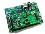


 工商网监
湘ICP备2023018690号
工商网监
湘ICP备2023018690号
