User's Guide
SLAU632B – October 2015 – Revised July 2018
ADS52J90 8/16/32-Channel, Analog-to-Digital Converter
Evaluation Module
This user’s guide gives an overview of the evaluation module (EVM) and provides a general description of
the features and functions to be considered while using this module. This manual is applicable to the
ADS52J90 analog-to-digital converters (ADC). The ADS52J90 EVM provides a platform for evaluating the
ADC under various signal, clock, reference, and ADC output formats. In addition, the EVM supports the
testing of both an LVDS interface as well as a JESD204B interface.
NOTE: A different capture card EVM is required for each interface.
NOTE: In compliance with the Article 33 provision of the EU REACH regulation, we are notifying you
that this EVM includes component(s) that contain at least one Substance of Very High
Concern (SVHC) above 0.1%. These uses from Texas Instruments do not exceed 1 ton per
year. The SVHC's are listed in Table 1:
Table 1. List of SVHCs
1
2
3
4
5
Component Manufacturer
Component Part Number
SVHC Substance
SVHC CAS (When Available)
Abracon ABM8G
ABM8G
Diboron trioxide
1303-86-2
Abracon ABM8G
ABM8G
Lead oxide
1317-36-8
Contents
Quick Views of Evaluation Setups for LVDS and JESD204B Interfaces ............................................. 3
1.1
LVDS Interface (ADS52J90 EVM + TSW1400)................................................................. 3
1.2
JESD204B Interface (ADS52J90 EVM + TSW14J56) ......................................................... 4
GUI Software Installation ................................................................................................... 5
2.1
High Speed Data Converter Pro (HSDCpro) GUI Installation ................................................ 5
2.2
ADS52J90 GUI Installation (HMC-DAQ)......................................................................... 5
ADS52J90 EVM Headers/Test Points and Clock Configuration ....................................................... 6
3.1
ADS52J90 EVM Header Configuration .......................................................................... 6
3.2
ADS52J90 EVM Test points ....................................................................................... 7
3.3
EVM Clock Configuration .......................................................................................... 8
Quick Test LVDS Interface ................................................................................................. 9
4.1
EVM Layout and Hardware Setup ................................................................................ 9
4.2
Capturing Ramp Test Pattern and Sinusoidal Input .......................................................... 12
4.3
Testing All Modes of the Device................................................................................. 24
Hardware Reference ....................................................................................................... 27
5.1
Bill of Materials .................................................................................................... 27
5.2
Schematics ......................................................................................................... 34
List of Figures
1
2
3
....................................................................................................
JESD204B Evaluation Setup ..............................................................................................
Clock Config: LMK CDM Mode ...........................................................................................
LVDS Evaluation Setup
SLAU632B – October 2015 – Revised July 2018
Submit Documentation Feedback
ADS52J90 8/16/32-Channel, Analog-to-Digital Converter Evaluation Module
Copyright © 2015–2018, Texas Instruments Incorporated
3
4
8
1
�www.ti.com
4
5
6
7
8
9
10
11
12
13
14
15
16
17
18
19
20
21
22
23
24
25
26
27
28
29
30
31
32
33
34
35
36
37
38
....................................................................................... 9
HSDCpro 10x Lane Rate Message ....................................................................................... 9
ADS52J90 EVM Analog Channels ...................................................................................... 10
TSW1400 and ADS52J90 Setup ........................................................................................ 11
TSW1400 GUI Setup (a) ................................................................................................. 12
TSW1400 GUI Setup (b) ................................................................................................. 13
TSW1400 GUI Setup (c) ................................................................................................. 13
TSW1400 GUI Setup (d) .................................................................................................. 14
TSW1400 GUI Setup (e) ................................................................................................. 14
TSW1400 GUI Setup (f) .................................................................................................. 15
HMC-DAQ GUI Setup (a) ................................................................................................. 15
HMC-DAQ GUI Setup (b) ................................................................................................ 16
HMC-DAQ GUI Setup (c) ................................................................................................. 16
HMC-DAQ GUI Setup (d) ................................................................................................ 17
ADS52J90 16-Channel RAMP Capture (a) ............................................................................ 18
ADS52J90 16-Channel RAMP Capture (b) ............................................................................. 19
ADS52J90 16-Channel RAMP Capture (c) ............................................................................ 19
ADS52J90 16-Channel RAMP Capture (d) ............................................................................ 20
ADS52J90 16-Channel SINE Capture (a) .............................................................................. 21
ADS52J90 16-Channel SINE Capture (b) .............................................................................. 22
ADS52J90 16-Channel SINE Capture (c) .............................................................................. 23
ADS52J90 All Supported Configs ....................................................................................... 24
ADS52J90 All Supported Configs (b) ................................................................................... 25
ADS52J90 All Supported Configs (c) ................................................................................... 26
ADS52J90 EVM Schematic (Page 1).................................................................................... 34
ADS52J90 EVM Schematic (Page 2).................................................................................... 35
ADS52J90 EVM Schematic (Page 3).................................................................................... 36
ADS52J90 EVM Schematic (Page 4).................................................................................... 37
ADS52J90 EVM Schematic (Page 5).................................................................................... 38
ADS52J90 EVM Schematic (Page 6).................................................................................... 39
ADS52J90 EVM Schematic (Page 7).................................................................................... 40
ADS52J90 EVM Schematic (Page 8).................................................................................... 41
ADS52J90 EVM Schematic (Page 9).................................................................................... 42
ADS52J90 EVM Schematic (Page 10) .................................................................................. 43
ADS52J90 EVM Schematic (Page 11) .................................................................................. 44
HSDCpro 40x Lane Rate Message
List of Tables
1
List of SVHCs ................................................................................................................ 1
2
ADS52J90 Default Header Configuration
3
ADS52J90 EVM Test Points ............................................................................................... 7
4
Bill of Materials
................................................................................
.............................................................................................................
6
27
Trademarks
2
ADS52J90 8/16/32-Channel, Analog-to-Digital Converter Evaluation Module
SLAU632B – October 2015 – Revised July 2018
Submit Documentation Feedback
Copyright © 2015–2018, Texas Instruments Incorporated
�Quick Views of Evaluation Setups for LVDS and JESD204B Interfaces
www.ti.com
1
Quick Views of Evaluation Setups for LVDS and JESD204B Interfaces
The ADS52J90 EVM can be tested using an LVDS data interface or a JESD204B data interface.
1.1
LVDS Interface (ADS52J90 EVM + TSW1400)
As shown in Figure 1, mating the ADS52J90 EVM with a TSW1400 EVM allows testing using an LVDS
data interface.
Figure 1. LVDS Evaluation Setup
FPGA EVM: The TSW1400 high-speed LVDS de-serializer EVM is required for capturing data from the
ADS52J90EVM. Analysis of the captured data is possible using its graphical user interface (GUI) which is
called High Speed Data Converter Pro.
NOTE:
The same GUI is used to control the TSW14J56 capture card for supporting a JESD204B
data interface.
For more information pertaining to be TSW1400EVM, see:
http://focus.ti.com/docs/toolsw/folders/print/tsw1400evm.html.
Equipment: Signal generators (with low-phase noise) must be used as source of input signal and clock in
order to get the desired performance. Additionally, a band-pass filter (BPF) is required on the analog input
signal to attenuate the harmonics and noise from the generators.
SLAU632B – October 2015 – Revised July 2018
Submit Documentation Feedback
ADS52J90 8/16/32-Channel, Analog-to-Digital Converter Evaluation Module
Copyright © 2015–2018, Texas Instruments Incorporated
3
�Quick Views of Evaluation Setups for LVDS and JESD204B Interfaces
www.ti.com
Power Supply: A single +5-V supply powers the ADS52J90EVM through connectors located at J47 and
J48 or through an AC adaptor (not provided) at J46. The supply for the ADS52J90 device is derived from
this +5-V supply. The power supply must be able to source up to 1.5 A. The TSW1400 EVM is powered
through an AC adaptor provided with its EVM kit.
USB Interface to PC: The USB connections from the ADS52J90EVM and TSW1400EVM to the computer
are used for communication from the GUIs to the boards. Section 2 explains the High Speed Data
Converter Pro and ADS52J90 GUI installation procedures.
1.2
JESD204B Interface (ADS52J90 EVM + TSW14J56)
As shown in Figure 2, mating the ADS52J90 EVM with a TSW14J56 EVM allows testing using a
JESD204B data interface.
Figure 2. JESD204B Evaluation Setup
FPGA EVM: The TSW14J56 high-speed JESD204B de-serializer board is required for capturing data from
the ADS52J90EVM. Analysis of the captured data is possible using its graphical user interface (GUI)
which is called High Speed Data Converter Pro (note: the same GUI is used to control the TSW1400
capture card for supporting an LVDS data interface).
For more information pertaining to be TSW14J56EVM, see: http://www.ti.com/tool/tsw14j56evm
Equipment: Signal generators (with low-phase noise) must be used as source of input signal and clock in
order to get the desired performance. Additionally, a band-pass filter (BPF) is required on the analog input
signal to attenuate the harmonics and noise from the generator.
4
ADS52J90 8/16/32-Channel, Analog-to-Digital Converter Evaluation Module
SLAU632B – October 2015 – Revised July 2018
Submit Documentation Feedback
Copyright © 2015–2018, Texas Instruments Incorporated
�GUI Software Installation
www.ti.com
Power Supply: A single +5-V supply powers the ADS52J90EVM through connectors located at J47 and
J48 or through an AC adaptor (not provided) at J46. The supply for the ADS52J90 device is derived from
this +5-V supply. The power supply must be able to source up to 1.5 A. The TSW14J56 EVM is powered
through an AC adaptor provided with its EVM kit.
USB Interface to PC: The USB connections from the ADS52J90EVM and TSW14J56EVM to the
computer are used for communication from the GUIs to the boards. Section 2 explains the High Speed
Data Converter Pro and ADS52J90 GUI installation procedures.
2
GUI Software Installation
The ADS52J90 EVM and the de-serializing capture card EVM both require software installations. The
following two sections explain where to find and how to install the software properly. Ensure that no USB
connections are made to the EVMs until after the installations are complete.
2.1
High Speed Data Converter Pro (HSDCpro) GUI Installation
Download the High Speed Data Converter Pro GUI Installer (SLWC107) from the Texas Instruments
website (www.ti.com) and install per the instructions in its user’s guide (SLWU087).
NOTE: Version 3.1 or higher of HSDC Pro is required to test the ADS52J0. If an earlier version of
HSDC Pro is installed, please uninstall before installing the latest version.
TI recommends installing HSDC Pro before installing the ADS52J90 GUI and installing it in the default
location provided during installation.
2.2
ADS52J90 GUI Installation (HMC-DAQ)
The GUI used to control the ADS52J90 EVM is a suite that supports a family of devices. The GUI is called
Healthtech Multi-Channel Data Acquisition GUI, or, HMC-DAQ. Download and save the file HMCDAQ_GUI_INSTALLER_SLOC326.zip to a temporary location on the local PC hard drive. Once saved,
unzip the file and run the executable as administrator by right clicking on the file. Follow the instructions
provided during installation. TI recommends installing after HSDCpro has been installed and in the default
location provided during installation.
SLAU632B – October 2015 – Revised July 2018
Submit Documentation Feedback
ADS52J90 8/16/32-Channel, Analog-to-Digital Converter Evaluation Module
Copyright © 2015–2018, Texas Instruments Incorporated
5
�ADS52J90 EVM Headers/Test Points and Clock Configuration
3
www.ti.com
ADS52J90 EVM Headers/Test Points and Clock Configuration
This section describes the functions of the headers on the EVM. It also provides a list of test points on the
EVM that are useful for debug and general-use purposes. Finally, several options for providing clocks to
the EVM are described.
3.1
ADS52J90 EVM Header Configuration
The ADS52J90 EVM is flexible in its configurability through the use of 2- and 3-pin headers. Table 2
describes the purpose of all headers on the EVM and the default positions. With this configuration, all
required clocks for testing the LVDS or JESD204B interface are derived from a single reference clock
provided to SMA J75 to the LMK04826 clocking device installed at designator U2 on the EVM. The
LMK04826 is configured for Clock Distribution Mode (CDM) with the provided scripts.
Table 2. ADS52J90 Default Header Configuration
Jumper
Description
Power
Supply
ADS52J90
SYNC
Options
Jumper#
Jumper Name
Default Config
Circuit
Description
JP9
+3.3VCLK
Short pins 1-2
Clocks
Power supply XTAL1, XTAL2, OSC1, LMK04826
JP10
IOVDD_+3.3V
Short pins 1-2
SPI BUFFERS
Power supply for SPI level shifters and isolators
JP11
DVDD_+1.2V
Short pins 1-2
ADS52JD90
+1.2-V digital power supply for ADS52JD90
JP12
AVDD_+1.8V
Short pins 1-2
ADS52JD90
+1.8-V analog power supply for ADS52JD90
JP13
LVDD_+1.8V
Short pins 1-2
ADS52JD90
+1.8-V digital power supply for ADS52JD90
JP15
DISABLE
DNI
Regulator
Not used
JP16
5VIN
DNI
Regulator
Not used
JP33
n/a
Short pins 1-2
ADS52JD90 SYNC pin
Selects SYNC signal source to ADS52JD90: (1) Auxiliary signal determined by JP28
or (3) GUI via FTDI device
JP28
n/a
Short pins 1-2
ADS52JD90 SYNC pin
Selects auxiliary SYNC signal source to ADS52JD90: (1) SMA J50 or (3) FPGA via
pin 105 of connector J44B
JP2
SYNC
Short pins 1-2
LMK SYNC
Selects the source of SYNC signal into LMK042x clock device: (1) signal from SMA
J39, LMK_SYNC or (3) signal from FPGA at pin K22 of connector J43C
JP3
LMK_RB
Short pins 2-3
LMK Readback/Reset
Selects LMK RESET pin signal source: (1) LMK_DATA_OUT out to FDTI (3)
LMK_RESET in from FTDI
JP39
ADC_CLK_AUX
Short pins 1-2
ADS52J90 CLKP/M &
SYSREFP/M Source
Selects auxiliary CLKP/M signal source to ADS52JD90: (1) SMA J55, ADC_CLK or
(3) one of two on-board XTAL oscillators determined by JP8
JP40
ADC_CLK
Short pins 2-3
Selects signal source to CLKP/M of ADS52J90: (1) Auxiliary source from JP39 or (3)
LMK04826 output
JP41
ADC_SYSREF
Short pins 1-2
Selects signal source to CLKP/M of ADS52J90: (1) Auxiliary source from JP39 or (3)
LMK04826 output
LMK04826
Options
ADC_CLKP/M
SEL
XTAL Power
Supply
Options
JP4
OSC1_VDD
Open
JP5
XTAL1_VDD
Open
XTAL/OSC Power
Powers 10-MHz XTAL1
JP6
XTAL2_VDD
Open
Powers 40-MHz XTAL2
JP7
LMK_CLKIN1
Short pins 1-2
LMK CLKIN1
Selects signal source to CLKIN1 of LMK04826: (1) SMA J75, LMK_CLKIN1 or (3)
XTAL determined by JP8
Open
XTAL Oscillators
Selects XTAL source to JP7 and JP39: (1) 10MHz XTAL1 or (3) 40MHz XTAL2
Analog Inputs 8ch
mode
Selects between (1) 5-V power supply and (2) and GND for amplifier on channels 7,8
for 8ch mode
XTAL SEL
Analog
Inputs 8ch
mode
JP8
XTAL_SEL
JP700_7
n/a
Short pins 2-3
JP800_8
n/a
Short pins 2-3
Powers 100-MHz OSC1
Jumpers JP11, JP12, JP13 can be removed and individual power supplies given to these headers in
order to monitor the DC current consumed by the ADS52J90.
6
ADS52J90 8/16/32-Channel, Analog-to-Digital Converter Evaluation Module
SLAU632B – October 2015 – Revised July 2018
Submit Documentation Feedback
Copyright © 2015–2018, Texas Instruments Incorporated
�ADS52J90 EVM Headers/Test Points and Clock Configuration
www.ti.com
3.2
ADS52J90 EVM Test points
Table 3 lists all test points on the ADS52J90 EVM and their purposes.
Table 3. ADS52J90 EVM Test Points
Test
Point
Silkscreen
Circuit
Description
TP13
+5.0V_IN
Power supply
Main +5-V power supply to EVM
TP15
GND
Power supply
Ground reference for EVM
TP14
IOVDD3.3V
Power supply
Power supply for VCM generation
TP12
+3.3VCLK
Power supply
Power supply for LMK0482x and oscillators
TP16
4V
Power supply
Input supply to regulator at designator U11
TP17
AVDD_+1.8V
Power supply
Power supply to ADS52J90
TP18
LVDD_+1.8V
Power supply
Power supply to ADS52J90
TP19
FORCE_VCM
Analog inputs
Can provide external VCM to analog inputs by installing R108 and
uninstalling R110
TP20
FORCE_VREF
Analog inputs
Can provide external VREF to ADS52J90 by installing R109
TP1
VCM
Analog inputs
ADS52J90 output providing VCM to analog inputs
TP4
GTX_CLKP
LMK0428x output
GTX clock to FPGA on capture card
TP5
GTX_CLKM
LMK0428x output
GTX clock to FPGA on capture card
TP21
CLK_LAO_0P
LMK0428x output
Global clock to FPGA on capture card (typ. equals Fs)
TP22
CLK_LAO_0M
LMK0428x output
Global clock to FPGA on capture card (typ. equals Fs)
TP6
SYSREF_P
LMK0428x output
SYSREF clock to FPGA on capture card
TP7
SYSREF_M
LMK0428x output
SYSREF clock to FPGA on capture card
TP8
CLKP
LMK0428x output
Device clock (Fs) to DUT from LMK0482x
TP10
CLKM
LMK0428x output
Device clock (Fs) to DUT from LMK0482x
TP9
SYSREFP
LMK0428x output
SYSREF clock to DUT from LMK0482x
TP11
SYSREFM
LMK0428x output
SYSREF clock to DUT from LMK0482x
TP37
CLK_P
DET LAT EVM
Device clock (Fs) to DUT when Deterministic Latency EVM is used
TP38
CLK_M
DET LAT EVM
Device clock (Fs) to DUT when Deterministic Latency EVM is used
TP35
SYSREF_P
DET LAT EVM
SYSREF clock to DUT when Deterministic Latency EVM is used
TP36
SYSREF_M
DET LAT EVM
SYSREF clock to DUT when Deterministic Latency EVM is used
TP23
GND
GND
Ground reference for EVM
TP2
SYNCP_SERDES
JESD SYNC
Input JESD SYNC~ to ADS52J90 from FPGA
TP3
SYNCM_SERDES
JESD SYNC
Input JESD SYNC~ to ADS52J90 from FPGA
TPA0
SCLK
ADS52J90 SPI PIN
SPI clock input to ADS52J90
TPA1
SDATA
ADS52J90 SPI PIN
SPI data input to ADS52J90
TPA2
SEN
ADS52J90 SPI PIN
SPI enable input to ADS52J90
TPA3
SDOUT
ADS52J90 SPI PIN
SPI read back output from ADS52J90
TPA4
RESET
ADS52J90 PIN
RESET pin to ADS52J90
TPA5
PDN_GBL
ADS52J90 PIN
PDN_GBL pin of ADS52J90
TPA6
PDN_FAST
ADS52J90 PIN
PDN_FAST pin of ADS52J90
TPA7
SYNC_LVDS_FTDI ADS52J90 PIN
SYNC pin to ADS52J90 allowing for synchronized LVDS outputs
TPB0
LMK_CLK
LMK SPI PIN
SPI clock input to LMK0482x
TPB1
LMK_DATA_OUT
LMK SPI PIN
SPI read back output from LMK0482x
TPB2
LMK_DATA
LMK SPI PIN
SPI data input to LMK0482x
TPB3
LMK_SPI_EN
LMK SPI PIN
SPI enable input to LMK0482x
TPB4
LMK_RESET
LMK PIN
RESET pin to LMK0482x
TPB5
RSV_DIG
n/a
Reserved
TP24
GND
GND
Ground Reference for EVM
SLAU632B – October 2015 – Revised July 2018
Submit Documentation Feedback
ADS52J90 8/16/32-Channel, Analog-to-Digital Converter Evaluation Module
Copyright © 2015–2018, Texas Instruments Incorporated
7
�ADS52J90 EVM Headers/Test Points and Clock Configuration
3.3
www.ti.com
EVM Clock Configuration
The EVM should be shipped with jumpers setting the LMK04826 clocking device (U2) in clock distribution
mode. In this configuration shown in Figure 3, the LMK04826 acts as a clock buffer/divider on the external
input clock to SMA J75, LMK_CLKIN1. For LVDS mode, this input clock should be set to the desired
system clock required by the ADS52J90. To support the JESD204B interface, this input clock should be
set to 1/40 the SerDes line rate when the line rate is above 1Gbps and 1/10 the SerDes line rate when the
line rate is below 1Gbps. Put another way, the SerDes lane rate will be 10x the reference clock when the
calculated lane rate is below 1Gbps and will be 40x the reference clock when the calculated lane rate is
above 1Gbps. The HSDCpro GUI will report both the calculated lane rate and the required reference clock
each time the user changes the Output Data Rate value in the GUI. Figure 4 and Figure 5 show examples
of the message when lane rate is 40x the reference clock and when the lane rate is 10x the reference
clock, respectively. Configuration scripts for both 10x rate and 40x rate are provided in folders with the
appropriate suffix appended to the folder names.
Figure 3. Clock Config: LMK CDM Mode
8
ADS52J90 8/16/32-Channel, Analog-to-Digital Converter Evaluation Module
SLAU632B – October 2015 – Revised July 2018
Submit Documentation Feedback
Copyright © 2015–2018, Texas Instruments Incorporated
�Quick Test LVDS Interface
www.ti.com
Figure 4. HSDCpro 40x Lane Rate Message
Figure 5. HSDCpro 10x Lane Rate Message
4
Quick Test LVDS Interface
This section outlines the following:
• EVM Layout and Hardware Setup
• How to capture a RAMP and Sinusoidal Inputs for 16ch mode
• How to use scripts to measure all LVDS modes supported by the device
4.1
EVM Layout and Hardware Setup
The ADS52J90 supports 3 modes of operation with respect to the analog inputs: (1) 32-channel mode, (2)
16-channel mode, (3) 8-channel mode. Figure 6 shows the breakdown of the analog channels on the
EVM. Testing 32-channel mode is done using all Channels 1-24 on the EVM. Testing 16-channel mode is
done using the odd channels of 1-23 on the EVM. These are the vertically-mounted SMAs. Testing 8channel mode is done using Channels 7 and 8. Channel 7 is configured to accept a differential input to
SMA_CH7A and SMA_CH7 whereas Channel 8 is configured to convert a signal ended input to
SMA_CH8 into a differential signal via an amplifier.
SLAU632B – October 2015 – Revised July 2018
Submit Documentation Feedback
ADS52J90 8/16/32-Channel, Analog-to-Digital Converter Evaluation Module
Copyright © 2015–2018, Texas Instruments Incorporated
9
�Quick Test LVDS Interface
www.ti.com
Figure 6. ADS52J90 EVM Analog Channels
The connections shown in Figure 7 should be made for proper hardware setup.
NOTE: Testing the LVDS interface between the ADS52J90 EVM and the TSW1400 EVM can be
performed using a RAMP test pattern generated within the ADS52J90 device in lieu of the
signal source listed in item 7, in the following steps.
10
ADS52J90 8/16/32-Channel, Analog-to-Digital Converter Evaluation Module
SLAU632B – October 2015 – Revised July 2018
Submit Documentation Feedback
Copyright © 2015–2018, Texas Instruments Incorporated
�Quick Test LVDS Interface
www.ti.com
Figure 7. TSW1400 and ADS52J90 Setup
1. Mate the TSW1400 EVM at connector J3 to the ADS52J90 EVM at connector J44 through the high
speed ADC interface connector.
NOTE: The two standoffs closest to J3 on the TSW1400 must be removed. Also, the EVM kit
provides two supplementary standoffs that should be added to the remaining two standoffs
so that the two EVMs are properly aligned.
2. Connect a DC +5-V power supply output of the provided AC-to-DC power supply to J12 (+5V_IN) of
the TSW1400 EVM and the input of the power supply cable to a 110–230 VAC source.
3. Ensure that SW7 is set to ON position on TSW1400.
4. Connect a DC +5-V power supply across banana jacks J47 and J48 on the ADS52J90 EVM.
Alternatively, test points TP13 and TP15 can be used if alligator clip leads are available.
5. Connect the USB cable from the PC to J45 (USB) of the ADS52J90 EVM.
6. Connect the USB cable from the PC to J5 (USB_IF) of the TSW1400 EVM.
NOTE:
TI recommends that the PC USB port be able to support USB2.0. If unsure, always chose
the USB ports at the back of the PC chassis over ones located on the front or sides.
SLAU632B – October 2015 – Revised July 2018
Submit Documentation Feedback
ADS52J90 8/16/32-Channel, Analog-to-Digital Converter Evaluation Module
Copyright © 2015–2018, Texas Instruments Incorporated
11
�Quick Test LVDS Interface
www.ti.com
7. Supply an analog input signal to SMA J1 (SMA_CH1) of the ADS52J90 EVM (such as +16 dBm, 5.0
MHz).
NOTE:
A low phase noise signal source (such as R&S SMA100A) with a band pass filter is needed
in order to measure SNR values reported in the datasheet. Also, the instrument should have
a 10-MHz back panel reference port allowing for coherent sampling when phase locked with
the sampling clock signal.
8. Supply a reference clock to SMA J75 (LMK_CLKIN1) of the ADS52J90 EVM that is equal to the
desired system clock frequency. In the following examples 65 MHz is used as it supports all channel
modes of the device.
NOTE: A low phase noise, highly linear, signal source (such as RS SMA100A) is needed in order to
measure SNR values reported in the datasheet. Also, the instrument should have a 10-MHz
back panel reference port allowing for coherent sampling when phase locked with the analog
input clock signal
4.2
Capturing Ramp Test Pattern and Sinusoidal Input
1. With the hardware setup shown in Figure 7 established, launch the High Speed Data Converter Pro
GUI. The GUI should automatically detect the serial number of the TSW1400 EVM connected as
shown in Figure 8. Click on OK.
Figure 8. TSW1400 GUI Setup (a)
12
ADS52J90 8/16/32-Channel, Analog-to-Digital Converter Evaluation Module
SLAU632B – October 2015 – Revised July 2018
Submit Documentation Feedback
Copyright © 2015–2018, Texas Instruments Incorporated
�Quick Test LVDS Interface
www.ti.com
The message shown in Figure 9 will appear. Click OK.
Figure 9. TSW1400 GUI Setup (b)
If instead, the message shown in Figure 10 appears, it indicates that the USB connection to the
TSW1400 EVM is not present. Click OK, then establish a USB connection and repeat step 1.
Figure 10. TSW1400 GUI Setup (c)
SLAU632B – October 2015 – Revised July 2018
Submit Documentation Feedback
ADS52J90 8/16/32-Channel, Analog-to-Digital Converter Evaluation Module
Copyright © 2015–2018, Texas Instruments Incorporated
13
�Quick Test LVDS Interface
www.ti.com
2. Select a device firmware to load in the FPGA by clicking on the blue arrow in the upper left corner of
the HSDCpro GUI. Scroll down and select ADS52J90 as shown in Figure 11.
Figure 11. TSW1400 GUI Setup (d)
Click the Yes button to update the ADC firmware on the TSW1400 FPGA as depicted in Figure 12.
Figure 12. TSW1400 GUI Setup (e)
14
ADS52J90 8/16/32-Channel, Analog-to-Digital Converter Evaluation Module
SLAU632B – October 2015 – Revised July 2018
Submit Documentation Feedback
Copyright © 2015–2018, Texas Instruments Incorporated
�Quick Test LVDS Interface
www.ti.com
While the firmware is being loaded into the TSW1400 FPGA, the graphic shown in Figure 13 will
appear after which the device GUI (HMC-DAQ) will launch as shown in Figure 14.
Figure 13. TSW1400 GUI Setup (f)
Figure 14. HMC-DAQ GUI Setup (a)
SLAU632B – October 2015 – Revised July 2018
Submit Documentation Feedback
ADS52J90 8/16/32-Channel, Analog-to-Digital Converter Evaluation Module
Copyright © 2015–2018, Texas Instruments Incorporated
15
�Quick Test LVDS Interface
www.ti.com
If the GUI recognizes that hardware is connected, HMC-DAQ will show HW CONNECTED in green in
the border of the GUI as shown in Figure 15.
Figure 15. HMC-DAQ GUI Setup (b)
If instead, the message shown in Figure 16 appears, it indicates a USB connection issues between the
PC and the ADS52J90 EVM. Close HSDCpro, establish USB connections and restart from procedure
1.
Figure 16. HMC-DAQ GUI Setup (c)
16
ADS52J90 8/16/32-Channel, Analog-to-Digital Converter Evaluation Module
SLAU632B – October 2015 – Revised July 2018
Submit Documentation Feedback
Copyright © 2015–2018, Texas Instruments Incorporated
�Quick Test LVDS Interface
www.ti.com
3. At this point there should be two GUI’s running and connected, HSDCpro and HMC-DAQ which are
communicating behind the scenes. Anytime the ADS52J90 device configuration is updated, HSDCpro
is informed and the appropriate firmware updates are done automatically. To capture a RAMP test
pattern in LVDS, 16-channel, 14 bit, 14x serialization configuration, do the following as shown in
Figure 17:
a. Press DUT RESET button
b. Press Initialize Device button
c. Check the box next to LVDS 16ch 14x 14b
d. Check the box next to Ramp Test Pattern
Figure 17. HMC-DAQ GUI Setup (d)
SLAU632B – October 2015 – Revised July 2018
Submit Documentation Feedback
ADS52J90 8/16/32-Channel, Analog-to-Digital Converter Evaluation Module
Copyright © 2015–2018, Texas Instruments Incorporated
17
�Quick Test LVDS Interface
www.ti.com
4. Return to HSDCpro GUI and perform the following steps as shown in Figure 18 .
a. Change the plot type from Real FFT to Codes
b. Enter 65M in the field labeled ADC Output Data Rate
c. Press the Capture button.
Figure 18. ADS52J90 16-Channel RAMP Capture (a)
18
ADS52J90 8/16/32-Channel, Analog-to-Digital Converter Evaluation Module
SLAU632B – October 2015 – Revised July 2018
Submit Documentation Feedback
Copyright © 2015–2018, Texas Instruments Incorporated
�Quick Test LVDS Interface
www.ti.com
A RAMP capture should appear as shown in Figure 19.
Figure 19. ADS52J90 16-Channel RAMP Capture (b)
By default, Ch1 (16CH) is the first channel displayed. Use the drop-down menu shown in Figure 20 to
view any one 16 channels.
Figure 20. ADS52J90 16-Channel RAMP Capture (c)
SLAU632B – October 2015 – Revised July 2018
Submit Documentation Feedback
ADS52J90 8/16/32-Channel, Analog-to-Digital Converter Evaluation Module
Copyright © 2015–2018, Texas Instruments Incorporated
19
�Quick Test LVDS Interface
www.ti.com
Zooming into the waveform and changing the plot graphic (using the buttons to the upper right of
graph), as shown in Figure 21, is recommended to confirm that the RAMP waveform is correct with
each subsequent sample incremented 1 ADC code until max code of (2N) – 1 is reached, where N is
ADC resolution.
Figure 21. ADS52J90 16-Channel RAMP Capture (d)
20
ADS52J90 8/16/32-Channel, Analog-to-Digital Converter Evaluation Module
SLAU632B – October 2015 – Revised July 2018
Submit Documentation Feedback
Copyright © 2015–2018, Texas Instruments Incorporated
�Quick Test LVDS Interface
www.ti.com
5. To capture a sinusoidal input, return to the HMC-DAQ GUI and press the check box next to Analog
Input as shown in Figure 22.
Figure 22. ADS52J90 16-Channel SINE Capture (a)
SLAU632B – October 2015 – Revised July 2018
Submit Documentation Feedback
ADS52J90 8/16/32-Channel, Analog-to-Digital Converter Evaluation Module
Copyright © 2015–2018, Texas Instruments Incorporated
21
�Quick Test LVDS Interface
www.ti.com
6. Return to HSDCpro GUI and perform the following (as illustrated in Figure 23):
a. Change the plot type from Codes to Real FFT
b. Enter 65M in the field labeled ADC Output Data Rate
c. Enter 5.0M in the field labeled ADC Input Target Frequency (or set to the desired input that is
being provided to SMA J1, SMA_CH1, as described in (Section 4.1).
d. Press the Capture button.
Figure 23. ADS52J90 16-Channel SINE Capture (b)
22
ADS52J90 8/16/32-Channel, Analog-to-Digital Converter Evaluation Module
SLAU632B – October 2015 – Revised July 2018
Submit Documentation Feedback
Copyright © 2015–2018, Texas Instruments Incorporated
�Quick Test LVDS Interface
www.ti.com
A capture similar to that shown in Figure 24 should appear.
NOTE:
The analog input level was adjusted and a recapture done iteratively until the Fund. value
was approximately –1 dBFs.
Figure 24. ADS52J90 16-Channel SINE Capture (c)
By default, Ch1 (16CH) is the first channel displayed. Use the drop-down menu to view any one 16
channels.
NOTE: The vertically-mounted SMAs on the EVM are the analog inputs to the odd ADC channels
while the side-mounted SMAs are the analog inputs to the even ADC channels. Per the
datasheet, only odd channels are being sampled when in 16-channel mode.
SLAU632B – October 2015 – Revised July 2018
Submit Documentation Feedback
ADS52J90 8/16/32-Channel, Analog-to-Digital Converter Evaluation Module
Copyright © 2015–2018, Texas Instruments Incorporated
23
�Quick Test LVDS Interface
4.3
www.ti.com
Testing All Modes of the Device
In addition to the quick start buttons provided on the QUICK SETUP tab of HMC-DAQ GUI, there are
scripts to configure the device for all supported modes. To access the scripts, click on the folder icon in
the upper left corner of the HMC-DAQ GUI, as shown in Figure 25.
Figure 25. ADS52J90 All Supported Configs
24
ADS52J90 8/16/32-Channel, Analog-to-Digital Converter Evaluation Module
SLAU632B – October 2015 – Revised July 2018
Submit Documentation Feedback
Copyright © 2015–2018, Texas Instruments Incorporated
�Quick Test LVDS Interface
www.ti.com
Navigate to the folder …../Scripts/ADS52J90/LVDS/LMK_CDM_MODE as shown in Figure 26.
Figure 26. ADS52J90 All Supported Configs (b)
SLAU632B – October 2015 – Revised July 2018
Submit Documentation Feedback
ADS52J90 8/16/32-Channel, Analog-to-Digital Converter Evaluation Module
Copyright © 2015–2018, Texas Instruments Incorporated
25
�Quick Test LVDS Interface
www.ti.com
Select anyone of 24 configurations provided and then press Capture in HSDCpro. When testing 32channel mode, ensure that the ADC Output Data Rate in HSDCpro is set to half the system clock being
provided to the device. For example, if 65 MHz is supplied to J75 then this value should be set to 32.5
MHz. When testing 8-channel or 16-channel modes, the ADC Output Data Rate should be set to the
value of the system clock provided to the DUT.
Figure 27. ADS52J90 All Supported Configs (c)
26
ADS52J90 8/16/32-Channel, Analog-to-Digital Converter Evaluation Module
SLAU632B – October 2015 – Revised July 2018
Submit Documentation Feedback
Copyright © 2015–2018, Texas Instruments Incorporated
�Hardware Reference
www.ti.com
5
Hardware Reference
5.1
Bill of Materials
Table 4. Bill of Materials
Reference Designator
Quantity
Value
Description
Package
Reference
Part Number
Manufacturer
C1, C2, C4, C9, C12, C32, C70,
C77, C85, C94, C103, C112,
C117, C285, C286, C297, C298,
C805, C806, C807, C808, C809,
C810, C811, C812, C813, C814,
C815, C816, C817, C818, C819,
C820, C837
34
0.1uF
CAP, CERM, 0.1uF, 16V, +/-10%, X7R, 0402
0402
GRM155R71C104KA88D
MuRata
C3, C8
2
1uF
CAP, CERM, 1uF, 10V, +/-10%, X5R, 0402
0402
GRM155R61A105KE15D
MuRata
C5, C10
2
0.01uF
CAP, CERM, 0.01uF, 50V, +/-10%, X7R, 0402
0402
GRM155R71H103KA88D
MuRata
C6
1
3900pF
CAP, CERM, 3900pF, 50V, +/-10%, X7R, 0402
0402
GRM155R71H392KA01D
MuRata
C7
1
47pF
CAP, CERM, 47pF, 50V, +/-5%, C0G/NP0, 0402
0402
GRM1555C1H470JZ01
MuRata
Alternate Part
Number
Supplier 1
C11
1
0.68uF
CAP, CERAMIC, 0.68uF, 6.3V, -20%, +80%, Y5V,
0402
0402
GRM155F50J684ZE01D
MURATA
-
-
C31
1
10uF
CAP, CERAMIC, 10uF, 10V, 10%, X5R, 0603
0603
C1608X5R1A106K080AC
TDK
-
-
C45
1
0.01uF
CAP, CERAMIC, 0.01uF, 50V, 5%, X7R, 0603
0603
06035C103JAT2A
AVX
-
-
C49
1
10uF
CAP, TANT, 10uF, 16V, 10%, 2.8 OHM, 3528-21
3528-21
TAJB106K016RNJ
AVX
-
-
C50, C52, C54
3
4.7uF
CAP, TANT, 4.7uF, 16V, 10%, 4 OHM, 3216-18
3216-18
TAJA475K016RNJ
AVX
-
-
C51, C55, C289, C290, C291,
C292
6
0.1uF
CAP, CERAMIC, 0.1uF, 16V, 10%, X5R, 0402
0402
EMK105BJ104KV-F
TAIYO YUDEN
-
-
MuRata
-
-
-
-
C53
1
0.01uF
CAP, CERM, 0.01uF, 25V, +/-10%, X7R, 0402
0402
GRM155R71E103KA01D
C56, C57
2
100uF
CAP, CERAMIC, 100uF, 6.3V, 20%, X5R, 1206
1206
C1206C107M9PACTU
KEMET
C58, C853
2
10uF
CAP, CERM, 10uF, 6.3V, +/-20%, X5R, 0603
0603
GRM188R60J106ME47D
MuRata
C61, C62
2
27pF
CAP, CERAMIC, 27pF, 250V, 2%, NPO, 0603
0603
251R14S270GV4T
JOHANSON TECHNOLOGY INC
C63, C64, C65, C66, C67, C68,
C69, C700_7, C701_7, C701a_7,
C800_8, C801_8
12
0.1uF
CAP, CERM, 0.1uF, 16V, +/-10%, X7R, 0603
0603
GRM188R71C104KA01D
MuRata
C72, C82, C96, C98, C107, C114,
C116, C120
8
1uF
CAP, CERM, 1uF, 25V, +/-10%, X7R, 0603
0603
C1608X7R1E105K080AB
TDK
C73, C97, C115
3
47uF
CAP, CERAMIC, 47uF, 10V, 20%, X5R, 1206
1206
GRM31CR61A476ME15L
MURATA
-
-
C74, C79, C102, C111
4
10uF
CAP, CERAMIC, 10uF, 25V, 10%, X5R, 0805
0805
GRM21BR61E106KA73L
MURATA
-
-
C75, C76, C83, C84
4
0.01uF
CAP, CERM, 0.01uF, 10V, +/-10%, X5R, 0402
0402
GRM155R61A103KA01D
MuRata
AVX
C78
1
47uF
CAP, TA, 47uF, 10V, +/-10%, 0.25 ohm, SMD
3528-21
TPSB476K010R0250
C80, C86, C104, C118
4
33uF
CAP, TA, 33uF, 16V, +/-10%, 0.35 ohm, SMD
3528-21
TPSB336K016R0350
AVX
C81, C87, C105, C119
4
10uF
CAP, CERAMIC, 10uF, 6.3V, 20%, X5R, 0805
0805
C2012X5R0J106M125AB
TDK CORPORATION
-
-
C88
1
0.1uF
CAP, CERAMIC, 0.1uF, 10V, 10%, X5R, 0402
0402
C0402C104K8PAC
KEMET
-
-
C89, C90
2
22uF
CAP, TA, 22uF, 16V, +/-10%, 0.375 ohm, SMD
6032-28
TPSC226K016R0375
AVX
-
-
C92
1
10uF
CAP, CERM, 10uF, 25V, +/-10%, X5R, 1206
1206
GRM31CR61E106KA12L
MuRata
C93, C106
2
0.1uF
CAP, CERAMIC, 0.1uF, 16V, 10%, X7R, 0603
0603
0603YC104KAT2A
AVX
C99, C100, C101
3
22uF
CAP, CERM, 22uF, 10V, +/-20%, X5R, 1210
1210
C3225X5R1A226M
TDK
SLAU632B – October 2015 – Revised July 2018
Submit Documentation Feedback
ADS52J90 8/16/32-Channel, Analog-to-Digital Converter Evaluation Module
Copyright © 2015–2018, Texas Instruments Incorporated
27
�Hardware Reference
www.ti.com
Table 4. Bill of Materials (continued)
Description
Package
Reference
Part Number
Manufacturer
Alternate Part
Number
Supplier 1
0.01uF
CAP, CERAMIC, 0.01uF, 25V, 10%, X7R, 0603
0603
C1608X7R1E103K080AA
TDK
-
-
3300pF
CAP, CERAMIC, 3300pF, 50V, 10%, X7R, 0603
0603
06035C332KAT2A
AVX
-
-
1uF
CAP, CERM, 1uF, 10V, +/-10%, X5R, 0603
0603
C0603C105K8PACTU
Kemet
108
0.1uF
'CAP, CERAMIC, 0.1uF, 16V, 10%, X7R, 0402
402
0402YC104KAT2A
AVX
-
-
Reference Designator
Quantity
C109
1
C110
1
C121
1
C122, C123, C124, C127, C128,
C129, C130, C131, C132, C133,
C134, C137, C138, C139, C140,
C141, C142, C143, C144, C147,
C148, C149, C150, C151, C152,
C153, C154, C157, C158, C159,
C160, C161, C162, C163, C164,
C167, C168, C169, C170, C171,
C172, C173, C174, C177, C178,
C179, C180, C181, C182, C183,
C184, C187, C188, C189, C190,
C191, C192, C193, C194, C197,
C198, C199, C200, C201, C202,
C203, C204, C207, C208, C209,
C210, C211, C212, C213, C214,
C217, C218, C219, C220, C221,
C222, C223, C224, C227, C228,
C229, C230, C231, C232, C233,
C234, C237, C238, C239, C240,
C241, C242, C673, C674, C675,
C678, C680, C821, C848, C849,
C858, C858a, C859
Value
C701
1
1000pF
CAP, CERAMIC, 1000pF, 50V, 10%, X7R, 0402
0402
ECJ-0EB1H102K
PANASONIC
C702_7, C703_7, C704_7,
C802_8, C803_8, C804_8
6
0.22uF
CAP, CERM, 0.22 µF, 25 V, +/- 10%, X5R, 0603
0603
06033D224KAT2A
AVX
C706_7, C707_7, C806_8,
C807_8
4
0.01uF
CAP, CERM, 0.01 µF, 50 V, +/- 10%, X7R, 0603
0603
C1608X7R1H103K
TDK
C712_7, C812_8
2
0.1uF
CAP, CERM, 0.1 µF, 50 V, +/- 10%, X7R, 0603
0603
06035C104KAT2A
AVX
C713_7, C813_8
2
33pF
CAP, CERM, 33pF, 50V, +/-5%, C0G/NP0, 0603
0603
GRM1885C1H330JA01D
MuRata
C801
1
10uF
CAP, CERAMIC, 10uF, 6.3V, 20%, X5R, 0603
0603
JMK107BJ106MA-T
TAIYO YUDEN
-
-
C830, C833, C838
3
0.1uF
CAP, CERAMIC, 0.1uF, 16V, 10%, X7R, 0402
0402
GRM155R71C104KA88
MURATA
-
-
C850, C851
2
0.01uF
CAP, CERM, 0.01uF, 25V, +/-10%, X7R, 0402
0402
C1005X7R1E103K
TDK
C854, C855
2
100pF
CAP, CERAMIC, 100pF, 50V, 5%, C0G, 0402
0402
GRM1555C1H101JZ01D
MURATA
-
-
C856
1
10pF
CAP, CERAMIC, 10pF, 50V, 5%, C0G, 0402
0402
GRM1555C1H100JZ01D
MURATA
-
-
C857
1
2200pF
CAP, CERAMIC, 2200pF, 50V, 10%, X7R, 0402
0402
GRM155R71H222KA01D
MURATA
-
-
D1, D2, D3, D4, D5, D6, D7, D8
8
GREEN
LED, GREEN CLEAR, 1206 SMD
1206
LTST-C150KGKT
LITE-ON INC
-
-
D9
1
15V
Diode, Schottky, 15V, 25A, DDPAK
DDPAK
MBRB2515LT4G
ON Semiconductor
FB1, FB2, FB3, FB4, FB5, FB6,
FB7, FB8, FB9, FB543
10
120
FERRITE BEAD, 120 OHM, 25% , 3500 mA, 0.02
OHM, SMT-1206
1206
BLM31PG121SN1L
MURATA
-
-
FERRITE BEAD, 1K OHM, 25% , 200 mA, 0.65
OHM, SMT-0402
0402
BLM15AG102SN1D
MURATA
-
-
HI1206P121R-10
Laird-Signal Integrity Products
28
FB10
1
1K
FB13, FB14, L2, L3
4
120 ohm
Ferrite Bead, 120 ohm @ 100 MHz, 4 A, 1206
1206
80 OHM
FERRITE BEAD, 80 OHM AT 100 MHZ, 5A, 0.01
OHM, SMT0805
FB15
1
0805
HI0805R800R-10
LAIRD TECH
-
-
FB16, FB17
2
FILTER, LC HIGH FREQ, 27UF, SMD 1206
1206
NFM31PC276B0J3
MURATA
-
-
H1, H2
2
HEX STANDOFF 6-32 ALUMINUM 1/2
Standoff
8414
Keystone
-
-
ADS52J90 8/16/32-Channel, Analog-to-Digital Converter Evaluation Module
Copyright © 2015–2018, Texas Instruments Incorporated
SLAU632B – October 2015 – Revised July 2018
Submit Documentation Feedback
�Hardware Reference
www.ti.com
Table 4. Bill of Materials (continued)
Description
Package
Reference
Part Number
Manufacturer
Alternate Part
Number
Supplier 1
16
Connector, 50 OHM, TH, SMA, ROHS
-
SMA-J-P-H-ST-TH1
SAMTEC
-
-
J2, J4, J6, J8, J10, J12, J14, J16,
J18, J20, J22, J24
12
CONNECTOR, SMA JACK, 50 OHM, EDGE
MOUNT
-
142-0711-821
EMERSON CONNECTIVITY
-
-
J39
1
Connector, TH, SMA
SMA
142-0701-201
Emerson Network Power
J43
1
Connector, Receptacle, 400-Pos (40x10), 50x50-mil
Pitch, SMT
2196x280x478
mil
ASP-134488-01
Molex
45970-4315
Molex
J44
1
CONNECTOR, HEADER, 120 POS, SMT
-
QTH-060-02-F-D-A
SAMTEC
-
-
67803-8020
Molex
Reference Designator
Quantity
J1, J3, J5, J7, J7_7, J7a_7, J8_8,
J8a_8, J9, J11, J13, J15, J17,
J19, J21, J23
Value
J45
1
Connector, Receptacle, USB - mini AB, R/A, SMD
Receptacle, 5Leads, Body
9.9x9mm, R/A
J46
1
Power Jack, mini, 2.1mm OD, R/A, TH
Jack,
14.5x11x9mm
RAPC722X
Switchcraft
J47
1
BANANA JACK, INSULATED, SOLDER LUG, RED
COLOR, TH-1P
-
SPC15363
TENMA
-
J48
1
BANANA JACK, INSULATED, SOLDER LUG,
BLACK COLOR, TH-1P
-
SPC15354
TENMA
-
J50, J55, J75, J76
4
CONN, SMA, JACK, 2.54 MM PITCH, STRAIGHT,
THRU
-
901-144-8RFX
AMPHENOL
-
-
JP2, JP3, JP6, JP7, JP8, JP28,
JP33, JP700_7, JP800_8
9
CONN, HEADER, 3POS, .100", T/H GOLD
-
HTSW-103-07-G-S
SAMTEC
-
-
JP4, JP5, JP9, JP10, JP11, JP12,
JP13
7
CONN, MALE, STRAIGHT, 2.54 MM PITCH, 2-PIN,
THRU
-
HMTSW-102-07-G-S-240
SAMTEC
-
-
JP39, JP40, JP41
3
Header, TH, 100mil, 3x2, Gold plated, 230 mil
above insulator
3x2 Header
TSW-103-07-G-D
Samtec
L1
1
1K OHM
FERRITE CHIP, EMIFIL, 1K OHM AT 100 MHZ,
500mA, 0.28 ohm, SMT0805
0805
BLM21AG102SN1D
MURATA
-
-
L4
1
1.5uH
Inductor, Shielded, Composite, 1.5uH, 7.12A, 0.02
ohm, SMD
4x2.1x4mm
XAL4020-152MEB
Coilcraft
MT1, MT2, MT3, MT4, MT5
5
Threaded Standoffs
-
2205
KEYSTONE
-
-
OSC1
1
OSCC, VCXO CMOS, 100.0 MHZ ,3.3V, +/-20ppm,
SMT, 4P
-
CVHD-950-100.000
CRYSTEK CORPORATION
-
-
100.00 MHZ
Q1
1
30V
MOSFET, N-CH, 30V, 5A, SON 2x2mm
SON 2x2mm
CSD17313Q2
Texas Instruments
R13, R14, R91
3
1K OHM
RESISTOR, THICK FILM, 1K OHM, 1%, 0.1W,
SMT0402
0402
ERJ-2RKF1001X
PANASONIC
-
-
R16
1
620
RESISTOR, THICK FILM, 620 OHM, 5%, 0.1W,
SMT0402
0402
ERJ-2GEJ621X
PANASONIC
-
-
R18
1
39K
RESISTOR, THICK FILM, 39K OHM, 5%, 0.1W,
SMT0402
0402
ERJ-2GEJ393X
PANASONIC
-
-
R39, R40, R43, R45, R61, R63,
R64
7
750
RES, 750 ohm, 1%, 0.1W, 0603
0603
CRCW0603750RFKEA
Vishay-Dale
R44, R46, R88, R90, R92, R93,
R95, R338, R339, R592, R593,
R595, R687
13
0
RESISTOR, THICK FILM, 0 OHM, JUMPER, 0.1W,
SMT0402
0402
ERJ-2GE0R00X
Panasonic
R55, R75, R79, R80, R81
5
10K OHM
RESISTOR, THICK FILM, 10K OHM, 1%, 0.1W,
SMT0402
0402
ERJ-2RKF1002X
PANASONIC
-
-
R67, R68
2
10.0
RES, 10.0 ohm, 1%, 0.1W, 0603
0603
RC0603FR-0710RL
Yageo America
SLAU632B – October 2015 – Revised July 2018
Submit Documentation Feedback
None
ADS52J90 8/16/32-Channel, Analog-to-Digital Converter Evaluation Module
Copyright © 2015–2018, Texas Instruments Incorporated
29
�Hardware Reference
www.ti.com
Table 4. Bill of Materials (continued)
Reference Designator
Quantity
Value
Description
Package
Reference
Part Number
Manufacturer
Alternate Part
Number
Supplier 1
R71
1
12K
RESISTOR, THICK FILM, 12K OHM, 1%, 0.1W,
SMT0603
0603
ERJ-3EKF1202V
PANASONIC
-
-
R72
1
4.7K OHM
RESISTOR, THICK FILM, 4.7K OHM, 1%, 0.1W,
SMT0402
0402
ERJ-2RKF4701X
PANASONIC
-
-
0603
ERJ-3EKF1001V
PANASONIC
-
-
-
-
R74
1
1K
RESISTOR, THICK FILM, 1K OHM, 1%, 0.1W,
SMT0603
R84
1
2.2K OHM
RESISTOR, THICK FILM, 2.2K OHM, 1%, 0.1W,
SMT0402
0402
ERJ-2RKF2201X
PANASONIC
R96
1
30k
RES, 30k ohm, 5%, 0.063W, 0402
0402
CRCW040230K0JNED
Vishay-Dale
R98, R102
2
100K
RESISTOR, THICK FILM, 100K OHM, 1%, 0.1W,
SMT0603
0603
ERJ-3EKF1003V
PANASONIC
-
-
R103
1
26.1K
RESISTOR, THICK FILM, 26.1K OHM, 1%, 0.1W,
SMT0603
0603
ERJ-3EKF2612V
PANASONIC
-
-
0603
ERJ-3EKF6653V
PANASONIC
-
-
-
-
R104
1
665K
RESISTOR, THICK FILM, 665K OHM, 1%, 0.1W,
SMT0603
R105
1
7.68K
RESISTOR, THICK FILM, 7.68K OHM, 1%, 0.1W,
SMT0603
0603
ERJ-3EKF7681V
PANASONIC
R110, R111, R112, R123, R124,
R125, R126, R137, R138, R139,
R140, R151, R152, R153, R154,
R165, R166, R167, R168, R179,
R180, R181, R182, R193, R194,
R195, R196, R207, R208, R209,
R210, R221, R222, R223, R224,
R235, R236, R237, R238, R249,
R250, R251, R252, R263, R264,
R265, R266, R277, R278,
R822_8, R823_8
51
10.0
RES, 10.0 ohm, 1%, 0.063W, 0402
0402
CRCW040210R0FKED
Vishay-Dale
R115, R116, R119, R120, R129,
R130, R133, R135, R143, R144,
R147, R148, R157, R158, R161,
R162, R171, R172, R175, R177,
R185, R186, R189, R190, R199,
R200, R203, R205, R212, R214,
R217, R219, R227, R228, R231,
R232, R241, R242, R245, R246,
R255, R256, R259, R260, R269,
R270, R273, R274
48
24.9
RES, 24.9 ohm, 1%, 0.063W, 0402
0402
CRCW040224R9FKED
Vishay-Dale
R520, R521, R524, R525, R686
5
49.9
RESISTOR, THICK FILM, 49.9 OHM, 1%, 0.1W,
SMT0402
0402
ERJ-2RKF49R9X
PANASONIC
-
-
R602, R603, R682, R683, R684,
R696
6
100
RESISTOR, THICK FILM, 100 OHM, 1%, 0.1W,
SMT0402
0402
ERJ-2RKF1000X
PANASONIC
-
-
R604, R605, R606
3
100
RES, 100 ohm, 5%, 0.063W, 0402
0402
CRCW0402100RJNED
Vishay-Dale
R634, R698
2
10k
RES, 10k ohm, 5%, 0.125W, 0805
0805
ERJ-6GEYJ103V
Panasonic
-
-
30
R685
1
0
RESISTOR, THICK FILM, 0 OHM, JUMPER,
0.063W, SMT0402
0402
CRCW04020000Z0ED
VISHAY
R706_7, R707_7
2
0
RES, 0, 5%, 0.063 W, 0402
0402
CRCW04020000Z0ED
Vishay-Dale
R708_7, R709_7, R722_7,
R723_7, R824_8, R825_8,
R826_8, R827_8
8
0
RES, 0, 1%, 0.063 W, 0402
0402
RC0402JR-070RL
Yageo America
R710_7, R711_7, R810_8,
R811_8
4
15.0
RES, 15.0, 1%, 0.1 W, 0603
0603
CRCW060315R0FKEA
Vishay-Dale
ADS52J90 8/16/32-Channel, Analog-to-Digital Converter Evaluation Module
Copyright © 2015–2018, Texas Instruments Incorporated
SLAU632B – October 2015 – Revised July 2018
Submit Documentation Feedback
�Hardware Reference
www.ti.com
Table 4. Bill of Materials (continued)
Reference Designator
Quantity
Value
Description
Package
Reference
Part Number
Manufacturer
R712_7, R713_7, R714_7,
R715_7, R716_7, R717_7,
R812_8, R813_8, R814_8,
R815_8, R816_8, R817_8
12
0
RES, 0, JUMPER, 0.1 W, 0603
0603
ERJ-3GEY0R00V
Panasonic
R718_7, R719_7, R818_8,
R819_8
4
24.9
RES, 24.9, 1%, 0.1 W, 0603
0603
CRCW060324R9FKEA
Vishay-Dale
R802_8
1
49.9
RES, 49.9, 1%, 0.063 W, 0402
0402
CRCW040249R9FKED
Vishay-Dale
R804_8, R805_8
2
64.9
RES, 64.9, 1%, 0.063 W, 0402
0402
CRCW040264R9FKED
Vishay-Dale
R806_8, R807_8
2
169
RES, 169, 1%, 0.063 W, 0402
0402
CRCW0402169RFKED
Vishay-Dale
R808_8, R809_8
2
348
RES, 348, 1%, 0.063 W, 0402
0402
CRCW0402348RFKED
Vishay-Dale
SHUNT_JP2, SHUNT_JP3,
SHUNT_JP4, SHUNT_JP5,
SHUNT_JP6, SHUNT_JP7,
SHUNT_JP8, SHUNT_JP9,
SHUNT_JP10, SHUNT_JP11,
SHUNT_JP12, SHUNT_JP13,
SHUNT_JP28, SHUNT_JP33,
SHUNT_JP88_1,
SHUNT_JP88_2,
SHUNT_JP89_1,
SHUNT_JP89_2,
SHUNT_JP506_1,
SHUNT_JP506_2,
SHUNT_JP700_7,
SHUNT_JP800_8
22
MJ-5.97-G OR EQUIVALENT
KELTRON
SW1
1
SW2, SW3
Alternate Part
Number
Supplier 1
SWITCH, TACTILE SPST-NO, 0.05A, 12 VDC, TH2 PIN
-
PTS635SL43LFS
C&K COMPONENTS
-
-
2
Switch, Push Button, SMD
2.9x2x3.9mm
SMD
SKRKAEE010
Alps
Equivalent
Any
T1, T2, T3, T4, T5, T6, T7, T8,
T9, T10, T11, T12, T13, T14, T15,
T16, T17, T18, T19, T20, T21,
T22, T23, T24
24
TRANSFORMER, RF, 50 OHM, 0.03 TO 125 MHZ,
6-PIN, SMT, ROHS
-
ADT1-6T
MINI-CIRCUITS
-
-
TADC_CLK, TSYSREF
2
TRANSFORMER, RF, 50 OHM, 2 MHZ TO 755
MHZ, 6-PIN, ROHS
-
ADT4-1WT
MINI-CIRCUITS
-
-
TP1, TP2, TP3, TP8, TP9, TP10,
TP11, TP13, TP15, TP19, TP20,
TP23, TP24, TP35, TP36, TP37,
TP38, TP111, TPA0, TPA1,
TPA2, TPA3, TPA4, TPA5, TPA6,
TPA7, TPB0, TPB1, TPB2, TPB3,
TPB4, TPB5
32
Black
Test Point, Miniature, Black, TH
Black Miniature
Testpoint
5001
Keystone
TP4, TP5, TP6, TP7, TP21, TP22,
TP25, TP26
8
White
Test Point, Miniature, White, TH
White Miniature
Testpoint
5002
Keystone
TP12, TP14, TP17, TP18, TP141
5
Blue
Test Point, Miniature, Blue, TH
Blue Miniature
Testpoint
5117
Keystone
BGA-198 , MULTI-CHANNEL HIGH SPEED ADC
WITH JESD204B INTERFACE
-
ADS52J90ZZE
TEXAS INSTRUMENTS
-
-
12 V
U1
1
U2
1
NKD0064A
LMK04826BISQ/NOPB
Texas Instruments
U4
1
IC, INVERT SCHMITT-TRIG, SC70-5
DCK
SN74AUP1T14DCK
TEXAS INSTRUMENTS
-
-
U5
1
IC, REG LDO, 3.3V, 0.1A, SOT23-5
DBV
TPS76933DBV
TEXAS INSTRUMENTS
-
-
SLAU632B – October 2015 – Revised July 2018
Submit Documentation Feedback
None
ADS52J90 8/16/32-Channel, Analog-to-Digital Converter Evaluation Module
Copyright © 2015–2018, Texas Instruments Incorporated
31
�Hardware Reference
www.ti.com
Table 4. Bill of Materials (continued)
Description
Package
Reference
Part Number
Manufacturer
1
Quad High Speed USB to Multipurpose
UART/MPSSE IC
LQFP_10x10m
m
FT4232HL
FTDI
Reference Designator
Quantity
U6
Value
Alternate Part
Number
Supplier 1
U7
1
IC, EEPROM, 1KBIT, 2MHZ, 8-SOIC
SN
93LC46BT-I/SN
MICROCHIP TECHNOLOGY
-
-
U8, U11, U13
3
IC, REG LDO, ADJ, 1A, 20-VQFN
RGW
TPS7A4700RGW
TEXAS INSTRUMENTS
-
-
U9
1
IC, OVERVOLT PROT CTRLR, SOT23-5
DBV
TPS2400DBV
TEXAS INSTRUMENTS
-
-
U10
1
IC, ULTRALOW-NOISE, HIGH PSRR, FAST, RF,
1A LOW-DROPOUT LINEAR REGULATORS,
SOT223-6
DCQ
TPS79601DCQ
TEXAS INSTRUMENTS
-
-
U12
1
IC, REG, BUCK, SYNC, ADJ, 3A, 16-WQFN
RTE
TPS54319RTE
TEXAS INSTRUMENTS
-
-
U14
1
IC, BUS, TXRX, TRI-ST, 2BIT, SM-8
DCT
SN74AVC2T45DCT
TEXAS INSTRUMENTS
-
-
U15
1
150 Mbps Quad Channels, 3 / 1, Digital Isolator, -40
to +125 degC, 16-pin SOIC (DW), Green (RoHS &
no Sb/Br)
DW0016A
ISO7241MDW
TEXAS INSTRUMENTS
Equivalent
None
U16, U18
2
IC, 4-BIT DUAL-SUPPLY BUS TRANSCEIVER
WITH CONFIGURABLE VOLTAGE TRANSLATION
AND 3-STATE OUTPUTS, TSSOP-16
PW
SN74AVC4T245PW
TEXAS INSTRUMENTS
-
-
U17
1
150 Mbps Quad Channels, 4 / 0, Digital Isolator, 3.3
V / 5 V, -40 to +125 degC, 16-pin SOIC (DW),
Green (RoHS & no Sb/Br)
DW0016A
ISO7240MDW
Texas Instruments
Equivalent
None
U800_8
1
IC,WIDEBAND, LOW-NOISE, LOW-DISTORTION,
FULLY-DIFFERENTIAL AMPLIFIER, 16-QFN
RGT
THS4509RGT
TEXAS INSTRUMENTS
XTAL1
1
OSCC, HCMOS, 3.3 V, +/-25 PPM, 10 MHZ, SMT,
6P
-
FXO-HC736R-10
FOX
-
-
XTAL2
1
OSC, 3.3 V, 40 MHz, SMD
SMD, 4-Leads,
Body 7x5mm
FXO-HC735-40
Fox Electronics
CRYSTAL 12.000MHZ 10PF SMD
3.2x0.55x2.5m
m
ABM8G-12.000MHZ-B4Y-T
Abracon Corportation
PMSSS 440 0075 PH
BUILDING FASTENERS
Y3
1
Z_SCREW1, Z_SCREW2,
Z_SCREW3, Z_SCREW4,
Z_SCREW5
5
10 MHZ
C13, C14, C15, C16, C17
0
0.01uF
CAP, CERM, 0.01uF, 50V, +/-10%, X7R, 0402
0402
GRM155R71H103KA88D
MuRata
C27, C29, C36, C37, C283, C284,
C287, C288
0
0.1uF
CAP, CERM, 0.1uF, 16V, +/-10%, X7R, 0402
0402
GRM155R71C104KA88D
MuRata
C59, C60
0
22pF
CAP, CERM, 22pF, 100V, +/-5%, C0G/NP0, 0603
0603
GRM1885C2A220JA01D
MuRata
C71, C91, C95, C113
0
4.7uF
CAP, TANTALUM, 4.7uF, 10%, 10V, SMT3528-21
3528-21
TAJB475K010RNJ
AVX
-
-
C108
0
3300pF
CAP, CERAMIC, 3300pF, 50V, 10%, X7R, 0603
0603
06035C332KAT2A
AVX
-
-
C125, C126, C135, C136, C145,
C146, C155, C156, C165, C166,
C175, C176, C185, C186, C195,
C196, C205, C206, C215, C216,
C225, C226, C235, C236
0
0.1uF
CAP, CERAMIC, 0.1uF, 16V, 10%, X7R, 0402
0402
0402YC104KAT2A
AVX
-
-
32
C705_7, C805_8
0
0.1uF
CAP, CERM, 0.1 µF, 50 V, +/- 10%, X7R, 0603
0603
06035C104KAT2A
AVX
C708_7, C709_7, C710_7,
C711_7, C808_8, C809_8,
C810_8, C811_8
0
1000pF
CAP, CERM, 1000 pF, 100 V, +/- 5%, C0G/NP0,
0603
0603
C1608C0G2A102J
TDK
C801a_8
0
0.1uF
CAP, CERM, 0.1uF, 16V, +/-10%, X7R, 0603
0603
GRM188R71C104KA01D
MuRata
F1
0
FUSE 2.0A 63V FAST
1206
1206SFF200F/63-2
TE Connectivity
ADS52J90 8/16/32-Channel, Analog-to-Digital Converter Evaluation Module
Copyright © 2015–2018, Texas Instruments Incorporated
SLAU632B – October 2015 – Revised July 2018
Submit Documentation Feedback
�Hardware Reference
www.ti.com
Table 4. Bill of Materials (continued)
Description
Package
Reference
0
Connector, TH, SMA
0
CONN, HEADER, 2POS, .100", T/H GOLD
Reference Designator
Quantity
J35, J36, J37, J38
JP15, JP16
L700_7, L701_7, L702_7,
L703_7, L800_8, L801_8,
L802_8, L803_8
0
Value
60nH
Part Number
Manufacturer
SMA
142-0701-201
Emerson Network Power
-
HTSW-102-08-G-S
SAMTEC
Inductor, Multilayer, 60nH, 3.37 A, 0.0219 ohm,
SMD
0603
MDT1608-CLHR06
Toko
Vishay-Dale
R1, R2, R5, R6, R9, R10
0
169
RES, 169 ohm, 1%, 0.063W, 0402
0402
CRCW0402169RFKED
R3, R4, R7, R8, R11, R12
0
49.9
RES, 49.9 ohm, 1%, 0.063W, 0402
0402
CRCW040249R9FKED
Vishay-Dale
R19, R20, R23, R24, R35, R36,
R41, R42, R47, R48
0
240 OHM
RESISTOR, THICK FILM, 240 OHM, 1%, 0.1W,
SMT0402
0402
ERJ-2RKF2400X
PANASONIC
R62, R94, R99, R101, R113,
R114, R121, R122, R127, R128,
R134, R136, R141, R142, R149,
R150, R155, R156, R163, R164,
R169, R170, R176, R178, R183,
R184, R191, R192, R197, R198,
R204, R206, R211, R213, R218,
R220, R225, R226, R233, R234,
R239, R240, R247, R248, R253,
R254, R261, R262, R267, R268,
R275, R276, R594
0
0
RESISTOR, THICK FILM, 0 OHM, JUMPER, 0.1W,
SMT0402
0402
ERJ-2GE0R00X
PANASONIC
R97, R100
0
0
RES, 0 ohm, 5%, 0.1W, 0603
0603
ERJ-3GEY0R00V
Panasonic
0603
ERJ-3EKF1002V
PANASONIC
R108
0
10K OHM
RESISTOR, THICK FILM, 10K OHM, 1%, 0.1W,
SMT0603
Alternate Part
Number
Supplier 1
-
-
-
-
-
-
R109
0
10.0
RES, 10.0 ohm, 1%, 0.063W, 0402
0402
CRCW040210R0FKED
Vishay-Dale
R117, R118, R131, R132, R145,
R146, R159, R160, R173, R174,
R187, R188, R201, R202, R215,
R216, R229, R230, R243, R244,
R257, R258, R271, R272
0
49.9
RESISTOR, THICK FILM, 49.9 OHM, 1%, 0.1W,
SMT0402
0402
ERJ-2RKF49R9X
PANASONIC
-
-
R673, R674, R678, R679
0
0
RESISTOR, THICK FILM, 0 OHM, JUMPER,
0.063W, SMT0402
0402
CRCW04020000Z0ED
VISHAY
-
-
R700_7, R701_7, R800_8,
R801_8
0
249
RES, 249, 1%, 0.063 W, 0402
0402
CRCW0402249RFKED
Vishay-Dale
R702_7
0
49.9
RES, 49.9, 1%, 0.063 W, 0402
0402
CRCW040249R9FKED
Vishay-Dale
R704_7, R705_7
0
64.9
RES, 64.9, 1%, 0.063 W, 0402
0402
CRCW040264R9FKED
Vishay-Dale
R720_7, R721_7, R820_8,
R821_8
0
49.9
RES, 49.9, 1%, 0.1 W, 0603
0603
CRCW060349R9FKEA
Vishay-Dale
R724_7, R725_7, R726_7,
R727_7
0
0
RES, 0, 1%, 0.063 W, 0402
0402
RC0402JR-070RL
Yageo America
Test Point, Miniature, Blue, TH
Blue Miniature
Testpoint
5117
Keystone
IC,WIDEBAND, LOW-NOISE, LOW-DISTORTION,
FULLY-DIFFERENTIAL AMPLIFIER, 16-QFN
RGT
THS4509RGT
TEXAS INSTRUMENTS
TP16
0
U700_7
0
Blue
Notes:
SLAU632B – October 2015 – Revised July 2018
Submit Documentation Feedback
d in the Alternate PartNumber and/or Alternate Manufacturer columns, all parts may be substituted with equivalents.
ADS52J90 8/16/32-Channel, Analog-to-Digital Converter Evaluation Module
Copyright © 2015–2018, Texas Instruments Incorporated
33
�Hardware Reference
5.2
www.ti.com
Schematics
1
2
3
4
5
6
7
8
ASD52J90 PINOUT
U1B
U1A
INP_9
INM_9
INP_11
INM_11
INP_13
INM_13
INP_15
INM_15
INP_17
INM_17
INP_19
INM_19
INP_21
INM_21
B
INP_23
INM_23
INP_25
INM_25
INP_27
INM_27
INP_29
INM_29
INP_31
INM_31
E2
E1
F2
F1
G2
G1
H2
H1
J2
J1
K2
K1
L2
L1
M2
M1
N2
N1
P2
P1
R2
R1
T2
T1
V2
V1
INP4
INM4
INP5
INM5
INP6
INM6
INP7
INM7
INP8
INM8
INP9
INM9
INP10
INM10
INP11
INM11
INP12
INM12
INP13
INM13
INP14
INM14
INP15
INM15
INP16
INM16
INP17
INM17
INP18
INM18
INP19
INM19
INP20
INM20
INP21
INM21
INP22
INM22
INP23
INM23
INP24
INM24
INP25
INM25
INP26
INM26
INP27
INM27
INP28
INM28
INP29
INM29
INP30
INM30
INP31
INM31
INP32
INM32
C3
D3
D2
D1
E4
E3
F4
F3
G4
G3
H4
H3
J4
J3
K4
K3
L4
L3
M4
M3
N4
N3
OUTPUTS
INP_2
INM_2
DOUTP1
DOUTM1
INP_4
INM_4
DOUTP2
DOUTM2
INP_6
INM_6
DOUTP3
DOUTM3
INP_8
INM_8
DOUTP4
DOUTM4
INP_10
INM_10
DOUTP5
DOUTM5
INP_12
INM_12
DOUTP6
DOUTM6
INP_14
INM_14
DOUTP7
DOUTM7
INP_16
INM_16
DOUTP8
DOUTM8
INP_18
INM_18
DOUTP9
DOUTM9
INP_20
INM_20
DOUTP10
DOUTM10
INP_22
INM_22
DOUTP11
DOUTM11
INP_24
INM_24
DOUTP12
DOUTM12
P4
P3
DOUTP13
DOUTM13
T3
R3
DOUTP14
DOUTM14
U2
U1
DOUTP15
DOUTM15
V3
U3
DOUTP16
DOUTM16
DOUT1P B9
DOUT1M B10
DOUT2P C9
DOUT2M C10
DOUT3P D9
DOUT3M D10
DOUT4P E9
DOUT4M E10
DOUT5P F9
DOUT5M F10
DOUT6P G9
DOUT6M G10
DOUT7P H9
DOUT7M H10
DOUT8P H11
DOUT8M G11
DOUT9P L11
DOUT9M M11
DOUTP1
DOUTM1
CML1_OUTP
CML1_OUTM
DOUTP2
DOUTM2
CML2_OUTP
CML2_OUTM
DOUTP3
DOUTM3
CML3_OUTP
CML3_OUTM
DOUTP4
DOUTM4
CML4_OUTP
CML4_OUTM
DOUTP5
DOUTM5
CML5_OUTP
CML5_OUTM
DOUTP6
DOUTM6
CML6_OUTP
CML6_OUTM
DOUTP7
DOUTM7
CML7_OUTP
CML7_OUTM
DOUTP8
DOUTM8
CML8_OUTP
CML8_OUTM
A9 CML1_OUTP
A10 CML1_OUTM
CML1_OUTP
CML1_OUTM
A11 CML2_OUTP
B11 CML2_OUTM
CML2_OUTP
CML2_OUTM
C11 CML3_OUTP
D11 CML3_OUTM
A
CML3_OUTP
CML3_OUTM
E11 CML4_OUTP
F11 CML4_OUTM
CML4_OUTP
CML4_OUTM
V9 CML5_OUTP
V10 CML5_OUTM
CML5_OUTP
CML5_OUTM
V11 CML6_OUTP
U11 CML6_OUTM
T11 CML7_OUTP
R11 CML7_OUTM
P11 CML8_OUTP
N11 CML8_OUTM
CML6_OUTP
CML6_OUTM
CML7_OUTP
CML7_OUTM
CML8_OUTP
CML8_OUTM
DOUTP9
DOUTM9
DOUT10P L9
DOUT10ML10
DOUTP10
DOUTM10
DOUT11P M9
DOUT11MM10
DOUTP11
DOUTM11
DOUT12P N9
DOUT12MN10
B
DOUTP12
DOUTM12
DOUT13P P9
DOUT13MP10
LVDD_+1.8V
JP33
DOUTP13
DOUTM13
DOUT14P R9
DOUT14MR10
DOUT16P U9
DOUT16MU10
3
ADC_SYNC_FTDI
DOUTP14
DOUTM14
DOUT15P T9
DOUT15MT10
SYNC
2
1
TP111
SYNC
DOUTP15
DOUTM15
FCLKP
FCLKM
DOUTP16
DOUTM16
DCLKP
DCLKM
J9 FCLKP
K9 FCLKM
FCLKP
FCLKM
J11 DCLKP
K11DCLKM
DCLKP
DCLKM
SYNC
3
2
1
J50
1
C
A8
J7
K7
K8
D7
K10
L7
L8
R6
H7
H8
J8
V8
E7
D
D5
P5
N5
AVSS
AVSS
AVSS
AVSS
AVSS
AVSS
AVSS
AVSS
AVSS
AVSS
AVSS
AVSS
AVSS
AVSS
AVSS
AVSS
AVSS
AVSS
POWER & GROUND
U1C
T5
V6
B4
H5
H6
U4
U6
R4
R5
J5
J6
C4
L5
L6
D4
T4
K5
K6
DVSS
DVSS
DVSS
DVSS
DVSS
DVSS
DVSS
DVSS
DVSS
DVSS
DVSS
DVSS
DVSS
DVSS
NC
NC
NC
AVDD
AVDD
AVDD
AVDD
AVDD
AVDD
AVDD
AVDD
AVDD
AVDD
ADC_CLK_M
ADC_CLK_P
AVDD_+1.8V
CLK from DET_LAT
V4
P6
G6
M6
A4
M5
F6
N6
G5
E6
10k
R2
R1
DNP DNP
169
169
DNI
DNI
C2
R338
R339
SYNCM_SERDES
SYNCP_SERDES
A7
N7
U8
V7
F7
B8
C8
G7
R8
T6
T8
M7
D8
R3
R4
DNP
49.9 DNP
49.9
R6 DNI
DNI
R5 DNP
DNP
169
169
DNI DNI
0
0
100
U1D
U5
V5
IOVDD_+3.3V
R7
DNP
49.9 R8
DNI DNP
49.9
R9
R10
DNI
DNP DNP
169
169
DNI
DNI
TP3
SYNCM TP2
SYNCP C285
0.1µF
C286
0.1µF
SYSREF from LMK
R605
P7
R7
100
T7
U7
R606
R11
R12
Share Pads for a T
TP9
DNP
C287DNP
49.9 DNP
49.9
SYSREFP
0.1µF
C288 DNI
DNI
TP11
DNI
DNP
SYSREFM
0.1µF
DNI
SYSREF_M
E8
J10
P8
M8
F8
G8
N8
R604
TP1
CLOCK/SPI/REF
JESD SYNC from FPGA
ADC_SYSREFM
ADC_SYSREFP
C
IOVDD_+3.3V
0.1µF
100
RESET
PDN_GBL
PDN_FAST
RSV_DIG
SYNC D6
A6
C7
C6
B6
CLKM
CLKP
VCM
REF VREF_IN
F5
E5
VCM
VREF_IN
SYNCM_SERDES
SYNCP_SERDES
SYSREFM_SERDES
SYSREFP_SERDES
SPI
SYNC
RESET
PDN_GBL
PDN_FAST
RESERVED_DIGITAL_PIN
SCLK
SDATA
SEN
SDOUT
B7
A5
B5
C5
SCLK
SDATA
SEN
SDOUT
ADS52J90
TP36
ADC_SYS_M
ADC_SYS_P
D
SYSREF from DET_LAT EVM
TP35
SYSREF_P
Mod. Date:5/21/2015
Designed for:
Texas Instruments and/or its licensors do not warra
nt the accuracy or completeness of this
Project: ADS52J90 EVM REV A
specification or any information contained therein.
Texas Instruments and/or its licensors do not
Sheet:2 of 11
Sheet Title:*
warrant that this design will meet the specificatio
ns, will be suitable for your application or rfit fo
Rev: A
Size: A3
Schematic:
any particular purpose, or will operate in an imple
mentation. Texas Instruments and/or its
Assembly Variant:001
licensors do not warrant that the design is product
ion worthy. You should completely validate
File: SHEET 2 - ADS52J90 PINOUT.SchDoc
and test your design implementation to confirm system
the
functionality for your application.
Contact: TechSupport
ADS52J90
1
R634
TP10
TP8
CLK_M CLK_P
LVDD_+1.8V
LVDD
LVDD
LVDD
LVDD
LVDD
LVDD
LVDD
IOVDD_+3.3V
0.1µF
CLK from LMK
DVDD_+1.2V
DVDD
DVDD
DVDD
DVDD
DVDD
DVDD
DVDD
DVDD
DVDD
DVDD
DVDD
DVDD
DVDD
ADC_SYNC_SMA
ADS52J90
CLK_M
TP38
C284
C283
0.1µF 0.1µF
DNP
DNI
DNI
DNP
EVM C283& C1 Share Pad
TP37
CLK_P C1
ADC_CLKM
ADC_CLKP
2
JP28
2
3
4
5
ADS52J90
ADC_SYNC_FPGA
INP_7
INM_7
C2
C1
INP3
INM3
A2
A1
2
INP_5
INM_5
INP2
INM2
SW2
A
B2
B1
INPUTS
INP1
INM1
1
INP_3
INM_3
A3
B3
SKRKAEE010
INP_1
INM_1
3
4
5
6
7
http://www.ti.com
© Texas Instruments CopyrightYear
8
Figure 28. ADS52J90 EVM Schematic (Page 1)
34
ADS52J90 8/16/32-Channel, Analog-to-Digital Converter Evaluation Module
Copyright © 2015–2018, Texas Instruments Incorporated
SLAU632B – October 2015 – Revised July 2018
Submit Documentation Feedback
�Hardware Reference
www.ti.com
1
2
3
4
5
6
7
8
10K OHM
FB1
120
C5
0.01µF
TP4
GTX_CLKP
FB2
A
120
C8
1µF
JP41
ADC_SYSREF
LMK
1
2
ADC_SYSREFP_LMK
3
4
ADC_SYSREFP
5
6
ADC_SYSREFP_SMA SMA
C9
0.1µF
ADC_SYSREFM_LMK
C10
0.01µF
FB5
ADC_SYSREFM
120
R16
620
ADC_SYSREFM_SMA
120
FB8
ADC_SYSREFP_SMA
J76
TSYSREF
ADT4-1WT
3
PRI SEC
4
2
5
2
3
4
5
120
FB9
1
0.1uF
6
ADT4-1WT
10
17
21
26
33
36
39
42
45
47
53
64
C859
0.1uF
R696
100
GND
C848
ADC_SYSREFM_SMA
GND
0.1uF
C858a
JP7
0.1uF
1
+3.3VCLK
R686
49.9
1
2
C853
10µF
C837
0.1µF
C855
100pF
2
1
GND
GND
R687
0
XTAL1
1
E/D
TP1
JP5
XTAL1_VDD
GND
TP2
+3.3VCLK
1
FB10
2
3
2
BLM15AG102SN1D
1K
C801
XTAL2_VDD
1
10uF
C701
2
1000pF
E/C
VDD
GND
OUT
NC1
OUT
NC2
GND
R521
LMK_DATA_OUT
2
+3.3VCLK
1
2
R673
DNP
0
DNI
FB543
VDD
1
VCTRL
OUT
GND
C856
10pF
4
C857
2200pF
C854
100pF
C31
10uF
0.01µF
3
2
3
4
5
1
3
GND
D1
GND
GREEN
STAT 0
D2
TADC_CLK
ADT4-1WT
PRI SEC
2
GREEN
STAT 1
0.1uF
R603
100
4
D3
C675
GREEN
LMK_PLL1_LOCK
5
6
ADT4-1WT
0.1uF
D4
0.1uF
GND
R602
100
C673
GND
ADC_CLKM_TXFMR
GREEN
LMK_PLL2_LOCK
ADC_CLKP_TXFMR 1
ADC_CLKP_JP39
3
ADC_CLKP_XTAL
5
750
3
32
46
FPGA_SYSREFP
SYSREF_M
FPGA_SYSREFM
40
41
1
2
R23
R24
DNP DNP240 OHM
240 OHM
DNI
DNI
HAVE MATCHED LENGTH TO DUT
JESD CORE CLOCK
ADC_CLKP_LMK
ADC_CLKM_LMK
15
16
JESD CORE SYSREF
ADC_SYSREFP_LMK
ADC_SYSREFM_LMK
13
14
ADC_CLKP_JP39
R43
ADC_CLKP
ADC_CLKP_LMK
AUX
1
3
5
22
23
27
28
29
30
51
52
49
50
54
55
56
57
62
63
60
61
4
J35
DCLKOUT6P
DNI
C27
DNP CLKOUT_6P
C29 0.1µF
DNI
CLKOUT_6M
DNP
0.1µF
DNI
1
1
J36
DCLKOUT6M
DNI
DNP
C
DNP
R36
R35DNP DNP
240 OHM
240 OHM
DNI
DNI
C36
1
J38
SDCLKOUT7M
1
DNI
J37
SDCLKOUT7P
DNI
DNP
DNP
R41
R42
DNP DNP
240 OHM
240 OHM
DNI
DNI
JP39
ADC_CLK_AUX
2
4
6
CLK_LA0_0P
TP21
ADC_CLKM_TXFMR
ADC_CLKM_JP39
CLK_0P
R44
0
CLK_0M
2
4
6
ADC_CLKM_JP39
ADC_CLKM
CLK_LA0_0P
CLK_LA0_0M
R46
GND
R48
R47
DNP DNP240 OHM
TP23 240 OHM
DNI
DNI
GND
0
FPGA_CLKP
FPGA_CLKM
TP22
CLK_LA0_0M
D
ADC_CLKM_LMK
LMK
Designed for:
Mod. Date:4/30/2015
Texas Instruments and/or its licensors do not warra
nt the accuracy or completeness of this
Project: ADS52J90 EVM REV A
specification or any information contained therein.
Texas Instruments and/or its licensors do not
Sheet:3 of 12
Sheet Title:LMK & CLOCKS
warrant that this design will meet the specificatio
ns, will be suitable for your application or rfit fo
Rev: A
Size: A3
Schematic:
any particular purpose, or will operate in an imple
mentation. Texas Instruments and/or its
Assembly Variant:001
licensors do not warrant that the design is product
ion worthy. You should completely validate
File: SHEET 3 - LMK & CLOCKS.SchDoc
and test your design implementation to confirm system
the
functionality for your application.
Contact: TechSupport
R45
750
B
24
25
DNP CLKOUT7P
C37 0.1µF
DNI CLKOUT7M
DNP
0.1µF
DNI
LMK_SYNC
JP40
ADC_CLK
750
CLOCK & SYSREF PAIRS
3
4
XTAL
R40
750
0.1uF
2
SMA
R39
MATCHED LENGTH TO FMC
SYSREF_P
J39
LMK_SYNC
2
LMK_SYNC_FPGA
1
1
SDCLKOUT13p
SDCLKOUT13n
2
C678
0.1uF
DCLKOUT12p
DCLKOUT12n
JP2
LMK_SYNC
ADC_CLKP_TXFMR
C680
DAP
C32
0.1µF
1
0.01µF
C674
ADC_CLK
1
DCLKOUT10p
DCLKOUT10n
SDCLKOUT11p
SDCLKOUT11n
C830
0.1uF
R674
C833 DNP
0
0.1uF
DNI
GND
D
SDCLKOUT9p
SDCLKOUT9n
LDObyp1
LDObyp2
GND
GND
DCLKOUT8p
DCLKOUT8n
RESET
SYNC
SCK
SDIO
3
CVHD-950-100.000
100.00 MHZ
J55
STATUS_LD1
STATUS_LD2
65
LSYNC
100
120
OSC1
CP1
C851
R683
31
48
5
6
19
20
C850
100
R679 100
DNP
0
DNI
DCLKOUT6p
DCLKOUT6n
SDCLKOUT7p
SDCLKOUT7n
11
12
R678
DNP
0
DNI R684
GND
DCLKOUT4p
DCLKOUT4n
SDCLKOUT5p
SDCLKOUT5n
2
LMK_CLK
LMK_DATA
+3.3VCLK
GND
SDCLKOUT3p
SDCLKOUT3n
CLKin_SEL0
CLKin_SEL1
1
3
LMK_RESET
GND
JP4
OSC1_VDD
+3.3VCLK
1
JP3
LMK_RB
GND
C
DCLKOUT2p
DCLKOUT2n
OSCINp
OSCINn
58
59
R525
49.9
CORE SYSREF PAIRS HAVE
(PIN 15/16 & 13/14)
CLKIN1p/FBCLKINp/FINp
CLKIN1n/FBCLKINn/FINn
43
44
49.9
2
CLKsrc_SE
R520
49.9
DCLKOUT0p
DCLKOUT0n
SDCLKOUT1p
SDCLKOUT1n
R524
3
49.9
FXO-HC735-40
40 MHz
C838
0.1uF
GND
OSCOUTp
OSCOUTn
CLKIN0p
CLKIN0n
34
35
4
GND
4
3
LMK_CLKIN
JP8
XTAL_SEL
VDD
FXO-HC736R-10
10 MHZ
XTAL2
1
JP6
LVDD_+1.8V
3
2 ADC_CLKP_XTAL
3
CPOUT1
CPOUT2
CS
37
38
2
FPGA_GTXCLKM
JESD CORE CLOCK & JESD
JESD CORE SYSREF
VCC1_VCO
VCC2_GC1
VCC3_SYSREF
VCC4_CG2
VCC5_DIG
VCC6_PLL1
VCC7_OSCout
VCC8_OSCin
VCC9_CP2
VCC10_PLL2
VCC11_CG3
VCC12_CG0
18
LMK_SPI_EN
1
GTXCLKM
R20
R19
DNP DNP240 OHM
TP7
240 OHM
DNI
DNI
SYSREF_M
5
4
3
2
0
2
3
4
5
B
J75
LMK_CLKIN1
1 R685
JESD CORE CLOCK
FPGA_GTXCLKP
TP6
SYSREF_P
U2
LMK04826
120
0.1uF
C858
0.1uF
C12
0.1µF
R18
39K
R682
100
3
SN74AUP1T14DCKR
GTXCLKP
C11
0.68uF
FB7
120
4
Y
GND
C45
0.01uF
PTS635SL43LFS
12 V
5
VCC
A
A
C7
47pF
3900pF
FB6
TP5
GTX_CLKM
CP1
C6
120
C849
ADC_SYSREF C821
1
CP2
FB4
NC
2
5
4
3
2
120
U4
1
5
4
3
2
C4
0.1µF
FB3
+3.3VCLK
R55
5
4
3
2
C3
1µF
SW1
LMK RESET
2
1
5
4
3
2
C15
C17
C13
C14
C16
DNP
DNP
DNP
DNP
0.01µFDNP
0.01µF 0.01µF
0.01µF 0.01µF
DNI
DNI
DNI
DNI
DNI
LMK_RESET
+3.3VCLK
+3.3VCLK
5
6
7
http://www.ti.com
© Texas Instruments CopyrightYear
8
Figure 29. ADS52J90 EVM Schematic (Page 2)
SLAU632B – October 2015 – Revised July 2018
Submit Documentation Feedback
ADS52J90 8/16/32-Channel, Analog-to-Digital Converter Evaluation Module
Copyright © 2015–2018, Texas Instruments Incorporated
35
�Hardware Reference
1
www.ti.com
2
3
4
5
6
7
8
LVDS OUTPUT
J44A
A
A
2
4
6
8
10
12
14
16
18
20
22
24
26
28
30
32
34
36
38
40
42
44
46
48
50
52
54
56
58
60
DOUTM1
DOUTP1
DOUTM2
DOUTP2
DOUTM3
DOUTP3
DOUTM4
DOUTP4
DOUTM5
DOUTP5
DOUTM6
DOUTP6
DOUTM7
DOUTP7
B
DCLKM
DCLKP
2
4
6
8
10
12
14
16
18
20
22
24
26
28
30
32
34
36
38
40
42
44
46
48
50
52
54
56
58
60
122
124
ALL SIGNALS ON THIS PAGE
(1) Route on Bottom layer from DUT
(2) Length match all
GND
GND
1
3
5
7
9
11
13
15
17
19
21
23
25
27
29
31
33
35
37
39
41
43
45
47
49
51
53
55
57
59
GND
GND
1
3
5
7
9
11
13
15
17
19
21
23
25
27
29
31
33
35
37
39
41
43
45
47
49
51
53
55
57
59
B
121
123
J44B
62
64
66
68
70
72
74
76
78
80
82
84
86
88
90
92
94
96
98
100
102
104
106
108
110
112
114
116
118
120
FCLKM
FCLKP
DOUTM8
DOUTP8
DOUTM10
DOUTP10
DOUTM11
DOUTP11
DOUTM12
DOUTP12
C
DOUTM13
DOUTP13
DOUTM14
DOUTP14
DOUTM15
DOUTP15
DOUTM16
DOUTP16
126
128
62
64
66
68
70
72
74
76
78
80
82
84
86
88
90
92
94
96
98
100
102
104
106
108
110
112
114
116
118
120
61
63
65
67
69
71
73
75
77
79
81
83
85
87
89
91
93
95
97
99
101
103
105
107
109
111
113
115
117
119
GND
GND
GND
GND
61
63
65
67
69
71
73
75
77
79
81
83
85
87
89
91
93
95
97
99
101
103
105
107
109
111
113
115
117
119
DOUTM9
DOUTP9
C
ADC_SYNC_FPGA
LMK_SYNC_FPGA
125
127
QTH-060-02-F-D-A
SAMTEC
GND
GND
D
D
Designed for:
Mod. Date:2/24/2015
Texas Instruments and/or its licensors do not warra
nt the accuracy or completeness of this
Project: ADS52J90 EVM REV A
specification or any information contained therein.
Texas Instruments and/or its licensors do not
Sheet Title:*
Sheet:4 of 12
warrant that this design will meet the specificatio
ns, will be suitable for your application or rfit fo
Size: A3
Schematic:
Rev: A
any particular purpose, or will operate in an imple
mentation. Texas Instruments and/or its
Assembly Variant:001
licensors do not warrant that the design is product
ion worthy. You should completely validate
File: SHEET 4 - LVDS OUTPUT.SchDoc
and test your design implementation to confirm system
the
functionality for your application.
Contact: TechSupport
1
2
3
4
5
6
7
http://www.ti.com
© Texas Instruments CopyrightYear
8
Figure 30. ADS52J90 EVM Schematic (Page 3)
36
ADS52J90 8/16/32-Channel, Analog-to-Digital Converter Evaluation Module
Copyright © 2015–2018, Texas Instruments Incorporated
SLAU632B – October 2015 – Revised July 2018
Submit Documentation Feedback
�Hardware Reference
www.ti.com
1
2
3
4
5
A
CML2_OUTM
CML3_OUTP
CML3_OUTM
CML4_OUTP
CML4_OUTM
CML5_OUTP
CML5_OUTM
CML6_OUTP
CML6_OUTM
C812
C814
C816
C818
C820
C819
C817
C815
C813
0.1µF
0.1µF
0.1µF
0.1µF
0.1µF
0.1µF
0.1µF
0.1µF
0.1µF
0.1µF
B
8
J43E
J43C
E1
E2
E3
E4
E5
E6
E7
E8
E9
E10
E11
E12
E13
E14
E15
E16
E17
E18
E19
E20
E21
E22
E23
E24
E25
E26
E27
E28
E29
E30
E31
E32
E33
E34
E35
E36
E37
E38
E39
E40
J43A
C810
7
JESD204B OUTPUT FMC CONNECTOR
(MATES TO SAMTEC ASP-134486-01)
ALL CML PAIRS
(1) Route on bottom side from DUT
(2) Length match all
CML2_OUTP
6
A1
A2
A3
A4
A5
A6
A7
A8
A9
A10
A11
A12
A13
A14
A15
A16
A17
A18
A19
A20
A21
A22
A23
A24
A25
A26
A27
A28
A29
A30
A31
A32
A33
A34
A35
A36
A37
A38
A39
A40
B1
B2
B3
B4
B5
B6
B7
B8
B9
B10
B11
B12
B13
B14
B15
B16
B17
B18
B19
B20
B21
B22
B23
B24
B25
B26
B27
B28
B29
B30
B31
B32
B33
B34
B35
B36
B37
B38
B39
B40
C807
C805
C811
C809
0.1µF
0.1µF
0.1µF
0.1µF
CML8_OUTP
CML8_OUTM
CML7_OUTP
CML7_OUTM
J1
J2
J3
J4
J5
J6
J7
J8
J9
J10
J11
J12
J13
J14
J15
J16
J17
J18
J19
J20
J21
J22
J23
J24
J25
J26
J27
J28
J29
J30
J31
J32
J33
J34
J35
J36
J37
J38
J39
J40
F1
F2
F3
F4
F5
F6
F7
F8
F9
F10
F11
F12
F13
F14
F15
F16
F17
F18
F19
F20
F21
F22
F23
F24
F25
F26
F27
F28
F29
F30
F31
F32
F33
F34
F35
F36
F37
F38
F39
F40
K1
K2
K3
K4
K5
K6
K7
K8
K9
K10
K11
K12
K13
K14
K15
K16
K17
K18
K19
K20
K21
K22
K23
K24
K25
K26
K27
K28
K29
K30
K31
K32
K33
K34
K35
K36
K37
K38
K39
K40
A
LMK_SYNC_FPGA
ADC_CLK_P
ADC_CLK_M
JESD CORE CLOCK & JESD
CORE SYSREF PAIRS HAVE
ADC_SYS_P
ADC_SYS_M
ASP-134488-01
ASP-134488-01
B
MATCHED LENGTH
Used only with
DET_LAT
EVM which provides CLK &
ASP-134488-01
SYSREF from own LMK
J43D
J43B
CML1_OUTP
CML1_OUTM
C806
0.1µF
C808
0.1µF
C
D5
GREEN
JESD_SYNC
D
R61
750
C1
C2
C3
C4
C5
C6
C7
C8
C9
C10
C11
C12
C13
C14
C15
C16
C17
C18
C19
C20
C21
C22
C23
C24
C25
C26
C27
C28
C29
C30
C31
C32
C33
C34
C35
C36
C37
C38
C39
C40
D1
D2
D3
D4
D5
D6
D7
D8
D9
D10
D11
D12
D13
D14
D15
D16
D17
D18
D19
D20
D21
D22
D23
D24
D25
D26
D27
D28
D29
D30
D31
D32
D33
D34
D35
D36
D37
D38
D39
D40
JESD CORE CLOCK
MATCHED LENGTH
FPGA_GTXCLKP
FPGA_GTXCLKM
FPGA_CLKP
FPGA_CLKM
JESD CORE SYSREF
SYNCP_SERDES
SYNCM_SERDES
PLACE LEDs in
R63
750
R64
750
C297 0.1µF
FPGA_SYSREFP
FPGA_SYSREFM
C298
a row near J42
ADC_SYNC_FPGA
D6
GREEN
SPARE_LED1
D7
GREEN
SPARE_LED2
0.1µF
G1
G2
G3
G4
G5
G6
G7
G8
G9
G10
G11
G12
G13
G14
G15
G16
G17
G18
G19
G20
G21
G22
G23
G24
G25
G26
G27
G28
G29
G30
G31
G32
G33
G34
G35
G36
G37
G38
G39
G40
H1
H2
H3
H4
H5
H6
H7
H8
H9
H10
H11
H12
H13
H14
H15
H16
H17
H18
H19
H20
H21
H22
H23
H24
H25
H26
H27
H28
H29
H30
H31
H32
H33
H34
H35
H36
H37
H38
H39
H40
R62
DNP
0 DNI
C
ASP-134488-01
D
ASP-134488-01
Mod. Date:2/26/2015
Designed for:
Texas Instruments and/or its licensors do not warra
nt the accuracy or completeness of this
Project: ADS52J90 EVM REV A
specification or any information contained therein.
Texas Instruments and/or its licensors do not
Sheet:5 of 12
Sheet Title:*
warrant that this design will meet the specificatio
ns, will be suitable for your application or rfit fo
Rev: A
Size: A3
Schematic:
any particular purpose, or will operate in an imple
mentation. Texas Instruments and/or its
Assembly Variant:001
licensors do not warrant that the design is product
ion worthy. You should completely validate
File: SHEET 5 - JESD OUTPUT.SchDoc
and test your design implementation to confirm system
the
functionality for your application.
Contact: TechSupport
1
2
3
4
5
6
7
http://www.ti.com
© Texas Instruments CopyrightYear
8
Figure 31. ADS52J90 EVM Schematic (Page 4)
SLAU632B – October 2015 – Revised July 2018
Submit Documentation Feedback
ADS52J90 8/16/32-Channel, Analog-to-Digital Converter Evaluation Module
Copyright © 2015–2018, Texas Instruments Incorporated
37
�Hardware Reference
www.ti.com
1
2
3
7
C79
10uF
RAPC722X
J47
4
3
D9
MBRB2515LT4G
GREEN
PWR
4,7
CSD17313Q2
SENSE
0.1µF
12
11
10
9
8
6
5
4
0P1V
0P2V
GND
0P4V
PWRPAD 0P8V
NC1
1P6V
NC2
3P2V
NC3
6P4V1
NC4
6P4V2
R92
R93
R94 DNP
R95
120 ohm
C73
C71
47uF DNP
C72
1µF
0
0
0 DNI
0
4.7uF
DNI
C80
33µF
2
C70
3
NR
7
21
2
17
18
19
C82
1µF
D8
5,6,8
1,2,
L2
1
20
OUT1
OUT2
EN
14
Q1
RED
+5V
IN1
IN2
13
1
C74
10uF
C81
10uF
2
R91
1K OHM
1
DNI
1
C78
47µF
A
13
14
TPS2400DBVT
C120
1µF
EN
SENSE
3
12
11
10
9
8
6
5
4
NR
0P1V
0P2V
GND
0P4V
PWRPAD 0P8V
NC1
1P6V
NC2
3P2V
NC3
6P4V1
NC4
6P4V2
7
21
2
17
18
19
C112
0.1µF
R592
R593
R594DNP
R595
120 ohm
C115
C114
1µF
47uF
0
0
0 DNI
0
2
C111
10uF
4
1
5
C113
DNP4.7uF
DNI
C87
10uF
C86
33µF
2
VIN
GATE
C84
0.01µF
JP10
IOVDD_+3.3V
TP141
DVDD_+1.2V
DVDD_+1.2V
U10
C88
0.1uF
5
OUT
EN
GND
NR/FB
GND
4
3
R96
6
30k
B
C90
22µF
2
IN
1
1
C89
22µF
2
2
2
1
B
C83
0.01µF
C85
0.1µF
TPS7A4700RGWT
FB15
1
1
2
IOVDD_+3.3V
TP14
IOVDD_+3.3V
L3
1
20
1
NC1
GND
NC2
C76
0.01µF
2
1
2
3
OUT1
OUT2
1
3
1
U9
TP15
BLACK
GND
IN1
IN2
C75
0.01µF
JP9
+3.3VCLK
U13
16
15
C77
0.1µF
TPS7A4700RGWT
J48
8
+3.3VCLK
TP12
+3.3VCLK
U8
16
15
DNP
FUSE 2.0A 63V FAST
TP13
6
5VIN
F1
3
2
A
5
2
5.0V_IN
J46
CONN JACK PWR
1
4
TPS79601DCQR
GND
GND
5VIN
GND
JP11
DVDD_+1.2V
GND
TP16
4V
2
R100
DNP
0
DNI
15
EN
PWRGD
6
VSNS
VSENSE
7
COMP
8
C
RT/CLK
9
GND1
GND2
AGND
PWRPAD
C101
22µF
C102
10uF
13
14
R98
100K
14
3
4
5
17
C100
22µF
5VIN
R102
1
100K
DNP
C107
1µF
VSNS
2
JP16
PWRGD
R103
26.1K
7
21
2
17
18
19
SENSE
NR
0P1V
0P2V
GND
0P4V
PWRPAD 0P8V
NC1
1P6V
NC2
3P2V
NC3
6P4V1
NC4
6P4V2
3
12
11
10
9
8
6
5
4
C94
0.1µF
C96
1µF
1
EN
C95
47uFDNP
4.7uF
DNI
AVDD_+1.8V
2
C99
22µF
C97
1
10
11
12
13
OUT1
OUT2
C104
33µF
2
PH1
PH2
PH3
BOOT
IN1
IN2
3
1
VIN1
VIN2
VIN3
1.5µH
C106
0.1uF
FB16
1
1
20
2
16
1
2
U11
16
15
U12
1
JP15 DNP
DISABLE
C93
R97
0.1uF
DNP
0
DNI
2
1
2
C92
10µF
TP17
AVDD_+1.8V
DNP
L4
C91
DNP4.7uF
DNI
R99 0 DNI
DNP
0
R101
DNPDNI
C105
10uF
C98
1µF
C103
0.1µF
JP12
AVDD_+1.8V
TPS7A4700RGWT
C
SS/TR
TPS54319RTET
R105
7.68K
R104
665K
C109
0.01uF
TP18
LVDD_+1.8V
FB17
1
LVDD_+1.8V
2
2
C110
3300pF
3
2
1
1
DNPC108
3300pF
DNI
C118
33µF
C119
10uF
C116
1µF
C117
0.1µF
JP13
LVDD_+1.8V
TP19
FORCE_VCM
VCM
D
R108
DNP
10K OHM
DNI
VCM_IN
R110
10.0
TP20
FORCE_VREF
R109
DNP
10.0
DNI
VREF_IN
D
C122
0.1uF
C121
1µF
Designed for:
Mod. Date:4/8/2015
Texas Instruments and/or its licensors do not warra
nt the accuracy or completeness of this
Project: ADS52J90 EVM REV A
specification or any information contained therein.
Texas Instruments and/or its licensors do not
Sheet Title:*
Sheet:6 of 12
warrant that this design will meet the specificatio
ns, will be suitable for your application or rfit fo
Size: A3
Schematic:
Rev: A
any particular purpose, or will operate in an imple
mentation. Texas Instruments and/or its
Assembly Variant:001
licensors do not warrant that the design is product
ion worthy. You should completely validate
File: SHEET 6 - POWER SUPPLIES.SchDoc
and test your design implementation to confirm system
the
functionality for your application.
Contact: TechSupport
GND
GND
1
2
3
4
5
6
7
http://www.ti.com
© Texas Instruments CopyrightYear
8
Figure 32. ADS52J90 EVM Schematic (Page 5)
38
ADS52J90 8/16/32-Channel, Analog-to-Digital Converter Evaluation Module
Copyright © 2015–2018, Texas Instruments Incorporated
SLAU632B – October 2015 – Revised July 2018
Submit Documentation Feedback
�Hardware Reference
www.ti.com
1
2
3
4
5
6
7
8
U15
SCLK_1
SDATA_1
SEN_1
SDOUT_1
LVDD_+1.8V
SDOUT_22
C50
4.7uF
3
2
4
7
TPA3
SDOUT
7
2
8
C289
0.1uF
5
DIR
GND
GND
SN74AVC2T45DCT
EN1
3.3V_USB1
6
8
9
DD+
ID
B
GND
C58
10µF
1
C56
100uF
9
C57
100uF
3.3V_USB
3
10.0
10.0
GND
GND
GND
4
12
37
64
20
31
42
56
50
5
C59 DNP
22pF
DNPC60
22pF
DNI
49
7
8
6
GND
R71
12K
R72
4.7K OHM
GND
GND
GND
6
R74
14
1K
63
62
61
R75
10K OHM
2
3.3V_USB
GND
3
13
R79
R80
R81
10K OHM10K OHM 10K OHM
3.3V_USB
10
1
5
11
15
25
35
47
51
U7
8
6
4
5
VCC
NC
DO
VSS
CS
CLK
DI
NC
1
2
3
7
R84
2.2K OHM
93LC46BT-I/SN
C
VPLL
VCORE
VCORE
VCORE
VCCIO
VCCIO
VCCIO
VCCIO
VREGIN
VREGOUT
DM
DP
REF
EECS
EECLK
EEDATA
OSCI
OSCO
AGND
GND
GND
GND
GND
GND
GND
GND
GND
3.3V_USB
C291
0.1uF
8
9
1
2
8
INA
INB
INC
IND
OUTA
OUTB
OUTC
OUTD
NC
EN
VCC1
VCC2
GND1
GND1
GND2
GND2
RESET_2
PDN_GBL_2
PDN_FAST_2
ADC_SYNC_FTDI_2
14
13
12
11
B
R14
IOVDD_+3.3V
1K OHM
IOVDD_+3.3V
10
16
9
15
C292
0.1uF
ISO7240MDW
GND
GND
GND
IOVDD_+3.3V
LVDD_+1.8V
LMK_DATA_OUT
TPB1
1
16
2
3
15
14
LMK_CLK
TPB0
GND
U18
1A1
1A2
2A1
2A2
1B1
1B2
2B1
2B2
VCCA
VCCB
1DIR
2DIR
1OE
2OE
GND1
GND2
GND
4
5
6
7
13
12
11
10
RESET
PDN_GBL
PDN_FAST
ADC_SYNC_FTDI
8
9
C
SN74AVC4T245PW
GND
LMK_DATA
TPB2
GND
LMK_SPI_EN
LMK_RESET
TPB4
RESET_1
2
12MHz
LVDD_+1.8V
C62
27pF
GND
SW3
SKRKAEE010
R88
RESET
C63
0.1µF
RESET
GND
GND
R698
GND
C64
0.1µF
C65
0.1µF
C66
0.1µF
C67
0.1µF
C68
0.1µF
GND
GND
0
GND
GND
D
Designed for:
Texas Instruments and/or its licensors do not warra
nt the accuracy or completeness of this
Project: ADS52J90 EVM REV A
specification or any information contained therein.
Texas Instruments and/or its licensors do not
Sheet Title:*
warrant that this design will meet the specificatio
ns, will be suitable for your application or rfit fo
Size: A3
Schematic:
any particular purpose, or will operate in an imple
mentation. Texas Instruments and/or its
Assembly Variant:001
licensors do not warrant that the design is product
ion worthy. You should completely validate
File: SHEET 7 - USB.SchDoc
and test your design implementation to confirm system
the
functionality for your application.
Contact: TechSupport
2
3
4
TP24
C69
0.1µF
GND
R90
10k
D
3.3V_USB
1.8V_USB
0
1
2
4
GND
Y3
G
G
C61
27pF
1
3
TPB3
1
TPB5
SCLK
SDATA
SEN
RSV_DIG
GND
3
4
5
6
7
60
36
PWREN#
SUSPEND#
RSV_DIG_1
U17
RESET_1
PDN_GBL_1
PDN_FAST_1
ADC_SYNC_FTDI_1
48
52
53
54
55
57
58
59
DDBUS0
DDBUS1
DDBUS2
DDBUS3
DDBUS4
DDBUS5
DDBUS6
DDBUS7
TEST
GND1
GND2
4
5
6
7
13
12
11
10
SN74AVC4T245PW
38
39
40
41
43
44
45
46
CDBUS0
CDBUS1
CDBUS2
CDBUS3
CDBUS4
CDBUS5
CDBUS6
CDBUS7
RESET#
1DIR
2DIR
1OE
2OE
GND
26
27
28
29
30
32
33
34
BDBUS0
BDBUS1
BDBUS2
BDBUS3
BDBUS4
BDBUS5
BDBUS6
BDBUS7
1A1
1A2
2A1
2A2
1B1
1B2
2B1
2B2
VCCA
VCCB
2
3
15
14
SCLK_1
16
SDATA_1
17
SEN_1
18
PDN_FAST_1
19
RSV_DIG_1
21
PDN_GBL_1
22
SDOUT_1
23
24 ADC_SYNC_FTDI_1
ADBUS0
ADBUS1
ADBUS2
ADBUS3
ADBUS4
ADBUS5
ADBUS6
ADBUS7
U16
1
16
VPHY
FT4232HL
GND
C290
0.1uF
GND GND
LVDD_+1.8V
GND
3.3V_USB
J45
DNI
7
1.8V_USB
A
9
15
TPA2
3
GND
1.8V_USB
R67
R68
GND2
GND2
R13
IOVDD_+3.3V
1K OHM
IOVDD_+3.3V
4.7uF
4
2
GND1
GND1
16
GND GND
U6
VBUS
VCC2
ISO7241MDW
GND
C54
GND
GND
10
EN2
VCC1
TPA7
+ 2
B2
IOVDD_+3.3V
GND
1
GND
120 ohm
C55
0.1uF
A2
TPA1
IN
GND
FB14
C52
4.7uF
EN
C53
0.01µF
B1
GND
8
VCCB
SCLK_2
SDATA_2
SEN_2
SDOUT_2
14
13
12
11
OUTA
OUTB
OUTC
IND
TPA6
1
GND
OUT
C49
10uF
NC/FB
L1
VCCA
A1
INA
INB
INC
OUTD
TPA0
4
5
1
FB13
120 ohm
C51
0.1uF
3.3V_USB
1K OHM
A
U14
TPA5
3.3V_USB
U5
IOVDD_+3.3V
TPA4
TPS76933DBVT
3
4
5
6
5
6
7
Mod. Date:4/30/2015
Sheet:7 of 12
Rev: A
http://www.ti.com
© Texas Instruments CopyrightYear
8
Figure 33. ADS52J90 EVM Schematic (Page 6)
SLAU632B – October 2015 – Revised July 2018
Submit Documentation Feedback
ADS52J90 8/16/32-Channel, Analog-to-Digital Converter Evaluation Module
Copyright © 2015–2018, Texas Instruments Incorporated
39
�Hardware Reference
www.ti.com
2
3
4
R112
SMA_CH1
0.1uF
IN1
T1
2
3
4
5
1
R118
DNP
49.9
DNI
A
6
2
5
2
C130
0.1uF
C132
GND
0.1uF
T2
1
R117
DNP
49.9
DNI
6
2
5
2
5
IN1M
GND
C129
0.1uF
IN3
2
3
4
5
5
5
0.1uF
IN4
1
T4
1
R131
DNP
49.9
DNI
C140
0.1uF
C142
GND
6
2
5
2
5
R136
DNP
DNI
R138
4
IN3M
C139
0.1uF
INM_3
R140
10.0
J5
IN5
2
3
4
5
T5
6
2
5
2
IN6
1
T6
1
R145
DNP
49.9
DNI
C152
GND
6
2
5
2
5
R150
DNP
DNI
R152
IN5M
4
C149
0.1uF
R154
SMA_CH7
0.1uF
IN7
6
5
2
5
3
1
R162
24.9
C160
0.1uF
C162
C158
0.1uF
GND
IN7M
6
5
2
5
C157
0.1uF
R161
24.9
GND
C159
0.1uF
C161
GND
INM_7
R163
DNP
DNI
R165
IN8M
INM_8
10.0
0.1uF
D
GND
GND
Mod. Date:2/24/2015
Designed for:
Texas Instruments and/or its licensors do not warra
nt the accuracy or completeness of this
Project: ADS52J90 EVM REV A
specification or any information contained therein.
Texas Instruments and/or its licensors do not
Sheet:8 of 12
Sheet Title:*
warrant that this design will meet the specificatio
ns, will be suitable for your application or rfit fo
Rev: A
Size: A3
Schematic:
any particular purpose, or will operate in an imple
mentation. Texas Instruments and/or its
Assembly Variant:001
licensors do not warrant that the design is product
ion worthy. You should completely validate
File: SHEET 8
- ANALOG INPUTS IN1-IN8.SchDoc
and test your design implementation to confirm system
the
functionality for your application.
Contact: TechSupport
2
INP_8
DNPC155
DNI
VCM_IN
4
3 PRI SEC4
ADT1-6T
IN8P
R155
DNP
DNI
R157
24.9
6
1
2
3
R164
DNP
DNI
R166
1
R159
DNP
49.9
DNI
10.0
0.1uF
D
1
INM_6
10.0
IN8
T8
DNPC156
DNI
VCM_IN
R153
0.1uF
J8
4
3 PRI SEC4
ADT1-6T
GND
IN6M
10.0
C153
SMA_CH8
INP_7
R156
DNP
DNI
R158
24.9
6
1
IN7P
2
3
4
5
2
3
4
5
T7
2
R151
0.1uF
10.0
J7
1
R149
DNP
DNI
C
GND
GND
C154
R160
DNP
49.9
DNI
C151
INM_5
GND
1
C147
0.1uF
R147
24.9
GND
10.0
0.1uF
INP_6
DNPC145
DNI
VCM_IN
3
IN6P
R141
DNP
DNI
R143
24.9
6
1
3 PRI SEC4
ADT1-6T
C148
0.1uF
R148
24.9
C150
0.1uF
INM_4
10.0
J6
R142
DNP
DNI
DNPC146
DNI
VCM_IN
GND
R139
SMA_CH6
INP_5
4
3 PRI SEC4
ADT1-6T
C
IN5P
2
3
4
5
5
3
IN4M
10.0
0.1uF
R144
24.9
6
1
B
R134
DNP
DNI
R137
0.1uF
0.1uF
1
GND
C143
C144
SMA_CH5
R146
DNP
49.9
DNI
C141
GND
GND
1
C137
0.1uF
R133
24.9
GND
10.0
0.1uF
INP_4
DNPC135
DNI
VCM_IN
3
IN4P
R127
DNP
DNI
R129
24.9
6
1
3 PRI SEC4
ADT1-6T
C138
0.1uF
R135
24.9
GND
INM_2
10.0
J4
DNPC136
DNI
VCM_IN
R125
SMA_CH4
INP_3
4
3 PRI SEC4
ADT1-6T
B
IN3P
R128
DNP
DNI
R130
24.9
6
2
IN2M
10.0
0.1uF
2
3
4
5
T3
3
R121
DNP
DNI
R123
INM_1
10.0
J3
2
GND
C133
R126
0.1uF
6
C131
GND
C134
1
C127
0.1uF
R119
24.9
10.0
SMA_CH3
1
A
4
GND
R132
DNP
49.9
DNI
DNPC125
DNI
VCM_IN
3
INP_2
R113
DNP
DNI
R115
24.9
6
1
IN2P
10.0
IN2
1
VCM_IN
R122
DNP
DNI
R124
0.1uF
1
8
R111
J2
3 PRI SEC4
ADT1-6T
C128
0.1uF
R120
24.9
GND
7
SMA_CH2
DNPC126
DNI
VCM_IN
4
3 PRI SEC4
ADT1-6T
INP_1
VCM_IN
5
3
6
R114
DNP
DNI
R116
24.9
6
1
IN1P
10.0
J1
1
5
C123
C124
2
3
4
5
1
3
4
5
6
7
http://www.ti.com
© Texas Instruments CopyrightYear
8
Figure 34. ADS52J90 EVM Schematic (Page 7)
40
ADS52J90 8/16/32-Channel, Analog-to-Digital Converter Evaluation Module
Copyright © 2015–2018, Texas Instruments Incorporated
SLAU632B – October 2015 – Revised July 2018
Submit Documentation Feedback
�Hardware Reference
www.ti.com
1
2
3
4
5
6
7
C163
R168
0.1uF
IN9
1
T9
2
3
4
5
1
R174
DNP
49.9
DNI
6
2
24.9
5
2
5
T10
VCM_IN
VCM_IN
1
R173
DNP
49.9
DNI
3 PRI SEC4
ADT1-6T
C172
R178
DNP
0
DNI
24.9
GND
R180
IN9M
C173
R181
0.1uF
C169
0.1uF
INM_9
IN11
2
3
4
5
2
5
2
24.9
VCM_IN
5
3
C181
GND
R193
T12
1
R188
DNP
49.9
DNI
6
2
5
2
R191
DNP
0
DNI
IN11M
5
0.1uF
IN13
T13
C180
0.1uF
2
3
4
5
IN13P
3 PRI SEC4
ADT1-6T
C191
24.9
GND
R207
R196
0.1uF
INM_12
IN14
1
T14
1
R202
DNP
49.9
DNI
6
2
5
R204
DNP
0
DNI
IN13M
24.9
5
DNPC186
DNI
VCM_IN
4
3 PRI SEC4
ADT1-6T
C188
0.1uF
R205
GND
C190
0.1uF
INM_13
C192
24.9
GND
R208
10.0
0.1uF
INP_14
R198
DNP
0
DNI
R200
6
1
2
IN14P
10.0
J14
3
C187
0.1uF
R203
C
IN12M
10.0
SMA_CH14
DNPC185
DNI
VCM_IN
C189
0.1uF
B
R192
DNP
0
DNI
R194
C184
INP_13
4
GND
GND
0.1uF
2
3
4
5
24.9
5
3
C182
INM_11
R197
DNP
0
DNI
R199
6
6
C178
0.1uF
R190
24.9
GND
10.0
J13
5
DNPC176
DNI
VCM_IN
GND
R195
SMA_CH13
2
INP_12
4
10.0
C183
1
IN12P
R184
DNP
0
DNI
R186
24.9
6
1
GND
2
R182
IN12
1
3 PRI SEC4
ADT1-6T
24.9
0.1uF
1
INM_10
10.0
J12
DNPC175
DNI
C177
0.1uF
R189
C179
0.1uF
R201
DNP
49.9
DNI
R176
DNP
0
DNI
IN10M
10.0
0.1uF
3
GND
1
R179
SMA_CH12
4
3 PRI SEC4
ADT1-6T
B
GND
C174
INP_11
R183
DNP
0
DNI
R185
6
IN11P
2
3
4
5
T11
6
C171
24.9
0.1uF
10.0
J11
1
A
GND
SMA_CH11
1
C167
0.1uF
R175
GND
GND
R187
DNP
49.9
DNI
DNPC165
DNI
VCM_IN
4
10.0
0.1uF
1
24.9
5
3 PRI SEC4
ADT1-6T
C168
0.1uF
R177
C170
0.1uF
5
3
4
GND
6
2
INP_10
R169
DNP
0
DNI
R171
6
1
2
IN10P
10.0
IN10
1
DNPC166
DNI
VCM_IN
3
0.1uF
J10
R170
DNP
DNI
R172
6
1
R167
SMA_CH10
INP_9
10.0
J9
A
IN9P
2
3
4
5
C164
SMA_CH9
8
R206
DNP
0
DNI
IN14M
C
INM_14
10.0
0.1uF
GND
GND
C193
C194
R210
SMA_CH15
0.1uF
1 IN15
2
3
4
5
R216
DNP
49.9
DNI
1
6
2
5
2
24.9
5
3
T16
1
R215
DNP
49.9
DNI
DNPC196
DNI
VCM_IN
3 PRI SEC4
ADT1-6T
R219
C201
0.1uF
C202
C198
0.1uF
24.9
GND
R222
2
5
DNPC195
DNI
VCM_IN
4
3 PRI SEC4
ADT1-6T
R217
GND
C199
0.1uF
INM_15
C200
C197
0.1uF
R218
DNP
0
DNI
24.9
GND
R221
IN16M
INM_16
10.0
0.1uF
10.0
0.1uF
D
R220
DNP
0
DNI
IN15M
24.9
5
3
4
GND
6
INP_16
R211
DNP
0
DNI
R212
6
1
2
IN16P
10.0
IN16
1
R213
DNP
0
DNI
R214
6
0.1uF
J16
2
3
4
5
T15
R209
SMA_CH16
INP_15
10.0
J15
1
IN15P
GND
D
GND
Mod. Date:2/24/2015
Designed for:
Texas Instruments and/or its licensors do not warra
nt the accuracy or completeness of this
Project: ADS52J90 EVM REV A
specification or any information contained therein.
Texas Instruments and/or its licensors do not
Sheet Title:*
Sheet:9 of 12
warrant that this design will meet the specificatio
ns, will be suitable for your application or rfit fo
Size: A3
Schematic:
Rev: A
any particular purpose, or will operate in an imple
mentation. Texas Instruments and/or its
Assembly Variant:001
licensors do not warrant that the design is product
ion worthy. You should completely validate
File: SHEET 9
- ANALOG INPUTS IN9-IN16.SchDoc
and test your design implementation to confirm system
the
functionality for your application.
Contact: TechSupport
1
2
3
4
5
6
7
http://www.ti.com
© Texas Instruments CopyrightYear
8
Figure 35. ADS52J90 EVM Schematic (Page 8)
SLAU632B – October 2015 – Revised July 2018
Submit Documentation Feedback
ADS52J90 8/16/32-Channel, Analog-to-Digital Converter Evaluation Module
Copyright © 2015–2018, Texas Instruments Incorporated
41
�Hardware Reference
www.ti.com
2
3
4
C204
R224
0.1uF
IN17
T17
2
3
4
5
1
A
6
2
5
T18
1
R229
DNP
DNI
49.9
DNPC206
DNI
VCM_IN
C210
0.1uF
C212
GND
2
5
R234
DNP
DNI
R236
IN17M
C209
0.1uF
C213
R237
0.1uF
IN19
T19
5
2
T20
1
R244
DNP
DNI
49.9
6
2
5
2
R245
24.9
C219
0.1uF
C221
GND
R247
DNP
DNI
R249
IN19M
5
C223
R251
0.1uF
R246
24.9
GND
C220
0.1uF
IN21
T21
5
2
5
IN21P
R259
24.9
C231
GND
T22
1
R258
DNP
DNI
49.9
R261
DNP
DNI
IN21M
6
5
2
4
R260
24.9
GND
C230
0.1uF
T23
2
3
4
5
2
5
3 PRI SEC4
ADT1-6T
R274
24.9
C240
0.1uF
INM_22
C
C242
R265
SMA_CH24
INP_23
IN24
1
T24
1
R271
DNP
DNI
49.9
5
2
R276
DNP
DNI
R278
4
IN23M
R273
24.9
GND
C239
0.1uF
C241
C237
0.1uF
GND
R275
DNP
DNI
R277
INM_23
IN24M
INM_24
10.0
0.1uF
10.0
0.1uF
DNPC235
DNI
VCM_IN
5
3
3 PRI SEC4
ADT1-6T
C238
0.1uF
GND
6
INP_24
R267
DNP
DNI
R269
24.9
6
1
2
IN24P
10.0
J24
DNPC236
DNI
VCM_IN
4
IN23P
2
3
4
5
5
GND
IN22M
10.0
0.1uF
R268
DNP
DNI
R270
24.9
6
3
R262
DNP
DNI
R264
INM_21
10.0
IN23
2
GND
0.1uF
0.1uF
6
C232
C233
R266
J23
1
C228
0.1uF
GND
C234
1
DNPC226
DNI
VCM_IN
5
10.0
SMA_CH23
R272
DNP
DNI
49.9
INP_22
R256
24.9
6
1
2
GND
1
IN22P
10.0
IN22
1
3 PRI SEC4
ADT1-6T
R263
0.1uF
C
B
INM_20
R254
DNP
DNI
3
C227
0.1uF
R252
0.1uF
J22
DNPC225
DNI
VCM_IN
C229
0.1uF
IN20M
10.0
SMA_CH22
4
3 PRI SEC4
ADT1-6T
GND
R248
DNP
DNI
R250
C224
INP_21
2
3
4
5
2
3
4
5
6
3
GND
0.1uF
R253
DNP
DNI
R255
24.9
6
1
2
C222
INM_19
10.0
J21
1
C218
0.1uF
GND
SMA_CH21
R257
DNP
DNI
49.9
DNPC216
DNI
VCM_IN
GND
1
INP_20
4
10.0
0.1uF
IN20P
R240
DNP
DNI
R242
24.9
6
1
3 PRI SEC4
ADT1-6T
C217
0.1uF
R238
IN20
1
3
GND
INM_18
10.0
J20
4
3 PRI SEC4
ADT1-6T
B
IN18M
10.0
0.1uF
DNPC215
DNI
VCM_IN
5
3
R235
C214
SMA_CH20
INP_19
2
3
4
5
2
3
4
5
6
IN19P
R239
DNP
DNI
R241
24.9
6
1
2
R233
DNP
DNI
GND
0.1uF
10.0
J19
1
C211
INM_17
GND
R243
DNP
DNI
49.9
A
GND
SMA_CH19
1
C207
0.1uF
R231
24.9
GND
10.0
0.1uF
DNPC205
DNI
VCM_IN
4
3 PRI SEC4
ADT1-6T
C208
0.1uF
R232
24.9
GND
5
3
4
3 PRI SEC4
ADT1-6T
6
INP_18
R225
DNP
DNI
R227
24.9
6
1
2
IN18P
10.0
IN18
1
VCM_IN
8
R223
0.1uF
J18
VCM_IN
5
3
7
SMA_CH18
INP_17
R226
DNP
DNI
R228
24.9
6
1
2
IN17P
10.0
J17
R230
DNP
DNI
49.9
6
C203
SMA_CH17
1
5
2
3
4
5
1
GND
GND
D
D
Mod. Date:2/24/2015
Designed for:
Texas Instruments and/or its licensors do not warra
nt the accuracy or completeness of this
Project: ADS52J90 EVM REV A
specification or any information contained therein.
Texas Instruments and/or its licensors do not
Sheet Title:*
Sheet:10of 12
warrant that this design will meet the specificatio
ns, will be suitable for your application or rfit fo
Size: A3
Schematic:
Rev: A
any particular purpose, or will operate in an imple
mentation. Texas Instruments and/or its
Assembly Variant:001
licensors do not warrant that the design is product
ion worthy. You should completely validate
File: SHEET 10 - ANALOG INPUTS IN17-IN24.SchDoc
and test your design implementation to confirm system
the
functionality for your application.
Contact: TechSupport
1
2
3
4
5
6
7
http://www.ti.com
© Texas Instruments CopyrightYear
8
Figure 36. ADS52J90 EVM Schematic (Page 9)
42
ADS52J90 8/16/32-Channel, Analog-to-Digital Converter Evaluation Module
Copyright © 2015–2018, Texas Instruments Incorporated
SLAU632B – October 2015 – Revised July 2018
Submit Documentation Feedback
�Hardware Reference
www.ti.com
1
2
3
4
5
7
8
VCM_IN
VCM_IN
TP25
PDBAR_AMP1
6
CM1
CM1
5VIN
U700_7B
R700_7
1
249
DNP
NC
PD
DNI
4
CM1
CMDNPCM
5VIN
9
CM1
A
3
2
17
1
THS4509RGTR
JP700_7
GND
GND
C706_7
R708_7
0.01µF
SMA_CH7
C701_7
2
3
4
5
R726_7
DNP
0
DNI
R706_7
1
0
0.1µF
R704_7
DNP
64.9
C701a_7 DNI
SMA_CH7a
J7a_7
0
0.1µF
3
VOUT+
R727_7
DNP
0
DNI
10
11
C702_7
0.22µF
R702_7 R705_7
DNP
DNP
64.9
49.9
DNI
DNI
GND
B
U700_7A
THS4509RGTR
DNP
R707_7
1
2
3
4
5
2
VOUT-
13
14
15 VS16
J7_7
VS+
5
6
7
8
0
R710_7
R725_7
DNP
0
DNI
R711_7
0
L702_7
DNP60nH
DNI
15.0
DNPC705_7
0.1µF
DNI
15.0
L701_7
DNP60nH
GND
DNI
C707_7
GND
GND
GND
R714_7
0
DNPC708_7
1000pF
DNI
L700_7
DNP60nH
DNI
R724_7
DNP
0
DNI
R712_7
C712_7
0.1µF
GND
DNPC709_7
1000pF
DNI
0.01µF
R718_7
24.9
R716_7
R717_7
0
0
L703_7
DNP60nH
GND
DNI
R719_7
24.9
R713_7
R715_7
0
0
R812_8
R814_8
0
0
DNPC710_7
1000pF
DNI
GND
DNPC711_7
1000pF
DNI
INP_25
R720_7
DNP
49.9
DNI
INM_25
R722_7
1
GND
GND
1 2
EP
C713_7
33pF
0
R723_7
2
R701_7
C700_7
DNP
249
0.1µF
DNI
12
VCM_IN
A
0
INP_27
R721_7
DNP
49.9
DNI
INM_27
B
R709_7
C703_7 C704_7
0.22µF 0.22µF
0
GND
TP26
PDBAR_AMP2
5VIN
U800_8B
R800_8
1
249
DNP
NC
PD
DNI
4
CM1
CM
CM
R801_8
C800_8
DNP
249
0.1µF
DNI
12
5VIN
9
3
CM1
2
1
17
EP
JP800_8
THS4509RGTR
GND
GND
C806_8
GND
GND
R808_8
0.01µF
SMA_CH8
C801_8
R806_8
2
3
4
5
1
169
0.1µF
2
3
4
5
GND
169
C802_8
0.22µF
R802_8 R805_8
64.9
49.9
R827_8
0
10
11
VOUT-
0
R825_8
0
C803_8 C804_8
0.22µF 0.22µF
DNPC808_8
1000pF
DNI
L800_8
DNP60nH
DNI
L802_8
DNP60nH
DNI
R810_8
15.0
DNPC805_8
0.1µF
DNI
R811_8
15.0
L801_8
DNP60nH
GND
DNI
C807_8
GND
GND
GND
3
0
R807_8
DNP
0.1µF
DNI
R824_8
VOUT+
C801a_8
1
2
R804_8
64.9
SMA_CH8a
J8a_8
R826_8
13
14
15 VS16
J8_8
U800_8A
THS4509RGTR
VS+
5
6
7
8
348
0.01µF
GND
C812_8
0.1µF
DNPC809_8
1000pF
DNI
GND
R816_8
R817_8
0
0
L803_8
DNP60nH
DNI
C
R818_8
24.9
VCM_IN
C
R815_8
0
0
INP_29
R820_8
DNP
49.9
DNI
INM_29
R822_8
C813_8
33pF
R819_8
24.9
R813_8
DNPC810_8
1000pF
DNI
GND
DNPC811_8
1000pF
DNI
10.0
R823_8
10.0
INP_31
R821_8
DNP
49.9
DNI
INM_31
R809_8
348
D
D
GND
Designed for:
Mod. Date:5/21/2015
Texas Instruments and/or its licensors do not warra
nt the accuracy or completeness of this
Project: ADS52J90 EVM REV A
specification or any information contained therein.
Texas Instruments and/or its licensors do not
Sheet Title:*
Sheet:11of 12
warrant that this design will meet the specificatio
ns, will be suitable for your application or rfit fo
Size: A3
Schematic:
Rev: A
any particular purpose, or will operate in an imple
mentation. Texas Instruments and/or its
Assembly Variant:001
licensors do not warrant that the design is product
ion worthy. You should completely validate
File: SHEET 11 - ANALOG INPUTS IN25,IN27,IN29,IN31.SchDoc http://www.ti.com
and test your design implementation to confirm system
the
functionality for your application.
Contact: TechSupport
© Texas Instruments CopyrightYear
1
2
3
4
5
6
7
8
Figure 37. ADS52J90 EVM Schematic (Page 10)
SLAU632B – October 2015 – Revised July 2018
Submit Documentation Feedback
ADS52J90 8/16/32-Channel, Analog-to-Digital Converter Evaluation Module
Copyright © 2015–2018, Texas Instruments Incorporated
43
�Hardware Reference
www.ti.com
1
2
3
4
5
6
A
A
H1
MECH
2205
H2
MECH
2205
MT5
MECHANICAL PARTS
1
SCREW, 4-40 X 3/4", PHIL, SS
MT1
1
B
B
SCREW, 4-40 X 3/4", PHIL, SS
MT2
1
SCREW, 4-40 X 3/4", PHIL, SS
MT3
1
PCB
LOGO
SCREW, 4-40 X 3/4", PHIL, SS
Pb-Free Symbol
FID1
FID4
MT4
1
SCREW, 4-40 X 3/4", PHIL, SS
FID2 FID3
FID5 FID6
PCB
LOGO
FCC disclaimer
C
C
D
D
Number: PRJ_Number Rev: A
Texas Instruments and/or its licensors do not warra
nt the accuracy or completeness of this specificati
on or any information contained therein. Texas ruments
Inst
and/or its licensors do not SVN Rev: Version control disabled
warrant that this design will meet the specificatio
ns, will be suitable for your application or rfitany
fo particular purpose, or will operate in anlementation.
imp
Texas Instruments and/or its Drawn By:
Engineer: PRJ_Engineer
licensors do not warrant that the design is product
ion worthy. You should completely validate and test
your design implementation to confirm the system
unctionality
f
for your application.
1
2
3
4
5
Mod. Date: 6/3/2015
Designed for:
Project Title:ADS52J90 EVM REV A
Sheet Title:
Sheet: 12 of 12
Assembly Variant:001
File: SHEET 12 - HARDWARE.SchDoc
Size: B
Contact: TechSupport
http://www.ti.com
© Texas InstrumentsCopyrightYear
6
Figure 38. ADS52J90 EVM Schematic (Page 11)
44
ADS52J90 8/16/32-Channel, Analog-to-Digital Converter Evaluation Module
Copyright © 2015–2018, Texas Instruments Incorporated
SLAU632B – October 2015 – Revised July 2018
Submit Documentation Feedback
�Revision History
www.ti.com
Revision History
NOTE: Page numbers for previous revisions may differ from page numbers in the current version.
Changes from A Revision (June 2016) to B Revision .................................................................................................... Page
•
•
Added note about REACH compliance ................................................................................................. 1
Added Table 1: List of SVHCs ........................................................................................................... 1
SLAU632B – October 2015 – Revised July 2018
Submit Documentation Feedback
Copyright © 2015–2018, Texas Instruments Incorporated
Revision History
45
�Revision History
www.ti.com
Changes from Original (October 2015) to A Revision .......................................................................................................... Page
• Added Section 5 ......................................................................................................................... 27
46
Revision History
SLAU632B – October 2015 – Revised July 2018
Submit Documentation Feedback
Copyright © 2015–2018, Texas Instruments Incorporated
�IMPORTANT NOTICE FOR TI DESIGN INFORMATION AND RESOURCES
Texas Instruments Incorporated (‘TI”) technical, application or other design advice, services or information, including, but not limited to,
reference designs and materials relating to evaluation modules, (collectively, “TI Resources”) are intended to assist designers who are
developing applications that incorporate TI products; by downloading, accessing or using any particular TI Resource in any way, you
(individually or, if you are acting on behalf of a company, your company) agree to use it solely for this purpose and subject to the terms of
this Notice.
TI’s provision of TI Resources does not expand or otherwise alter TI’s applicable published warranties or warranty disclaimers for TI
products, and no additional obligations or liabilities arise from TI providing such TI Resources. TI reserves the right to make corrections,
enhancements, improvements and other changes to its TI Resources.
You understand and agree that you remain responsible for using your independent analysis, evaluation and judgment in designing your
applications and that you have full and exclusive responsibility to assure the safety of your applications and compliance of your applications
(and of all TI products used in or for your applications) with all applicable regulations, laws and other applicable requirements. You
represent that, with respect to your applications, you have all the necessary expertise to create and implement safeguards that (1)
anticipate dangerous consequences of failures, (2) monitor failures and their consequences, and (3) lessen the likelihood of failures that
might cause harm and take appropriate actions. You agree that prior to using or distributing any applications that include TI products, you
will thoroughly test such applications and the functionality of such TI products as used in such applications. TI has not conducted any
testing other than that specifically described in the published documentation for a particular TI Resource.
You are authorized to use, copy and modify any individual TI Resource only in connection with the development of applications that include
the TI product(s) identified in such TI Resource. NO OTHER LICENSE, EXPRESS OR IMPLIED, BY ESTOPPEL OR OTHERWISE TO
ANY OTHER TI INTELLECTUAL PROPERTY RIGHT, AND NO LICENSE TO ANY TECHNOLOGY OR INTELLECTUAL PROPERTY
RIGHT OF TI OR ANY THIRD PARTY IS GRANTED HEREIN, including but not limited to any patent right, copyright, mask work right, or
other intellectual property right relating to any combination, machine, or process in which TI products or services are used. Information
regarding or referencing third-party products or services does not constitute a license to use such products or services, or a warranty or
endorsement thereof. Use of TI Resources may require a license from a third party under the patents or other intellectual property of the
third party, or a license from TI under the patents or other intellectual property of TI.
TI RESOURCES ARE PROVIDED “AS IS” AND WITH ALL FAULTS. TI DISCLAIMS ALL OTHER WARRANTIES OR
REPRESENTATIONS, EXPRESS OR IMPLIED, REGARDING TI RESOURCES OR USE THEREOF, INCLUDING BUT NOT LIMITED TO
ACCURACY OR COMPLETENESS, TITLE, ANY EPIDEMIC FAILURE WARRANTY AND ANY IMPLIED WARRANTIES OF
MERCHANTABILITY, FITNESS FOR A PARTICULAR PURPOSE, AND NON-INFRINGEMENT OF ANY THIRD PARTY INTELLECTUAL
PROPERTY RIGHTS.
TI SHALL NOT BE LIABLE FOR AND SHALL NOT DEFEND OR INDEMNIFY YOU AGAINST ANY CLAIM, INCLUDING BUT NOT
LIMITED TO ANY INFRINGEMENT CLAIM THAT RELATES TO OR IS BASED ON ANY COMBINATION OF PRODUCTS EVEN IF
DESCRIBED IN TI RESOURCES OR OTHERWISE. IN NO EVENT SHALL TI BE LIABLE FOR ANY ACTUAL, DIRECT, SPECIAL,
COLLATERAL, INDIRECT, PUNITIVE, INCIDENTAL, CONSEQUENTIAL OR EXEMPLARY DAMAGES IN CONNECTION WITH OR
ARISING OUT OF TI RESOURCES OR USE THEREOF, AND REGARDLESS OF WHETHER TI HAS BEEN ADVISED OF THE
POSSIBILITY OF SUCH DAMAGES.
You agree to fully indemnify TI and its representatives against any damages, costs, losses, and/or liabilities arising out of your noncompliance with the terms and provisions of this Notice.
This Notice applies to TI Resources. Additional terms apply to the use and purchase of certain types of materials, TI products and services.
These include; without limitation, TI’s standard terms for semiconductor products http://www.ti.com/sc/docs/stdterms.htm), evaluation
modules, and samples (http://www.ti.com/sc/docs/sampterms.htm).
Mailing Address: Texas Instruments, Post Office Box 655303, Dallas, Texas 75265
Copyright © 2018, Texas Instruments Incorporated
�
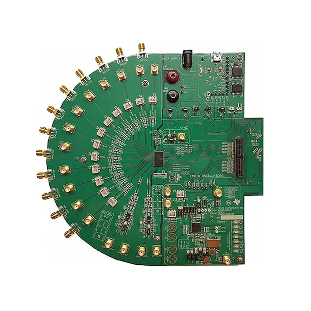


 工商网监
湘ICP备2023018690号
工商网监
湘ICP备2023018690号
