Order
Now
Product
Folder
Support &
Community
Tools &
Software
Technical
Documents
ADS5474
SLAS525D – JULY 2007 – REVISED DECEMBER 2017
ADS5474 14-Bit, 400-MSPS Analog-to-Digital Converter
1 Features
3 Description
•
•
•
•
•
•
•
•
•
•
•
The ADS5474 device is a 14-bit, 400-MSPS analogto-digital converter (ADC) that operates from both a
5-V supply and 3.3-V supply while providing LVDScompatible digital outputs. This ADC is one of a
family of 12-, 13-, and 14-bit ADCs that operate from
210 MSPS to 500 MSPS. The ADS5474 device has
an input buffer that isolates the internal switching of
the onboard track and hold (T&H) from disturbing the
signal source while providing a high-impedance input.
An internal reference generator is also provided to
simplify the system design.
1
•
•
•
•
400-MSPS Sample Rate
14-Bit Resolution, 11.2-Bits ENOB
1.4-GHz Input Bandwidth
80-dBc SFDR at 230 MHz and 400 MSPS
69.8-dBFS SNR at 230 MHz and 400 MSPS
2.2-VPP Differential Input Voltage
LVDS-Compatible Outputs
2.5-W Total Power Dissipation
50-mW Power-Down Mode
Offset Binary Output Format
Output Data Transitions on the Rising and Falling
Edges of a Half-Rate Output Clock
On-Chip Analog Buffer, Track-and-Hold, and
Reference Circuit
HTQFP-80 PowerPAD™ Package
(14-mm × 14-mm Footprint)
Industrial Temperature Range:
–40°C to +85°C
Pin-Similar, -Compatible With 12-, 13-, and 14-Bit
Family: ADS5463, ADS5440, ADS5444
Designed with a 1.4-GHz input bandwidth for the
conversion of wide-bandwidth signals that exceed
400 MHz of input frequency at 400 MSPS, the
ADS5474 device has outstanding low-noise
performance and spurious-free dynamic range over a
large input frequency range.
The ADS5474 device is available in an TQFP-80
PowerPAD package. The device is built on Texas
Instruments complementary bipolar process (BiCom3)
and is specified over the full industrial temperature
range (–40°C to +85°C).
Device Information(1)
PART NUMBER
2 Applications
•
•
•
•
•
•
PACKAGE
ADS5474
Test and Measurement Instrumentation
Software-Defined Radio
Data Acquisition
Power Amplifier Linearization
Communication Instrumentation
Radar
BODY SIZE (NOM)
HTQFP (80)
12.00 mm x 12.00 mm
(1) For all available packages, see the orderable addendum at
the end of the data sheet.
Block Diagram
VIN
VIN
A1
TH1
+
TH2
S
+
TH3
A2
VREF
A3
ADC3
–
–
ADC1
S
DAC1
ADC2
DAC2
Reference
5
5
6
Digital Error Correction
CLK
CLK
Timing
OVR
OVR
DRY
DRY
D[13:0]
1
An IMPORTANT NOTICE at the end of this data sheet addresses availability, warranty, changes, use in safety-critical applications,
intellectual property matters and other important disclaimers. PRODUCTION DATA.
�ADS5474
SLAS525D – JULY 2007 – REVISED DECEMBER 2017
www.ti.com
Table of Contents
1
2
3
4
5
6
Features ..................................................................
Applications ...........................................................
Description .............................................................
Revision History.....................................................
Pin Configuration and Functions .........................
Specifications.........................................................
6.1
6.2
6.3
6.4
6.5
6.6
6.7
7
1
1
1
2
3
6
Absolute Maximum Ratings ..................................... 6
ESD Ratings ............................................................ 6
Recommended Operating Conditions....................... 6
Thermal Information .................................................. 7
Electrical Characteristics........................................... 7
Timing Characteristics............................................. 10
Typical Characteristics ............................................ 12
Detailed Description ............................................ 18
7.1
7.2
7.3
7.4
Overview .................................................................
Functional Block Diagram .......................................
Feature Description.................................................
Device Functional Modes........................................
18
18
18
21
8
Application and Implementation ........................ 24
8.1 Application Information............................................ 24
8.2 Typical Applications ................................................ 24
9
Power Supply Recommendations...................... 28
9.1 Power Supplies ....................................................... 28
10 Layout................................................................... 29
10.1 Layout Guidelines ................................................. 29
10.2 Layout Example .................................................... 30
10.3 Thermal Considerations ........................................ 30
11 Device and Documentation Support ................. 32
11.1
11.2
11.3
11.4
11.5
11.6
11.7
Device Support ....................................................
Documentation Support .......................................
Receiving Notification of Documentation Updates
Community Resources..........................................
Trademarks ...........................................................
Electrostatic Discharge Caution ............................
Glossary ................................................................
32
33
33
33
33
33
34
12 Mechanical, Packaging, and Orderable
Information ........................................................... 34
4 Revision History
Changes from Revision C (January 2016) to Revision D
Page
•
Changed CLK input sample rate (sine wave) parameter maximum specification from 400 MSPS to 404 MSPS ................ 6
•
Changed max sample rate from 400 MHz to 404 MHz in Detailed Design Procedure section ........................................... 25
Changes from Revision B (February 2012) to Revision C
•
Page
Added ESD Ratings table, Feature Description section, Device Functional Modessection, Application and
Implementation section, Power Supply Recommendations section, Layout section, Device and Documentation
Support section, and Mechanical, Packaging, and Orderable Information section ............................................................... 3
Changes from Revision A (August 2008) to Revision B
Page
•
Changed 1.6pF to 2.3pF TYP Input capacitance in ELECTRICAL CHARACTERISTICS ..................................................... 7
•
Changed (where DRY equals the CLK frequency) to (where DRY equals ½ the CLK frequency) in Digital Outputs
section .................................................................................................................................................................................. 21
2
Submit Documentation Feedback
Copyright © 2007–2017, Texas Instruments Incorporated
Product Folder Links: ADS5474
�ADS5474
www.ti.com
SLAS525D – JULY 2007 – REVISED DECEMBER 2017
5 Pin Configuration and Functions
D6
D7
D6
D7
DGND
D8
DVDD3
D9
D8
D10
D9
D11
D10
D12
D11
D13
D12
DRY
D13
DRY
PFP Package
80-Pin HTQFP With PowerPAD
Top View
DVDD3
1
80 79 78 77 76 75 74 73 72 71 70 69 68 67 66 65 64 63 62 61
60
DGND
2
59
D5
58
57
D4
D3
AVDD5
NC
3
4
D5
D4
NC
5
56
VREF
6
55
D3
AGND
54
D2
AVDD5
7
8
53
D2
AGND
9
52
DGND
CLK
10
51
DVDD3
CLK
11
50
D1
ADS5474
AGND
12
49
D1
AVDD5
13
48
D0
AVDD5
14
47
D0
AGND
15
46
NC
AIN
16
45
NC
AIN
17
44
NC
AGND
18
43
NC
AVDD5
19
42
OVR
AGND
20
41
OVR
AGND
AVDD3
AGND
AVDD3
AGND
AGND
AVDD3
PWD
AGND
AGND
AVDD5
VCM
AGND
AGND
AVDD5
AGND
AVDD5
AVDD5
AGND
AVDD5
21 22 23 24 25 26 27 28 29 30 31 32 33 34 35 36 37 38 39 40
P0027-03
(1)
NC - No internal connection.
Submit Documentation Feedback
Copyright © 2007–2017, Texas Instruments Incorporated
Product Folder Links: ADS5474
3
�ADS5474
SLAS525D – JULY 2007 – REVISED DECEMBER 2017
www.ti.com
Pin Functions
PIN
NAME
DESCRIPTION
NO.
TYPE
AIN
16
I
Differential input signal (positive)
AIN
17
I
Differential input signal (negative)
3
8
13
14
19
AVDD5
Analog power supply (5 V)
21
23
25
27
31
35
AVDD3
Analog power supply (3.3 V) (suggestion for ≤ 250 MSPS: leave option to connect to 5 V for
ADS5440, ADS5444 13-bit compatibility)
37
39
1
DVDD3
51
Digital and output driver power supply (3.3 V)
66
7
9
12
15
18
20
22
AGND
24
Analog Ground
26
28
30
32
34
36
38
40
2
DGND
52
Digital Ground
65
CLK
10
I
Differential input clock (positive). Conversion is initiated on rising edge, digital outputs on
falling edge.
CLK
11
I
Differential input clock (negative)
D0
48
D0
47
O
LVDS digital output pair, least significant bit (LSB)
4
Submit Documentation Feedback
Copyright © 2007–2017, Texas Instruments Incorporated
Product Folder Links: ADS5474
�ADS5474
www.ti.com
SLAS525D – JULY 2007 – REVISED DECEMBER 2017
Pin Functions (continued)
PIN
NAME
NO.
D1
50
D1
49
D2
54
D2
53
D3
56
D3
55
D4
58
D4
57
D5
60
D5
59
D6
62
D6
61
D7
64
D7
63
D8
68
D8
67
D9
70
D9
69
D10
72
D10
71
D11
74
D11
73
D12
76
D12
75
D13
78
D13
77
DRY
80
DRY
79
4
5
NC
DESCRIPTION
TYPE
O
LVDS digital output pairs
O
LVDS digital output pair, most significant bit (MSB)
O
Data ready LVDS output pair
-
No connection (pins 4 and 5 should be left floating)
-
No connection (pins 43 to 46 are possible future bit additions for this pinout and therefore can
be connected to a digital bus or left floating)
O
Overrange indicator LVDS output. A logic high signals an analog input in excess of the fullscale range.
O
Common-mode voltage output (3.1 V nominal). Commonly used in DC-coupled applications
to set the input signal to the correct common-mode voltage. A 0.1-μF capacitor from VCM to
AGND is recommended, but not required.
(This pin is not used on the ADS5440, ADS5444, and ADS5463)
43
44
45
46
OVR
42
OVR
41
VCM
29
PWD
33
Power-down (active high). Device is in sleep mode when PWD pin is logic HIGH. ADC
converter is awake when PWD is logic LOW (grounded).
(This pin is not used on the ADS5440, ADS5444, and ADS5463)
VREF
6
Reference voltage input/output (2.4 V nominal). A 0.1-μF capacitor from VREF to AGND is
recommended, but not required.
(Power Pad)
(not
numbered)
Power Pad for thermal relief, also Analog Ground
Submit Documentation Feedback
Copyright © 2007–2017, Texas Instruments Incorporated
Product Folder Links: ADS5474
5
�ADS5474
SLAS525D – JULY 2007 – REVISED DECEMBER 2017
www.ti.com
6 Specifications
6.1 Absolute Maximum Ratings
over operating free-air temperature range, unless otherwise noted. (1)
MIN
MAX
UNIT
AVDD5 to GND
6
Supply voltage AVDD3 to GND
5
DVDD3 to GND
5
Analog input to Valid when supplies are on and within normal ranges. See additional
GND
information in the Power Supplies portion of the applications information
in the back of the datasheet regarding Clock and Analog Inputs when the
Clock input to
supplies are off.
GND
V
–0.3
(AVDD5 + 0.3)
V
–0.3
(AVDD5 + 0.3)
V
CLK to CLK
–2.5
2.5
V
Digital data output to GND
–0.3
(DVDD3 + 0.3)
V
Operating temperature range
–40
85
°C
+150
°C
150
°C
Maximum junction temperature
Storage temperature range
(1)
–65
Stresses beyond those listed under Absolute Maximum Ratings may cause permanent damage to the device. These are stress ratings
only, which do not imply functional operation of the device at these or any other conditions beyond those indicated under Recommended
Operating Conditions. Exposure to absolute-maximum-rated conditions for extended periods may affect device reliability.
6.2 ESD Ratings
V(ESD)
(1)
Electrostatic discharge
Human-body model (HBM), per ANSI/ESDA/JEDEC JS-001
(1)
VALUE
UNIT
2000
V
JEDEC document JEP155 states that 500-V HBM allows safe manufacturing with a standard ESD control process.
6.3 Recommended Operating Conditions
MIN
NOM
MAX
UNIT
SUPPLIES
AVDD5
Analog supply voltage
4.75
5
5.25
V
AVDD3
Analog supply voltage
3.1
3.3
3.6
V
DVDD3
Output driver supply voltage
3
3.3
3.6
V
ANALOG INPUT
VCM
Differential input range
2.2
VPP
Input common mode
3.1
V
10
pF
DIGITAL OUTPUT (DRY, DATA, OVR)
Maximum differential output load
CLOCK INPUT (CLK)
CLK input sample rate (sine wave)
20
404
Clock amplitude, differential sine wave (see Figure 37)
0.5
5
Clock duty cycle (see Figure 31)
TA
6
40%
Operating free-air temperature
–40
Submit Documentation Feedback
50%
MSPS
VPP
60%
+85
°C
Copyright © 2007–2017, Texas Instruments Incorporated
Product Folder Links: ADS5474
�ADS5474
www.ti.com
SLAS525D – JULY 2007 – REVISED DECEMBER 2017
6.4 Thermal Information
ADS5474
THERMAL METRIC (1)
PFP (HTQFP)
UNIT
80 PINS
RθJA
Junction-to-ambient thermal resistance
25.9
°C/W
RθJC(top)
Junction-to-case (top) thermal resistance
7.6
°C/W
RθJB
Junction-to-board thermal resistance
9.8
°C/W
ψJT
Junction-to-top characterization parameter
0.2
°C/W
ψJB
Junction-to-board characterization parameter
9.7
°C/W
RθJC(bot)
Junction-to-case (bottom) thermal resistance
0.2
°C/W
(1)
For more information about traditional and new thermal metrics, see the Semiconductor and IC Package Thermal Metrics application
report.
6.5 Electrical Characteristics
Typical values at TA = 25°C: minimum and maximum values over full temperature range TMIN = –40°C to TMAX = 85°C,
sampling rate = 400 MSPS, 50% clock duty cycle, AVDD5 = 5 V, AVDD3 = 3.3 V, DVDD3 = 3.3 V, –1 dBFS differential input,
and 3-VPP differential clock, unless otherwise noted.
PARAMETER
TEST CONDITIONS
MIN
Resolution
TYP
MAX
UNIT
14
Bits
2.2
VPP
ANALOG INPUTS
Differential input range
Analog input common-mode voltage
Self-biased; see VCM specification below
3.1
V
Input resistance (dc)
Each input to VCM
500
Ω
Input capacitance
Each input to GND
2.3
pF
1.44
GHz
100
dB
2.4
V
Analog input bandwidth (–3dB)
CMRR
Common-mode rejection ratio
Common-mode signal < 50 MHz
(see Figure 27)
INTERNAL REFERENCE VOLTAGE
VREF
VCM
Reference voltage
Analog input common-mode voltage
reference output
With internal VREF. Provided as an output
via the VCM pin for dc-coupled
applications. If an external VREF is used,
the VCM pin tracks as illustrated in
Figure 42
2.9
VCM temperature coefficient
3.1
3.3
–0.8
V
mV/°C
DYNAMIC ACCURACY
No missing codes
Assured
DNL
Differential linearity error
fIN = 70 MHz
INL
Integral linearity error
fIN = 70 MHz
Offset error
–0.99
±0.7
–3
±1
–11
Offset temperature coefficient
1.5
LSB
3
LSB
11
0.02
Gain error
–5
Gain temperature coefficient
mV
mV/°C
5
–0.02
%FS
%FS/°C
POWER SUPPLY
IAVDD5
5-V analog supply current
VIN = full-scale, fIN = 70 MHz,
fS = 400 MSPS
338
372
IAVDD3
3.3-V analog supply current
VIN = full-scale, fIN = 70 MHz,
fS = 400 MSPS
185
201
mA
IDVDD3
3.3-V digital supply current
(includes LVDS)
VIN = full-scale, fIN = 70 MHz,
fS = 400 MSPS
75
83
mA
2.5
2.797
Total power dissipation
Power-up time
From turn-on of AVDD5
50
Submit Documentation Feedback
Copyright © 2007–2017, Texas Instruments Incorporated
Product Folder Links: ADS5474
mA
W
μs
7
�ADS5474
SLAS525D – JULY 2007 – REVISED DECEMBER 2017
www.ti.com
Electrical Characteristics (continued)
Typical values at TA = 25°C: minimum and maximum values over full temperature range TMIN = –40°C to TMAX = 85°C,
sampling rate = 400 MSPS, 50% clock duty cycle, AVDD5 = 5 V, AVDD3 = 3.3 V, DVDD3 = 3.3 V, –1 dBFS differential input,
and 3-VPP differential clock, unless otherwise noted.
PARAMETER
TEST CONDITIONS
MIN
TYP
MAX
UNIT
Wake-up time
From PWD pin switched from HIGH (PWD
active) to LOW (ADC awake)
(see Figure 28)
Power-down power dissipation
PWD pin = logic HIGH
50
PSRR
Power-supply rejection ratio,
AVDD5 supply
Without 0.1-μF board supply capacitors,
with < 1-MHz supply noise (see Figure 46)
75
dB
PSRR
Power-supply rejection ratio,
AVDD3 supply
Without 0.1-μF board supply capacitors,
with < 1-MHz supply noise (see Figure 46)
90
dB
PSRR
Power-supply rejection ratio,
DVDD3 supply
Without 0.1-μF board supply capacitors,
with < 1-MHz supply noise (see Figure 46)
110
dB
5
μs
350
mW
DYNAMIC AC CHARACTERISTICS
fIN = 30 MHz
fIN = 70 MHz
70.3
68.3
fIN = 130 MHz
fIN = 230 MHz
SNR
Signal-to-noise ratio
70.1
68
69.1
fIN = 451 MHz
68.4
fIN = 651 MHz
67.5
fIN = 751 MHz
66.6
fIN = 999 MHz
64.7
fIN = 70 MHz
fIN = 230 MHz
HD2
8
Second-harmonic
86
80
71
80
fIN = 351 MHz
76
fIN = 451 MHz
71
fIN = 651 MHz
60
fIN = 751 MHz
55
fIN = 999 MHz
46
fIN = 30 MHz
89
fIN = 70 MHz
87
fIN = 130 MHz
90
fIN = 230 MHz
84
fIN = 351 MHz
76
fIN = 451 MHz
71
fIN = 651 MHz
74
fIN = 751 MHz
70
fIN = 999 MHz
55
Submit Documentation Feedback
dBFS
88
74
fIN = 130 MHz
Spurious-free dynamic range
69.8
fIN = 351 MHz
fIN = 30 MHz
SFDR
70.2
dBc
dBc
Copyright © 2007–2017, Texas Instruments Incorporated
Product Folder Links: ADS5474
�ADS5474
www.ti.com
SLAS525D – JULY 2007 – REVISED DECEMBER 2017
Electrical Characteristics (continued)
Typical values at TA = 25°C: minimum and maximum values over full temperature range TMIN = –40°C to TMAX = 85°C,
sampling rate = 400 MSPS, 50% clock duty cycle, AVDD5 = 5 V, AVDD3 = 3.3 V, DVDD3 = 3.3 V, –1 dBFS differential input,
and 3-VPP differential clock, unless otherwise noted.
PARAMETER
HD3
Third-harmonic
Worst harmonic, spur
(other than HD2 and HD3)
THD
Total harmonic distortion
TEST CONDITIONS
MIN
93
fIN = 70 MHz
86
fIN = 130 MHz
80
fIN = 230 MHz
80
fIN = 351 MHz
85
fIN = 451 MHz
71
fIN = 651 MHz
60
fIN = 751 MHz
55
fIN = 999 MHz
46
fIN = 30 MHz
95
fIN = 70 MHz
93
fIN = 130 MHz
85
fIN = 230 MHz
85
fIN = 351 MHz
87
fIN = 451 MHz
87
fIN = 651 MHz
90
fIN = 751 MHz
87
fIN = 999 MHz
80
fIN = 30 MHz
86
fIN = 70 MHz
83
fIN = 130 MHz
78
fIN = 230 MHz
77
fIN = 351 MHz
75
fIN = 451 MHz
68
fIN = 651 MHz
60
fIN = 751 MHz
55
fIN = 999 MHz
fIN = 70 MHz
Signal-to-noise and distortion
Two-tone SFDR
ENOB
Effective number of bits
UNIT
dBc
dBc
dBc
69.2
67
fIN = 130 MHz
fIN = 230 MHz
MAX
45
fIN = 30 MHz
SINAD
TYP
fIN = 30 MHz
68.9
68.5
65.5
68.2
fIN = 351 MHz
67.3
fIN = 451 MHz
64.8
fIN = 651 MHz
58.5
fIN = 751 MHz
54
fIN = 999 MHz
45.4
fIN1 = 69 MHz, fIN2 = 70 MHz,
each tone at –7 dBFS
93
fIN1 = 69 MHz, fIN2 = 70 MHz,
each tone at –16 dBFS
95
fIN1 = 297.5 MHz, fIN2 = 302.5 MHz,
each tone at –7 dBFS
85
fIN1 = 297.5 MHz, fIN2 = 302.5 MHz,
each tone at –16 dBFS
83
dBc
dBFS
fIN = 70 MHz
10.8
11.2
fIN = 230 MHz
10.6
10.9
Submit Documentation Feedback
Copyright © 2007–2017, Texas Instruments Incorporated
Product Folder Links: ADS5474
Bits
9
�ADS5474
SLAS525D – JULY 2007 – REVISED DECEMBER 2017
www.ti.com
Electrical Characteristics (continued)
Typical values at TA = 25°C: minimum and maximum values over full temperature range TMIN = –40°C to TMAX = 85°C,
sampling rate = 400 MSPS, 50% clock duty cycle, AVDD5 = 5 V, AVDD3 = 3.3 V, DVDD3 = 3.3 V, –1 dBFS differential input,
and 3-VPP differential clock, unless otherwise noted.
PARAMETER
TEST CONDITIONS
RMS idle-channel noise
MIN
TYP
Inputs tied to common-mode
MAX
1.8
UNIT
LSB
DIGITAL OUTPUTS
VOD
Differential output voltage (±)
VOC
Common-mode output voltage
247
350
454
1.125
1.375
mV
V
DIGITAL INPUTS
VIH
High level input voltage
PWD (pin 33)
VIL
Low level input voltage
PWD (pin 33)
2
0.8
V
V
IIH
High level input current
PWD (pin 33)
1
μA
IIL
Low level input current
PWD (pin 33)
Input capacitance
PWD (pin 33)
–1
μA
2
pF
6.6 Timing Characteristics
Typical values at TA = 25°C: minimum and maximum values over full temperature range TMIN = –40°C to TMAX = 85°C,
sampling rate = 400 MSPS, 50% clock duty cycle, AVDD5 = 5 V, AVDD3 = 3.3 V, DVDD3 = 3.3 V, and 3-VPP differential
clock, unless otherwise noted. (1)
TEST CONDITIONS
ta
MIN
Aperture delay
Aperture jitter, rms
Internal jitter of the ADC
Latency
NOM
MAX
ps
103
fs
3.5
tCLK
Clock period
tCLKH
Clock pulse duration, high
tCLKL
Clock pulse duration, low
2.5
(2)
UNIT
200
cycles
50
ns
1
ns
1
ns
Zero crossing, 10-pF parasitic loading to GND on each
output pin
1000
1400
1800
ps
800
1400
2000
ps
–500
0
500
ps
tDRY
CLK to DRY delay
tDATA
CLK to DATA/OVR delay (2)
Zero crossing, 10-pF parasitic loading to GND on each
output pin
tSKEW
DATA to DRY skew
tDATA – tDRY, 10-pF parasitic loading to GND on each output
pin
tRISE
DRY/DATA/OVR rise time
10-pF parasitic loading to GND on each output pin
500
ps
tFALL
DRY/DATA/OVR fall time
10-pF parasitic loading to GND on each output pin
500
ps
(1)
(2)
10
Timing parameters are ensured by design or characterization, but not production tested.
DRY, DATA, and OVR are updated on the falling edge of CLK. The latency must be added to tDATA to determine the overall propagation
delay.
Submit Documentation Feedback
Copyright © 2007–2017, Texas Instruments Incorporated
Product Folder Links: ADS5474
�ADS5474
www.ti.com
SLAS525D – JULY 2007 – REVISED DECEMBER 2017
Sample
N–1
N+4
N+2
ta
N
N+1
N+3
tCLKH
N+5
tCLKL
CLK
CLK
Latency = 3.5 Clock Cycles
tDRY
DRY
DRY
(1)
tDATA
D[13:0], OVR
N–1
N
N+1
D[13:0], OVR
(1)
Polarity of DRY is undetermined. For further information, see the Digital Outputs section.
Figure 1. Timing Diagram
Submit Documentation Feedback
Copyright © 2007–2017, Texas Instruments Incorporated
Product Folder Links: ADS5474
11
�ADS5474
SLAS525D – JULY 2007 – REVISED DECEMBER 2017
www.ti.com
6.7 Typical Characteristics
At TA = 25°C, sampling rate = 400 MSPS, 50% clock duty cycle, 3-VPP differential sinusoidal clock, analog input amplitude =
–1 dBFS, AVDD5 = 5 V, AVDD3 = 3.3 V, and DVDD3 = 3.3 V, unless otherwise noted.
0
0
SFDR = 88.4 dBc
SNR = 70.3 dBFS
SINAD = 70.2 dBFS
THD = 86 dBc
-20
-20
-40
Amplitude - dB
Amplitude - dB
-40
-60
-60
-80
-80
-100
-100
-120
-120
0
20
40
60
80
100
120
140
160
180
0
200
20
40
60
80
100
120
140
160
180
200
Frequency - MHz
Frequency - MHz
Figure 2. Spectral Performance FFT for 30 MHz Input Signal
Figure 3. Spectral Performance FFT for 70 MHz Input Signal
0
0
SFDR = 78.5 dBc
SNR = 70.1 dBFS
SINAD = 69.5 dBFS
THD = 77.4 dBc
-20
-40
Amplitude - dB
Amplitude - dB
SFDR = 79.7 dBc
SNR = 69.8 dBFS
SINAD = 69.2 dBFS
THD = 76.9 dBc
-20
-40
-60
-60
-80
-80
-100
-100
-120
-120
0
20
40
60
80
100
120 140
160
180
200
0
20
40
60
80
100
120 140
160
180
200
Frequency - MHz
Frequency - MHz
Figure 4. Spectral Performance FFT for 130 MHz Input
Signal
Figure 5. Spectral Performance FFT for 230 MHz Input
Signal
0
0
SFDR = 75.5 dBc
SNR = 69.2 dBFS
SINAD = 68.3 dBFS
THD = 74.7 dBc
-20
-40
Amplitude - dB
Amplitude - dB
SFDR = 71.4 dBc
SNR = 68.4 dBFS
SINAD = 65.8 dBFS
THD = 68.3 dBc
-20
-40
-60
-60
-80
-80
-100
-100
-120
-120
0
12
SFDR = 86.6 dBc
SNR = 70.1 dBFS
SINAD = 69.9 dBFS
THD = 82.9 dBc
20
40
60
80
100
120 140
160
180
200
0
20
40
60
80
100
120 140
160
180
200
Frequency - MHz
Frequency - MHz
Figure 6. Spectral Performance FFT for 351 MHz Input
Signal
Figure 7. Spectral Performance FFT for 451 MHz Input
Signal
Submit Documentation Feedback
Copyright © 2007–2017, Texas Instruments Incorporated
Product Folder Links: ADS5474
�ADS5474
www.ti.com
SLAS525D – JULY 2007 – REVISED DECEMBER 2017
Typical Characteristics (continued)
At TA = 25°C, sampling rate = 400 MSPS, 50% clock duty cycle, 3-VPP differential sinusoidal clock, analog input amplitude =
–1 dBFS, AVDD5 = 5 V, AVDD3 = 3.3 V, and DVDD3 = 3.3 V, unless otherwise noted.
0
0
SFDR = 54.5 dBc
SNR = 66.6 dBFS
SINAD = 55.1 dBFS
THD = 54.4 dBc
-20
-20
-40
Amplitude - dB
-40
Amplitude - dB
SFDR = 46 dBc
SNR = 64.7 dBFS
SINAD = 46.4 dBFS
THD = 45.5 dBc
-60
-60
-80
-80
-100
-100
-120
-120
0
20
40
60
80
100
120 140
160
180
200
0
20
40
60
80
100
120 140
160
180
200
Frequency - MHz
Frequency - MHz
Figure 8. Spectral Performance FFT for 751 MHz Input
Signal
Figure 9. Spectral Performance FFT for 999 MHz Input
Signal
0
0
fIN1 = 69 MHz, -7 dBFS
fIN2 = 70 MHz, -7 dBFS
IMD3 = 97.3 dBFS
SFDR = 93.4 dBFS
-20
-20
-40
Amplitude - dB
-40
Amplitude - dB
fIN1 = 297.5 MHz, -7 dBFS
fIN2 = 302.5 MHz, -7 dBFS
IMD3 = 85.1 dBFS
SFDR = 85 dBFS
-60
-60
-80
-80
-100
-100
-120
-120
0
20
40
60
80
100
120
140
160
180
200
0
20
40
60
80
100
120
140
160
180
200
Frequency - MHz
Frequency - MHz
Figure 10. Two-Tone Intermodulation Distortion (FFT for 69
MHz and 70 MHz at –7 dBFS)
Figure 11. Two-Tone Intermodulation Distortion (FFT for
297.5 MHz and 302.5 MHz at –7 dBFS)
0
0
fIN1 = 69 MHz, -16 dBFS
fIN2 = 70 MHz, -16 dBFS
IMD3 = 98 dBFS
SFDR = 95.7 dFBS
-20
-20
-40
Amplitude - dB
-40
Amplitude - dB
fIN1 = 297.5 MHz, -16 dBFS
fIN2 = 302.5 MHz, -16 dBFS
IMD3 = 94.4 dBFS
SFDR = 83.1 dFBS
-60
-60
-80
-80
-100
-100
-120
-120
0
20
40
60
80
100
120
140
160
180
200
0
Frequency - MHz
20
40
60
80
100
120
140
160
180
200
Frequency - MHz
Figure 12. Two-Tone Intermodulation Distortion (FFT for 69
MHz and 70 MHz at –16 dBFS)
Figure 13. Two-Tone Intermodulation Distortion (FFT for
297.5 MHz and 302.5 MHz at –16 dBFS)
Submit Documentation Feedback
Copyright © 2007–2017, Texas Instruments Incorporated
Product Folder Links: ADS5474
13
�ADS5474
SLAS525D – JULY 2007 – REVISED DECEMBER 2017
www.ti.com
Typical Characteristics (continued)
At TA = 25°C, sampling rate = 400 MSPS, 50% clock duty cycle, 3-VPP differential sinusoidal clock, analog input amplitude =
–1 dBFS, AVDD5 = 5 V, AVDD3 = 3.3 V, and DVDD3 = 3.3 V, unless otherwise noted.
3
0.5
fS = 400 MSPS
fIN = 70 MHz
0.4
0
0.3
-3
Normalized Gain - dB
0.2
-6
0.1
DNL - LSB
-9
0
-0.1
-12
-0.2
-15
-0.3
-18
fS = 400 MSPS
AIN = ±0.38 VPP
-21
10 M
-0.4
-0.5
100 M
1G
5G
0
2048
4096
6144
Frequency - Hz
8192 10240 12288 14336 16384
Code
Figure 14. Normalized Gain Response vs Input Frequency
Figure 15. Differential Nonlinearity
25
2.0
fS = 400 MSPS
fIN = 70 MHz
fS = 400 MSPS
fIN = VCM
1.5
20
Percentage - %
1.0
INL - LSB
0.5
0
15
10
-0.5
5
-1.0
-1.5
8205
8206
8207
8208
8209
8210
8211
8212
8213
8214
8215
8216
8217
8218
8219
8220
8221
8222
8223
8224
8225
8226
8227
0
-2.0
0
2048
4096
6144
8192 10240 12288 14336 16384
Code
Output Code
Figure 16. Integral Nonlinearity
Figure 17. Noise Histogram With Inputs Shorted
120
120
SFDR (dBFS)
SFDR (dBFS)
100
100
SNR (dBFS)
SNR (dBFS)
80
AC Performance - dB
AC Performance - dB
80
60
40
SFDR (dBc)
20
0
60
40
SFDR (dBc)
20
0
SNR (dBc)
SNR (dBc)
-20
-40
-100 -90
14
-20
fS = 400 MSPS
fIN = 70 MHz
-80
-70
-60
-50
-40
-30
-20
-10
fS = 400 MSPS
fIN = 230 MHz
-40
-100 -90
0
-80
-70
-60
-50
-40
-30
-20
-10
0
Input Amplitude - dBFS
Input Amplitude - dBFS
Figure 18. AC Performance vs Input Amplitude (70 MHz
Input Signal)
Figure 19. AC Performance vs Input Amplitude (230 MHz
Input Signal)
Submit Documentation Feedback
Copyright © 2007–2017, Texas Instruments Incorporated
Product Folder Links: ADS5474
�ADS5474
www.ti.com
SLAS525D – JULY 2007 – REVISED DECEMBER 2017
Typical Characteristics (continued)
At TA = 25°C, sampling rate = 400 MSPS, 50% clock duty cycle, 3-VPP differential sinusoidal clock, analog input amplitude =
–1 dBFS, AVDD5 = 5 V, AVDD3 = 3.3 V, and DVDD3 = 3.3 V, unless otherwise noted.
90
100
2f2 - f1 (dBc)
80
2f1 - f2 (dBc)
Performance - dB
70
fS = 400 MSPS
fIN = 230 MHz
88
SFDR - Spurious-Free Dynamic Range - dBc
90
60
50
40
30
20
Worst Spur (dBc)
86
84
+40°C
+65°C
80
78
0°C
76
+85°C
-40°C
+100°C
74
72
10
0
-100 -90
70
-80
-70
-60
-50
-40
-30
-20
4.7
0
-10
4.8
Figure 20. Two-Tone Performance vs Input Amplitude (f1 =
297.5 MHz and f2 = 302.5 MHz)
90
fS = 400 MSPS
fIN = 230 MHz
SFDR - Spurious-Free Dynamic Range - dBc
70.5
+25°C
+40°C
70.0
69.5
-40°C
5.1
5.3
5.2
fS = 400 MSPS
fIN = 230 MHz
88
0°C
5.0
Figure 21. SFDR vs AVDD5 Over Temperature
71.0
+65°C
4.9
AVDD5 - Supply Voltage - V
AIN - dBFS
SNR - Signal-to-Noise Ratio - dBFS
+25°C
82
+85°C
+100°C
69.0
68.5
86
84
+40°C
+25°C
+65°C
82
80
78
+85°C
0°C
76
+100°C
-40°C
74
72
68.0
70
4.7
4.8
4.9
5.0
5.1
3.0
5.3
5.2
3.1
AVDD5 - Supply Voltage - V
Figure 22. SNR vs AVDD5 Over Temperature
71.0
3.4
3.6
3.5
90
fS = 400 MSPS
fIN = 230 MHz
SFDR - Spurious-Free Dynamic Range - dBc
88
70.5
SNR - Signal-to-Noise Ratio - dBFS
3.3
Figure 23. SFDR vs AVDD3 Over Temperature
fS = 400 MSPS
fIN = 230 MHz
+65°C
+40°C
+25°C
70.0
69.5
0°C
3.2
AVDD3 - Supply Voltage - V
+85°C
-40°C
+100°C
69.0
68.5
86
84
+25°C
82
+65°C
+40°C
80
78
76
+85°C
-40°C
0°C
+100°C
74
72
68.0
70
3.0
3.1
3.2
3.3
3.4
3.5
3.6
3.0
3.1
3.2
3.3
3.4
3.5
3.6
AVDD3 - Supply Voltage - V
DVDD3 - Supply Voltage - V
Figure 24. SNR vs AVDD3 Over Temperature
Figure 25. SFDR vs DVDD3 Over Temperature
Submit Documentation Feedback
Copyright © 2007–2017, Texas Instruments Incorporated
Product Folder Links: ADS5474
15
�ADS5474
SLAS525D – JULY 2007 – REVISED DECEMBER 2017
www.ti.com
Typical Characteristics (continued)
At TA = 25°C, sampling rate = 400 MSPS, 50% clock duty cycle, 3-VPP differential sinusoidal clock, analog input amplitude =
–1 dBFS, AVDD5 = 5 V, AVDD3 = 3.3 V, and DVDD3 = 3.3 V, unless otherwise noted.
71.0
0
fS = 400 MSPS
fIN = 230 MHz
CMRR - Common-Mode Rejection Ratio - dB
-10
SNR - Signal-to-Noise Ratio - dBFS
70.5
+25°C
+40°C
0°C
+65°C
70.0
69.5
+85°C
-40°C
+100°C
69.0
68.5
-20
-30
-40
-50
-60
-70
-80
-90
400 MSPS
-100
-110
300 MSPS
-120
68.0
3.0
3.1
3.2
3.3
3.4
-130
100 k
3.6
3.5
1M
10 M
100 M
1G
10 G
DVDD3 - Supply Voltage - V
Frequency - Hz
Figure 26. SNR vs DVDD3 Over Temperature
Figure 27. CMRR vs Common-Mode Input Frequency
75
90
Wake from PDWN
70
SFDR - Spurious-Free Dynamic Range - dBc
65
60
55
SNR - dBFS
50
45
Wake from 5 V Supply
40
35
30
25
20
15
10
85
230 MHz
70 MHz
75
351 MHz
70
65
60
55
fS = 400 MSPS
VCLK = 3 VPP
5
0
10 MHz
80
50
0
10
20
30
40
50
60
70
80
90
100
0
2
1
Time - ms
4
3
5
Clock Common Mode - V
Figure 28. ADC Wakeup Time
Figure 29. SFDR vs Clock Common Mode
90
75
fIN = 10 MHz
fIN = 70 MHz
SFDR - Spurious-Free Dynamic Range - dBc
SNR - Signal-to-Noise Ratio - dBFS
10 MHz
70
70 MHz
351 MHz
65
230 MHz
60
55
fS = 400 MSPS
VCLK = 3 VPP
80
75
fIN = 230 MHz
70
fIN = 300 MHz
65
60
55
fS = 400 MSPS
Clock Input = 3 VPP
50
50
0
16
85
1
2
3
4
5
20
30
40
50
60
70
80
Clock Common Mode - V
Clock Duty Cycle - %
Figure 30. SNR vs Clock Common Mode
Figure 31. SFDR vs Clock Duty Cycle
Submit Documentation Feedback
Copyright © 2007–2017, Texas Instruments Incorporated
Product Folder Links: ADS5474
�ADS5474
www.ti.com
SLAS525D – JULY 2007 – REVISED DECEMBER 2017
Typical Characteristics (continued)
At TA = 25°C, sampling rate = 400 MSPS, 50% clock duty cycle, 3-VPP differential sinusoidal clock, analog input amplitude =
–1 dBFS, AVDD5 = 5 V, AVDD3 = 3.3 V, and DVDD3 = 3.3 V, unless otherwise noted.
400
400
80
68
70
69
85
77
65
73
80
350
350
70
300
70
250
68
69
200
67
70
150
fS - Sampling Frequency - MHz
fS - Sampling Frequency - MHz
77
300
80
85
250
65
73
77
85
70
200
77
80
85
150
68
100
69
70
69
73
100
66
67
68
80
85
85
65
70
77
60
40
40
10
100
200
300
400
500
600
10
100
200
300
56
58
60
62
64
500
600
fIN - Input Frequency - MHz
fIN - Input Frequency - MHz
54
400
66
68
70
50
55
SNR - dBFS
60
65
70
75
80
85
90
SFDR - dBc
Figure 32. SNR vs Input Frequency And Sampling
Frequency
Figure 33. SFDR vs Input Frequency And Sampling
Frequency
Submit Documentation Feedback
Copyright © 2007–2017, Texas Instruments Incorporated
Product Folder Links: ADS5474
17
�ADS5474
SLAS525D – JULY 2007 – REVISED DECEMBER 2017
www.ti.com
7 Detailed Description
7.1 Overview
The ADS5474 device is a 14-bit, 400-MSPS, monolithic pipeline ADC. The bipolar analog core operates from 5-V
and 3.3-V supplies, while the output uses a 3.3-V supply to provide LVDS-compatible outputs. The conversion
process is initiated by the rising edge of the external input clock. At that instant, the differential input signal is
captured by the input track-and-hold (T&H), and the input sample is converted sequentially by a series of lower
resolution stages, with the outputs combined in a digital correction logic block. Both the rising and the falling
clock edges are used to propagate the sample through the pipeline every half clock cycle. This process results in
a data latency of 3.5 clock cycles, after which the output data are available as a 14-bit parallel word, coded in
offset binary format.
7.2 Functional Block Diagram
VIN
VIN
A1
TH1
+
TH2
S
+
TH3
A2
ADC1
A3
ADC3
–
–
VREF
S
DAC1
ADC2
DAC2
Reference
5
5
6
Digital Error Correction
CLK
CLK
Timing
OVR
OVR
DRY
DRY
D[13:0]
7.3 Feature Description
The analog input for the ADS5474 device consists of an analog pseudo-differential buffer followed by a bipolar
transistor T&H. The analog buffer isolates the source driving the input of the ADC from any internal switching and
presents a high impedance that is easy to drive at high input frequencies, compared to an ADC without a
buffered input. The input common-mode is set internally through a 500-Ω resistor connected from 3.1 V to each
of the inputs (common-mode is approximately 2.4 V on 12-bit and 13-bit members of this family). This
configuration results in a differential input impedance of 1 kΩ.
18
Submit Documentation Feedback
Copyright © 2007–2017, Texas Instruments Incorporated
Product Folder Links: ADS5474
�ADS5474
www.ti.com
SLAS525D – JULY 2007 – REVISED DECEMBER 2017
Feature Description (continued)
ADS5463/5474/54RF63
AVDD5
~ 2.5 nH Bond Wire
Buffer
AIN
~ 0.5 pF
Package
~ 200 fF
Bond Pad
500 W
GND
1.6 pF
VCM
AVDD5
1.6 pF
500 W
~ 2.5 nH Bond Wire
GND
AIN
~ 0.5 pF
Package
~ 200 fF
Bond Pad
Buffer
GND
S0293-01
Figure 34. Analog Input Equivalent Circuit
For a full-scale differential input, each of the differential lines of the input signal (pins 16 and 17) swings
symmetrically between (3.1 V + 0.55 V) and (3.1 V – 0.55 V). This range means that each input has a maximum
signal swing of 1.1 VPP for a total differential input signal swing of 2.2 VPP. Operation below 2.2 VPP is allowable,
with the characteristics of performance versus input amplitude demonstrated in Figure 18 and Figure 19. For
instance, for performance at 1.1 VPP rather than 2.2 VPP, refer to the SNR and SFDR at –6 dBFS (0 dBFS =
2.2 VPP). The maximum swing is determined by the internal reference voltage generator, eliminating the need for
any external circuitry for this purpose.
7.3.1 Clock Inputs
The ADS5474 device clock input can be driven with either a differential clock signal or a single-ended clock
input. The characterization of the ADS5474 device is typically performed with a 3-VPP differential clock, but the
ADC performs well with a differential clock amplitude down to approximately 0.5 VPP, as shown in Figure 37. The
clock amplitude becomes more of a factor in performance as the analog input frequency increases. In low-inputfrequency applications, where jitter may not be a big concern, the use of a single-ended clock could save cost
and board space without much performance tradeoff. When clocked with this configuration, it is best to connect
CLK to ground with a 0.01-μF capacitor, while CLK is ac-coupled with a 0.01-μF capacitor to the clock source, as
shown in Figure 36.
Submit Documentation Feedback
Copyright © 2007–2017, Texas Instruments Incorporated
Product Folder Links: ADS5474
19
�ADS5474
SLAS525D – JULY 2007 – REVISED DECEMBER 2017
www.ti.com
Feature Description (continued)
ADS5474
AVDD5
~ 2.5 nH Bond Wire
CLK
~ 200 fF
Bond Pad
~ 0.5 pF
Package
Parasitic
~ 0.2 pF
1000 W
GND
AVDD5
Internal
Clock
Buffer
~ 2.4 V
GND
Parasitic
~ 0.2 pF
1000 W
~ 2.5 nH Bond Wire
CLK
~ 200 fF
Bond Pad
~ 0.5 pF
Package
GND
S0292-04
Figure 35. Clock Input Circuit
90
fS = 400 MSPS
fIN = 230 MHz
85
Square Wave or
Sine Wave
AC Performance - dB
SFDR (dBc)
CLK
0.01 mF
ADS5474
CLK
80
75
70
SNR (dBFS)
0.01 mF
65
60
0
0.5
1.0
1.5
2.0
2.5
3.0
3.5
4.0
4.5
5.0
Clock Amplitude - VPP
Figure 36. Single-Ended Clock
Figure 37. AC Performance vs Clock Level
7.3.2 Digital Outputs
The ADC provides 14 LVDS-compatible, offset binary data outputs (D13 to D0; D13 is the MSB and D0 is the
LSB), a data-ready signal (DRY), and an over-range indicator (OVR). TI recommends using the DRY signal to
capture the output data of the ADS5474 device. DRY is source-synchronous to the DATA/OVR outputs and
operates at the same frequency, creating a half-rate DDR interface that updates data on both the rising and
falling edges of DRY. It is recommended that the capacitive loading on the digital outputs be minimized. Higher
capacitance shortens the data-valid timing window. The values given for timing (see Figure 1) were obtained with
20
Submit Documentation Feedback
Copyright © 2007–2017, Texas Instruments Incorporated
Product Folder Links: ADS5474
�ADS5474
www.ti.com
SLAS525D – JULY 2007 – REVISED DECEMBER 2017
Feature Description (continued)
a measured 10-pF parasitic board capacitance to ground on each LVDS line (or 5-pF differential parasitic
capacitance). When setting the time relationship between DRY and DATA at the receiving device, it is generally
recommended that setup time be maximized, but this partially depends on the setup and hold times of the device
receiving the digital data (like an FPGA or Field Programmable Field Array). Since DRY and DATA are
coincident, it will likely be necessary to delay either DRY or DATA such that setup time is maximized.
Referencing Figure 1, the polarity of DRY with respect to the sample N data output transition is undetermined
because of the unknown startup logic level of the clock divider that generates the DRY signal (DRY is a
frequency divide-by-two of CLK). Either the rising or the falling edge of DRY will be coincident with sample N and
the polarity of DRY could invert when power is cycled off, on or when the power-down pin is cycled. Data capture
from the transition and not the polarity of DRY is recommended, but not required. If the synchronization of
multiple ADS5474 devices is required, it might be necessary to use a form of the CLKIN signal rather than DRY
to capture the data.
The DRY frequency is identical on the ADS5474 and ADS5463 devices (where DRY equals ½ the CLK
frequency), but different on the pin-similar ADS5444 and ADS5440 devices (where DRY equals the CLK
frequency). The LVDS outputs all require an external 100-Ω load between each output pair in order to meet the
expected LVDS voltage levels. For long trace lengths, it may be necessary to place a 100-Ω load on each digital
output as close to the ADS5474 device as possible and another 100-Ω differential load at the end of the LVDS
transmission line to provide matched impedance and avoid signal reflections. The effective load in this case
reduces the LVDS voltage levels by half.
The OVR output equals a logic high when the 14-bit output word attempts to exceed either all 0s or all 1s. This
flag is provided as an indicator that the analog input signal exceeded the full-scale input limit of approximately
2.2 VPP (± gain error). The OVR indicator is provided for systems that use gain control to keep the analog input
signal within acceptable limits.
7.4 Device Functional Modes
7.4.1 External Voltage Reference
For systems that require the analog signal gain to be adjusted or calibrated, this can be performed by using an
external reference. The dependency on the signal amplitude to the value of the external reference voltage is
characterized typically by Figure 38 (VREF = 2.4 V is normalized to 0 dB as this is the internal reference
voltage). As can be seen in the linear fit, this equates to approximately –0.3 dB of signal adjustment per 100 mV
of reference adjustment. The range of allowable variation depends on the analog input amplitude that is applied
to the inputs and the desired spectral performance, as can be seen in the performance versus external reference
graphs in Figure 39 and Figure 40. As the applied analog signal amplitude is reduced, more variation in the
reference voltage is allowed in the positive direction (which equates to a reduction in signal amplitude), whereas
an adjustment in reference voltage below the nominal 2.4 V (which equates to an increase in signal amplitude) is
not recommended below approximately 2.35 V. The power consumption versus reference voltage and operating
temperature should also be considered, especially at high ambient temperatures, because the lifetime of the
device is affected by internal junction temperature (see Figure 48).
Submit Documentation Feedback
Copyright © 2007–2017, Texas Instruments Incorporated
Product Folder Links: ADS5474
21
�ADS5474
SLAS525D – JULY 2007 – REVISED DECEMBER 2017
www.ti.com
Device Functional Modes (continued)
1.0
SFDR - Spurious-Free Dynamic Range - dBc
0.5
Normalized Gain Adjustment - dB
90
fS = 400 MSPS
fIN = 70 MHz
AIN = < -1 dBFS
0
Best Fit:
y = -3.14x + 7.5063
-0.5
-1.0
-1.5
-2.0
AIN = -5 dBFS
80
AIN = -4 dBFS
70
AIN = -3 dBFS
60
AIN = -2 dBFS
AIN = -1 dBFS
50
-2.5
-3.0
2.2
AIN = -6 dBFS
fS = 400 MSPS
fIN = 70 MHz
40
2.3
2.4
2.5
2.6
2.7
2.9
2.8
3.0
2.05 2.15 2.25 2.35 2.45 2.55 2.65 2.75 2.85 2.95 3.05 3.15
3.1
External VREF Applied - V
External VREF Applied - V
Figure 38. Signal Gain Adjustment vs External Reference
(VREF)
Figure 39. SFDR vs External VREF and AIN
75
fS = 400 MSPS
fIN = 70 MHz
AIN = -6 dBFS
SNR - Signal-to-Noise Ratio - V
70
65
60
AIN = -4 dBFS
AIN = -3 dBFS
55
AIN = -2 dBFS
50
AIN = -1 dBFS
AIN = -5 dBFS
45
40
2.05 2.15 2.25 2.35 2.45 2.55 2.65 2.75 2.85 2.95 3.05 3.15
External VREF Applied - V
Figure 40. SNR vs External VREF and AIN
For dc-coupled applications that use the VCM pin of the ADS5474 device as the common mode of the signal in
the analog signal gain path prior to the ADC inputs, the information in Figure 42 is useful to consider versus the
allowable common-mode range of the device that is receiving the VCM voltage, such as an operational amplifier.
Because it is pin-compatible, it is important to note that the ADS5463 does not have a VCM pin and primarily
uses the VREF pin to provide the common-mode voltage in dc-coupled applications. The ADS5463 (VCM =
2.4 V) and ADS5474 (VCM = 3.1 V) devices do not have the same common-mode voltage. To create a board
layout that may accommodate both devices in dc-coupled applications, route VCM and VREF both to a common
point that can be selected via a switch, jumper, or a 0-Ω resistor.
22
Submit Documentation Feedback
Copyright © 2007–2017, Texas Instruments Incorporated
Product Folder Links: ADS5474
�ADS5474
www.ti.com
SLAS525D – JULY 2007 – REVISED DECEMBER 2017
Device Functional Modes (continued)
3.4
3.8
fS = 400 MSPS
fIN = 70 MHz
fS = 400 MSPS
fIN = 70 MHz
3.7
3.2
VCM Pin Output Voltage - V
3.6
Power - W
3.0
2.8
2.6
2.4
3.5
3.4
3.3
3.2
3.1
3.0
2.2
2.9
2.0
2.8
2.05 2.15 2.25 2.35 2.45 2.55 2.65 2.75 2.85 2.95 3.05 3.15
2.05 2.15 2.25 2.35 2.45 2.55 2.65 2.75 2.85 2.95 3.05 3.15
External VREF Applied - V
External VREF Applied - V
Figure 41. Total Power Consumption vs External VREF
Figure 42. VCM Pin Output vs External VREF
Submit Documentation Feedback
Copyright © 2007–2017, Texas Instruments Incorporated
Product Folder Links: ADS5474
23
�ADS5474
SLAS525D – JULY 2007 – REVISED DECEMBER 2017
www.ti.com
8 Application and Implementation
NOTE
Information in the following applications sections is not part of the TI component
specification, and TI does not warrant its accuracy or completeness. TI’s customers are
responsible for determining suitability of components for their purposes. Customers should
validate and test their design implementation to confirm system functionality.
8.1 Application Information
In the design of any application involving a high-speed data converter, particular attention should be paid to the
design of the analog input, the clocking solution, and careful layout of the clock and analog signals. The
ADS5474 evaluation module (EVM) is one practical example of the design of the analog input circuit and clocking
solution, as well as a practical example of good circuit board layout practices around the ADC.
8.2 Typical Applications
The analog inputs of the ADS5474 must be fully differential and biased to an appropriate common mode voltage,
VCM. It is rare that the end equipment will have a signal that already meets the requisite amplitude and common
mode and is fully differential. Therefore, there will be a signal conditioning circuit for the analog input. If the
amplitude of the input circuit is such that no gain is needed to make full use of the full-scale range of the ADC,
then a transformer coupled circuit as used on the EVM may be used with good results. The transformer coupling
is inherently low-noise, and inherently AC-coupled so that the signal may be biased to VCM after the transformer
coupling.
If signal gain is required, or the input bandwidth is to include the spectrum all the way down to DC such that AC
coupling is not possible, then an amplifier-based signal conditioning circuit would be required. Figure 43 shows
LMH3401 interfaced with ADS5474. LMH3401 is configured to have to Single-Ended input with a differential
outputs follow by 1st Nyquist based low pass filter with 375-MHz bandwidth. Power supply recommendations for
the amplifier are also shown in the figure below.
200
5.3 pF
LMH3401
10
40
26 nH
VIN(50 Ohm)
2.6 pF
12.5
50
10
12.5
40
5.3 pF
+
2.5 V
–
ADS5474
26 nH
VCM
200
VCM = 2.5 V
0.01 µF
Amp Supply Voltage:
Vs+ = 5 V
Vs- = 0 V
Figure 43. Application Diagram
Clocking a High Speed ADC such as the ADS5474 requires a fully differential clock signal from a clean, low-jitter
clock source and driven by an appropriate clock buffer, often with LVPECL or LVDS signaling levels. The sample
clock is internally biased to the desired level if the sample clock is AC coupled to the ADS5474. Figure 44 shows
the typical AC coupling and termination circuit used for an AC coupled clock source.
24
Submit Documentation Feedback
Copyright © 2007–2017, Texas Instruments Incorporated
Product Folder Links: ADS5474
�ADS5474
www.ti.com
SLAS525D – JULY 2007 – REVISED DECEMBER 2017
Typical Applications (continued)
0.1 µF
CLKINP
RT
Clock Buffer
0.1 µF
RT
CLKINN
0.1 µF
Figure 44. Recommended Differential Clock Driving Circuit
8.2.1 Design Requirements
The ADS5474 requires a fully differential analog input with a full-scale range not to exceed 2.2-V peak to peak
differential, biased to a common mode voltage of 3.1 V. In addition the input circuit must provide proper
transmission line termination (or proper load resistors in an amplifier-based solution) so the input of the
impedance of the ADC analog inputs should be considered as well.
The ADS5474 is capable of a typical SNR of 70.1 dBFS for input frequencies of about 130 MHz, which is well
under the Nyquist limit for this ADC operating at 400 Msps. The amplifier and clocking solution will have a direct
impact on performance in terms of SNR, so the amplifier and clocking solution should be selected such that the
SNR performance of at least 69 dBFS is preserved.
8.2.2 Detailed Design Procedure
The ADS5474 has a max sample rate of 404 MHz and an input bandwidth of approximately 1440 MHz, but an
application involving the first Nyquist zone is being considered, therefore limit the frequency bandwidth here to be
under 200 MHz.
8.2.2.1 Clocking Source for ADC5474
The signal to noise ratio of the ADC is limited by three different factors: the quantization noise, the thermal noise,
and the total jitter of the sample clock. Quantization noise is driven by the resolution of the ADC, which is 14 bits
for the ADS5474. Thermal noise is typically not noticeable in high speed pipelined converters such as the
ADS5474, but may be estimated by looking at the signal to noise ratio of the ADC with very low input frequencies
and using Equation 1 to solve for thermal noise. (For this estimation, we will look to the ADS5474 datasheet and
take the specified SNR for the lowest frequency listed. The lowest input frequency listed for the ADS5474 is at 30
MHz, and the SNR at that frequency is 70.3 dB, so we will use 70.3 dB as our SNR limit due to thermal noise.
This is just an approximation, and the lower the input frequency that has an SNR specification the better this
approximation would be.) The thermal noise limits the SNR at low input frequencies while the clock jitter sets the
SNR for higher input frequencies.
Quantization noise is also a limiting factor for SNR, as the theoretical maximum achievable SNR as a function of
the number of bits of resolution is set by Equation 1.
SNRMAX = 1.76 + (6.02 ´ N )
where
•
N = number of bits resolution
(1)
For a 14-bit ADC, the maximum SNR = 1.76 + (6.02 × 14) = 86.04 dB. This is the number that we shall enter into
Equation 2 for quantization noise as we solve for total SNR for different amounts of clock jitter using Equation 2.
SNRADC[dBc] = -20 ´ log (10 - SNRQuantization _ Noise ) 2 + (10 20
SNRThermalNoise 2
SNRJitter 2
) + (10 )
20
20
(2)
The SNR limitation due to sample clock jitter can be calculated using Equation 3:
SNRJitter[dBc] = -20 ´ log(2p ´ fIN ´ tJitter )
(3)
Submit Documentation Feedback
Copyright © 2007–2017, Texas Instruments Incorporated
Product Folder Links: ADS5474
25
�ADS5474
SLAS525D – JULY 2007 – REVISED DECEMBER 2017
www.ti.com
Typical Applications (continued)
The clock jitter in Equation 3 is the total amount of clock jitter, whether the jitter source is internal to the ADC
itself or external due to the clocking source. The total clock jitter (tJitter) has two components – the internal
aperture jitter (103 fs for ADS5474) which is set by the noise of the clock input buffer, and the external clock jitter
from the clocking source and all associated buffering of the clock signal. Total clock jitter can be calculated from
the aperture jitter and the external clock jitter as in Equation 4.
TJitter = (TJitter , Ext .CLock _ Input ) 2 + (TAperture _ ADC ) 2
(4)
External clock jitter can be minimized by using high quality clock sources and jitter cleaners as well as bandpass
filters at the clock input while a faster clock slew rate may at times also improve the ADC aperture jitter slightly.
The ADS5474 has an internal aperture jitter of 103 fs, which is largely fixed. The SNR depending on the amount
of external jitter for different input frequencies is shown in Figure 45. Often the design requirements will list a
target SNR for a system, and Equation 1 through Equation 3 are then used to calculate the external clock jitter
needed from the clocking solution to meet the system objectives.
Figure 45 shows that with an external clock jitter of 100 fs rms, the expected SNR of the ADS5474 would be
greater than 69 dBFS at an input tone of 200 MHz, which is the Nyquist limit. Having less external clock jitter
such as 35 fs rms or even 50 fs rms would result in an SNR that would exceed our design target, but at possibly
the expense of a more costly clocking solution. Having external clock jitter of 150 fs rms or more would fail to
meet the design target.
8.2.2.2 Amplifier Selection
The amplifier and any input filtering will have its own SNR performance, and the SNR performance of the
amplifier front end will combine with the SNR of the ADC itself to yield a system SNR that is less than that of the
ADC itself. System SNR can be calculated from the SNR of the amplifier conditioning circuit and the overall ADC
SNR as in Equation 5. In Equation 5, the SNR of the ADC would be the value derived from the datasheet
specifications and the clocking derivation presented in the previous section.
SNRSystem = -20 ´ log (10
- SNRADC
20
) 2 + (10
- SNRAMP + Filter
20
)2
(5)
The signal-to-noise ratio (SNR) of the amplifier and filter can be calculated from the noise specifications in the
datasheet for the amplifier, the amplitude of the signal, and the bandwidth of the filter. The noise from the
amplifier is band-limited by the filter and the rolloff of the filter will depend on the order of the filter, therefore the
user should replace the filter rolloff with an equivalent brick-wall filter bandwidth. For example, a first order filter
may be approximated by a brick-wall filter with bandwidth of 1.57 times the bandwidth of the first order filter. We
will assume a first order filter for this design. The amplifier and filter noise can be calculated using Equation 6:
26
Submit Documentation Feedback
Copyright © 2007–2017, Texas Instruments Incorporated
Product Folder Links: ADS5474
�ADS5474
www.ti.com
SLAS525D – JULY 2007 – REVISED DECEMBER 2017
Typical Applications (continued)
SNRAMP + Filter = 10 ´ log(
VO 2
E
) = 20 ´ log(
2
FILTEROUT
VO
EFILTEROUT
)
where
•
•
•
•
EFILTEROUT = ENAMPOUT × √ENB
ENAMPOUT = the output noise density of the LMH3401 (3.4 nV / √Hz)
ENB = the brick-wall equivalent noise bandwidth of the filter
VO = the amplifier output signal. (which will be full scale input of the ADC expressed in rms)
(6)
In Equation 6, the parameters of the equation can be seen to be in terms of signal amplitude in the numerator
and amplifier noise in the denominator, or SNR. For the numerator, use the full scale voltage specification of the
ADS5474, or 2.2 V peal to peak differential. Because Equation 6 requires the signal voltage to be in rms, convert
2.2 V p-p to 0.7766 V rms.
The noise specification for the LMH3401 is listed as 3.4 (nV/√Hz), so we will use this value to integrate the noise
component from DC out to the filter cutoff, using the equivalent brick wall filter of 200 MHz × 1.57, or 314 MHz.
3.4 (nV/√Hz) × 314 MHz yields 60248 nV, or 60.25 µV.
Using 0.7766 V rms for VO and 60.25 µV for Efilterout, the SNR of the amplifier and filter as given by Equation 6 is
approximately 82.2 dB.
Taking the SNR of the ADC as 69.2 dB from Figure 45, and SNR of the amplifier and filter as 82.2 dB,
Equation 5 predicts the system SNR to be 68.99 dB. In other words, the SNR of the ADC and the SNR of the
front end combine as the square root of the sum of squares, and since the SNR of the amplifier front end is seen
to be much greater than the SNR of the ADC in this example, the SNR of the ADC dominates Equation 5 and the
system SNR is seen to be nearly the SNR of the ADC itself. We assumed our design requirement to be 69 dB,
and after a clocking solution was chosen and an amplifier, filter solution was chosen we have a predicted SNR of
68.99 dB. If we deem 68.99 dB to not be close enough, or wish to have some margin in the design, then either
improving the clock jitter from 100 fs to 50 fs, or replacing the first order filter with a second order filter would get
the predicted system SNR above the 69-dB design requirement.
8.2.3 Application Curves
Figure 45 shows the SNR of the ADC as a function of clock jitter and input frequency for the ADS5474. This plot
of curves take into account the aperture jitter of the ADC, the number of bits of resolution, and the thermal noise
estimation so that the figure may be used to predict SNR for a given input frequency and external clock jitter.
This figure then may be used to set the jitter requirement for the clocking solution for a given input bandwidth
and given design goal for SNR.
75
35 fs
50 fs
100 fs
150 fs
200 fs
73
71
SNR (dBFS)
69
67
65
63
61
59
57
55
10
20 30
50 70 100
200 300 500
Fin (MHz)
1000 2000
5000
D001
Figure 45. SNR vs Input Frequency and External Clock Jitter
Submit Documentation Feedback
Copyright © 2007–2017, Texas Instruments Incorporated
Product Folder Links: ADS5474
27
�ADS5474
SLAS525D – JULY 2007 – REVISED DECEMBER 2017
www.ti.com
9 Power Supply Recommendations
9.1 Power Supplies
The ADS5474 device uses three power supplies. For the analog portion of the design, a 5-V and 3.3-V supply
(AVDD5 and AVDD3) are used, while the digital portion uses a 3.3-V supply (DVDD3). Using low-noise power
supplies with adequate decoupling is recommended. Linear supplies are preferred to switched supplies, as
switched supplies tend to generate more noise components that can be coupled to the ADS5474 device.
However, the PSRR value and the plot shown in Figure 46 were obtained without bulk supply decoupling
capacitors. When bulk (0.1-μF) decoupling capacitors are used, the board-level PSRR is much higher than the
stated value for the ADC. The user may be able to supply power to the device with a less-than-ideal supply and
still achieve good performance. It is not possible to make a single recommendation for every type of supply and
level of decoupling for all systems. If the noise characteristics of the available supplies are understood, a study of
the PSRR data for the ADS5474 device may provide the user with enough information to select noisy supplies if
the performance is still acceptable within the frequency range of interest. The power consumption of the
ADS5474 device does not change substantially over clock rate or input frequency as a result of the architecture
and process. The DVDD3 PSRR is superior to both the AVDD5 and AVDD3, and therefore was not graphed.
Because there are two diodes connected in reverse between AVDD3 and DVDD3 internally, a power-up
sequence is recommended. When there is a delay in power up between these two supplies, the one that lags
could have current sinking through an internal diode before it powers up. The sink current can be large or small
depending on the impedance of the external supply and could damage the device or affect the supply source.
The best power up sequence is one of the following options (regardless of when AVDD5 powers up):
1) Power up both AVDD3 and DVDD3 at the same time (best scenario), OR
2) Keep the voltage difference less than 0.8 V between AVDD3 and DVDD3 during the power up (0.8 V is not a
hard specification - a smaller delta between supplies is safer).
If the above sequences are not practical then the sink current from the supply must be controlled or protection
added externally. The max transient current (on the order of μsec) for DVDD3 or AVDD3 pin is 500 mA to avoid
potential damage to the device or reduce its lifetime.
Values for analog and clock input given in the Absolute Maximum Ratings are valid when the supplies are on.
When the power supplies are off and the clock or analog inputs are still alive, the input voltage and current must
be limited to avoid device damage. If the ADC supplies are off, the max, min continuous DC voltage is ±0.95 V
and max DC current is 20 mA for each input pin (clock or analog), relative to ground.
0
fS = 400 MSPS
PSRR - Power-Supply Rejection Ratio - dB
-10
-20
-30
-40
AVDD5
-50
-60
-70
-80
AVDD3
-90
-100
-110
DVDD3
-120
100 k
1M
10 M
100 M
1G
Frequency - Hz
Figure 46. PSRR vs Supply Injected Frequency
28
Submit Documentation Feedback
Copyright © 2007–2017, Texas Instruments Incorporated
Product Folder Links: ADS5474
�ADS5474
www.ti.com
SLAS525D – JULY 2007 – REVISED DECEMBER 2017
10 Layout
10.1 Layout Guidelines
The evaluation board represents a good model of how to lay out the printed circuit board (PCB) to obtain the
maximum performance from the ADS5474 device. Follow general design rules such as the use of multilayer
boards, a single ground plane for ADC ground connections, and local decoupling ceramic chip capacitors. The
analog input traces should be isolated from any external source of interference or noise, including the digital
outputs as well as the clock traces. The clock signal traces should also be isolated from other signals, especially
in applications such as high IF sampling where low jitter is required. Besides performance-oriented rules, care
must be taken when considering the heat dissipation of the device. The thermal heatsink included on the bottom
of the package should be soldered to the board as described in the PowerPad Package section. See the
ADS5474 EVM User Guide (SLAU194) on the TI web site for the evaluation board schematic.
10.1.1 PowerPAD Package
The PowerPAD package is a thermally-enhanced, standard-size IC package designed to eliminate the use of
bulky heatsinks and slugs traditionally used in thermal packages. This package can be easily mounted using
standard PCB assembly techniques, and can be removed and replaced using standard repair procedures.
The PowerPAD package is designed so that the leadframe die pad (or thermal pad) is exposed on the bottom of
the IC. This pad design provides an extremely low thermal resistance path between the die and the exterior of
the package. The thermal pad on the bottom of the IC can then be soldered directly to the PCB, using the PCB
as a heatsink.
10.1.1.1 Assembly Process
1. Prepare the PCB top-side etch pattern including etch for the leads as well as the thermal pad as illustrated in
the Mechanical Data section (at the end of this data sheet).
2. Place a 6 × 6 array of thermal vias in the thermal pad area. These holes should be 13 mils (0.013 in or
0.3302 mm) in diameter. The small size prevents wicking of the solder through the holes.
3. It is recommended to place a small number of 25-mil (0.025-in or 0.635-mm) diameter holes under the
package, but outside the thermal pad area, to provide an additional heat path.
4. Connect all holes (both those inside and outside the thermal pad area) to an internal copper plane (such as a
ground plane).
5. Do not use the typical web or spoke via-connection pattern when connecting the thermal vias to the ground
plane. The spoke pattern increases the thermal resistance to the ground plane.
6. The top-side solder mask should leave exposed the terminals of the package and the thermal pad area.
7. Cover the entire bottom side of the PowerPAD vias to prevent solder wicking.
8. Apply solder paste to the exposed thermal pad area and all of the package terminals.
For more detailed information regarding the PowerPAD package and its thermal properties, see either the
PowerPAD Made Easy application brief (SLMA004) or the PowerPAD Thermally Enhanced Package application
report (SLMA002), both available for download at www.ti.com.
Submit Documentation Feedback
Copyright © 2007–2017, Texas Instruments Incorporated
Product Folder Links: ADS5474
29
�ADS5474
SLAS525D – JULY 2007 – REVISED DECEMBER 2017
www.ti.com
10.2 Layout Example
Clock Input
Analog Input
LVDS Data Output
*Solid Black is top layer ground fill
Figure 47. ADS5474 Board Layout
10.3 Thermal Considerations
It is important for applications that anticipate running continuously for long periods of time near the maximumrated ambient temperature of 85°C to consider the data shown in Figure 48. Referring to the Thermal Information
table, the worst-case operating condition with no airflow has a thermal rise of 23.7°C/W. At approximately 2.5 W
of normal power dissipation, at a maximum ambient of 85°C with no airflow, the junction temperature of the
ADS5474 device reaches approximately 85°C + (23.7°C/W × 2.5 W) = +144°C. Being even more conservative
and accounting for the maximum possible power dissipation that is ensured (2.797 W), the junction temperature
becomes nearly 150°C. As Figure 48 shows, this performance limits the expected lifetime of the ADS5474
device. Operation at 85°C continuously can require airflow or an additional heatsink in order to decrease the
internal junction temperature and increase the expected lifetime (because of electromigration failures). An airflow
of 250 LFM (linear feet per minute) reduces the thermal resistance to 16.4°C/W and, therefore, the maximum
junction temperature to 131°C, assuming a worst-case of 2.797 W and 85°C ambient.
The ADS5474 device performance over temperature is quite good and can be seen starting in Figure 21. Though
the typical plots show good performance at 100°C, the device is only rated from –40°C to 85°C. For continuous
operation at temperatures near or above the maximum, the expected primary negative effect is a shorter device
lifetime because of the electromigration failures at high junction temperatures. The maximum recommended
continuous junction temperature is 150°C.
30
Submit Documentation Feedback
Copyright © 2007–2017, Texas Instruments Incorporated
Product Folder Links: ADS5474
�ADS5474
www.ti.com
SLAS525D – JULY 2007 – REVISED DECEMBER 2017
Thermal Considerations (continued)
Estimated Life - Years
1000
100
10
1
80
90
100
110
120
130
140
150
160
170
180
Continuous Junction Temperature - °C
Figure 48. Operating Life Derating Chart, Electromigration Fail Mode
Submit Documentation Feedback
Copyright © 2007–2017, Texas Instruments Incorporated
Product Folder Links: ADS5474
31
�ADS5474
SLAS525D – JULY 2007 – REVISED DECEMBER 2017
www.ti.com
11 Device and Documentation Support
11.1 Device Support
11.1.1 Device Nomenclature
Analog Bandwidth The analog input frequency at which the power of the fundamental is reduced by 3 dB with
respect to the low-frequency value.
Aperture Delay The delay in time between the rising edge of the input sampling clock and the actual time at
which the sampling occurs.
Aperture Uncertainty (Jitter) The sample-to-sample variation in aperture delay.
Clock Pulse Duration/Duty Cycle The duty cycle of a clock signal is the ratio of the time the clock signal
remains at a logic high (clock pulse duration) to the period of the clock signal, expressed as a
percentage.
Differential Nonlinearity (DNL) An ideal ADC exhibits code transitions at analog input values spaced exactly 1
LSB apart. DNL is the deviation of any single step from this ideal value, measured in units of LSB.
Common-Mode Rejection Ratio (CMRR) CMRR measures the ability to reject signals that are presented to
both analog inputs simultaneously. The injected common-mode frequency level is translated into
dBFS, the spur in the output FFT is measured in dBFS, and the difference is the CMRR in dB.
Effective Number of Bits (ENOB) ENOB is a measure in units of bits of converter performance as compared to
the theoretical limit based on quantization noise:
ENOB = (SINAD – 1.76)/6.02
Gain Error
(7)
Gain error is the deviation of the ADC actual input full-scale range from its ideal value, given as a
percentage of the ideal input full-scale range.
Integral Nonlinearity (INL) INL is the deviation of the ADC transfer function from a best-fit line determined by a
least-squares curve fit of that transfer function. The INL at each analog input value is the difference
between the actual transfer function and this best-fit line, measured in units of LSB.
Offset Error Offset error is the deviation of output code from mid-code when both inputs are tied to commonmode.
Power-Supply Rejection Ratio (PSRR) PSRR is a measure of the ability to reject frequencies present on the
power supply. The injected frequency level is translated into dBFS, the spur in the output FFT is
measured in dBFS, and the difference is the PSRR in dB. The measurement calibrates out the
benefit of the board supply decoupling capacitors.
Signal-to-Noise Ratio (SNR) SNR is the ratio of the power of the fundamental (PS) to the noise floor power
(PN), excluding the power at dc and in the first five harmonics. SNR is either given in units of dBc
(dB to carrier) when the absolute power of the fundamental is used as the reference, or dBFS (dB
to full-scale) when the power of the fundamental is extrapolated to the converter full-scale range.
P
SNR + 10log 10 S
PN
(8)
Signal-to-Noise and Distortion (SINAD) SINAD is the ratio of the power of the fundamental (PS) to the power
of all the other spectral components including noise (PN) and distortion (PD), but excluding dc.
SINAD is either given in units of dBc (dB to carrier) when the absolute power of the fundamental is
used as the reference, or dBFS (dB to full-scale) when the power of the fundamental is
extrapolated to the converter full-scale range.
PS
SINAD + 10log 10
PN ) PD
(9)
Temperature Drift Temperature drift (with respect to gain error and offset error) specifies the change from the
value at the nominal temperature to the value at TMIN or TMAX. It is computed as the maximum
variation the parameters over the whole temperature range divided by TMIN – TMAX.
Total Harmonic Distortion (THD) THD is the ratio of the power of the fundamental (PS) to the power of the first
32
Submit Documentation Feedback
Copyright © 2007–2017, Texas Instruments Incorporated
Product Folder Links: ADS5474
�ADS5474
www.ti.com
SLAS525D – JULY 2007 – REVISED DECEMBER 2017
Device Support (continued)
five harmonics (PD).THD is typically given in units of dBc (dB to carrier).
P
THD + 10log 10 S
PD
(10)
Two-Tone Intermodulation Distortion (IMD3) IMD3 is the ratio of the power of the fundamental (at frequencies
f1, f2) to the power of the worst spectral component at either frequency 2f1 – f2 or 2f2 – f1). IMD3 is
given in units of either dBc (dB to carrier) when the absolute power of the fundamental is used as
the reference, or dBFS (dB to full-scale) when the power of the fundamental is extrapolated to the
converter full-scale range.
11.2 Documentation Support
11.2.1 Related Documentation
For related documentation see the following:
• Clocking High Speed Data Converters
• PowerPAD Thermally Enhanced Package
• PowerPAD Made Easy
• ADS5474 EVM User Guide
• ADS5463 12-bit, 500 MSPS Analog-to-Digital Converter with Buffered Input
• ADS5440 13-Bit 210 MSPS Analog-to-Digital Converter
• ADS5444 13-Bit 250 MSPS Analog-to-Digital Converter
• LMK04808 IBIS Model
• LMH3401 7-GHz, Ultra-Wideband, Fixed-Gain, Fully-Differential Amplifier
11.3 Receiving Notification of Documentation Updates
To receive notification of documentation updates, navigate to the device product folder on ti.com. In the upper
right corner, click on Alert me to register and receive a weekly digest of any product information that has
changed. For change details, review the revision history included in any revised document.
11.4 Community Resources
The following links connect to TI community resources. Linked contents are provided "AS IS" by the respective
contributors. They do not constitute TI specifications and do not necessarily reflect TI's views; see TI's Terms of
Use.
TI E2E™ Online Community TI's Engineer-to-Engineer (E2E) Community. Created to foster collaboration
among engineers. At e2e.ti.com, you can ask questions, share knowledge, explore ideas and help
solve problems with fellow engineers.
Design Support TI's Design Support Quickly find helpful E2E forums along with design support tools and
contact information for technical support.
11.5 Trademarks
PowerPAD, E2E are trademarks of Texas Instruments.
All other trademarks are the property of their respective owners.
11.6 Electrostatic Discharge Caution
This integrated circuit can be damaged by ESD. Texas Instruments recommends that all integrated circuits be handled with
appropriate precautions. Failure to observe proper handling and installation procedures can cause damage.
ESD damage can range from subtle performance degradation to complete device failure. Precision integrated circuits may be more
susceptible to damage because very small parametric changes could cause the device not to meet its published specifications.
Submit Documentation Feedback
Copyright © 2007–2017, Texas Instruments Incorporated
Product Folder Links: ADS5474
33
�ADS5474
SLAS525D – JULY 2007 – REVISED DECEMBER 2017
www.ti.com
11.7 Glossary
SLYZ022 — TI Glossary.
This glossary lists and explains terms, acronyms, and definitions.
12 Mechanical, Packaging, and Orderable Information
The following pages include mechanical, packaging, and orderable information. This information is the most
current data available for the designated devices. This data is subject to change without notice and revision of
this document. For browser-based versions of this data sheet, refer to the left-hand navigation.
34
Submit Documentation Feedback
Copyright © 2007–2017, Texas Instruments Incorporated
Product Folder Links: ADS5474
�PACKAGE OPTION ADDENDUM
www.ti.com
10-Dec-2020
PACKAGING INFORMATION
Orderable Device
Status
(1)
Package Type Package Pins Package
Drawing
Qty
Eco Plan
(2)
Lead finish/
Ball material
MSL Peak Temp
Op Temp (°C)
Device Marking
(3)
(4/5)
(6)
ADS5474IPFP
ACTIVE
HTQFP
PFP
80
96
RoHS & Green
NIPDAU
Level-4-260C-72 HR
-40 to 85
ADS5474I
ADS5474IPFPR
ACTIVE
HTQFP
PFP
80
1000
RoHS & Green
NIPDAU
Level-4-260C-72 HR
-40 to 85
ADS5474I
ADS5474IPFPRG4
ACTIVE
HTQFP
PFP
80
1000
RoHS & Green
NIPDAU
Level-4-260C-72 HR
-40 to 85
ADS5474I
(1)
The marketing status values are defined as follows:
ACTIVE: Product device recommended for new designs.
LIFEBUY: TI has announced that the device will be discontinued, and a lifetime-buy period is in effect.
NRND: Not recommended for new designs. Device is in production to support existing customers, but TI does not recommend using this part in a new design.
PREVIEW: Device has been announced but is not in production. Samples may or may not be available.
OBSOLETE: TI has discontinued the production of the device.
(2)
RoHS: TI defines "RoHS" to mean semiconductor products that are compliant with the current EU RoHS requirements for all 10 RoHS substances, including the requirement that RoHS substance
do not exceed 0.1% by weight in homogeneous materials. Where designed to be soldered at high temperatures, "RoHS" products are suitable for use in specified lead-free processes. TI may
reference these types of products as "Pb-Free".
RoHS Exempt: TI defines "RoHS Exempt" to mean products that contain lead but are compliant with EU RoHS pursuant to a specific EU RoHS exemption.
Green: TI defines "Green" to mean the content of Chlorine (Cl) and Bromine (Br) based flame retardants meet JS709B low halogen requirements of
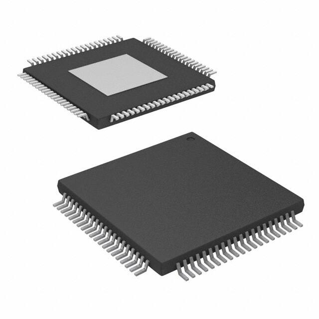


 工商网监
湘ICP备2023018690号
工商网监
湘ICP备2023018690号
