Product
Folder
Sample &
Buy
Support &
Community
Tools &
Software
Technical
Documents
Reference
Design
ADS5560, ADS5562
SLWS207B – MAY 2008 – REVISED JANUARY 2016
ADS556x 16-Bit, 40 and 80 MSPS ADCs With DDR LVDS and CMOS Outputs
•
•
•
•
•
The device is specified over the
temperature range of –40°C to 85°C.
Device Information(1)
PART NUMBER
ADS5560
Medical Imaging, MRI
Wireless Communications Infrastructure
Software Defined Radio
Test and Measurement Instrumentation
High Definition Video
PACKAGE
BODY SIZE (NOM)
VQFN (48)
ADS5562
7.00 mm × 7.00 mm
(1) For all available packages, see the orderable addendum at
the end of the data sheet.
Block Diagram
2 Applications
•
•
•
•
•
industrial
CLKP
CLKOUTP
CLOCKGEN
CLKM
DRGND
•
•
•
•
•
The device can be put in an external reference mode,
where the VCM pin behaves as the external
reference input. For applications where power is
important, the ADS556x device offers power down
modes and automatic power scaling at lower sample
rates.
DRVDD
•
16-Bit Resolution
Maximum Sample Rate:
– ADS5562: 80 MSPS
– ADS5560: 40 MSPS
Total Power:
– 865 mW at 80 MSPS
– 674 mW at 40 MSPS
No Missing Codes
High SNR: 84 dBFS (3 MHz IF)
SFDR: 85 dBc (3 MHz IF)
Low-Frequency Noise Suppression Mode
Programmable Fine Gain, 1-dB steps Until 6-dB
Maximum Gain
Double Data-Rate (DDR) LVDS and Parallel
CMOS Output Options
Internal and External Reference Support
3.3-V Analog and Digital Supply
Pin-for-Pin With ADS5547 Family
48-VQFN Package (7.00 mm × 7.00 mm)
AGND
•
•
1
Innovative techniques, such as DDR LVDS and an
internal reference that does not require external
decoupling capacitors, have been used to achieve
significant savings in pin count. This innovation
results in a compact 7-mm × 7-mm 48-pin VQFN
package.
AVDD
1 Features
CLKOUTM
D0_D1_P
D0_D1_M
D2_D3_P
D2_D3_M
D4_D5_P
INP
INM
Sample
and
Hold
Digital
Encoder
and
Serializer
16-Bit ADC
D4_D5_M
D6_D7_P
D6_D7_M
3 Description
D8_D9_M
D10_D11_P
VCM
Control
Interface
Reference
D10_D11_M
D12_D13_P
D12_D13_M
D14_D15_P
D14_D15_M
OVR
OE
DFS
MODE
SEN
SDATA
ADS556x
RESET
In addition to high performance, the device offers
several flexible features such as output interface
(either Double Data Rate [DDR] LVDS or parallel
CMOS) and fine gain in 1-dB steps until 6-dB
maximum gain.
D8_D9_P
SCLK
The ADS556x is a high-performance 16-bit family of
ADCs with sampling rates up to 80 MSPS. The
device supports very-high SNR for input frequencies
in the first Nyquist zone. The device includes a lowfrequency noise suppression mode that improves the
noise from DC to about 1 MHz.
LVDS INTERFACE
B0095-05
1
An IMPORTANT NOTICE at the end of this data sheet addresses availability, warranty, changes, use in safety-critical applications,
intellectual property matters and other important disclaimers. PRODUCTION DATA.
�ADS5560, ADS5562
SLWS207B – MAY 2008 – REVISED JANUARY 2016
www.ti.com
Table of Contents
1
2
3
4
5
6
Features ..................................................................
Applications ...........................................................
Description .............................................................
Revision History.....................................................
Pin Configuration and Functions .........................
Specifications.........................................................
6.1
6.2
6.3
6.4
6.5
6.6
1
1
1
2
4
8
Absolute Maximum Ratings ...................................... 8
ESD Ratings.............................................................. 8
Recommended Operating Conditions....................... 9
Thermal Information .................................................. 9
Electrical Characteristics......................................... 10
AC Electrical Characteristics for ADS5560 Fs = 40
MSPS ....................................................................... 11
6.7 AC Electrical Characteristics for ADS5562, Fs = 80
MSPS ....................................................................... 12
6.8 Electrical Characteristics for ADS5562 ................... 13
6.9 Electrical Characteristics for ADS5560 ................... 13
6.10 Digital Characteristics ........................................... 14
6.11 Timing Characteristics for LVDS and CMOS Modes
................................................................................. 14
6.12 Serial Interface Timing Characteristics ................. 15
6.13 Reset Timing ......................................................... 15
6.14 Timing Characteristics at Lower Sampling
Frequencies ............................................................. 16
6.15 Typical Characteristics .......................................... 19
7
Detailed Description ............................................ 25
7.1
7.2
7.3
7.4
7.5
7.6
8
Overview .................................................................
Functional Block Diagram ......................................
Feature Description.................................................
Device Functional Modes........................................
Programming...........................................................
Register Maps .........................................................
25
25
26
29
35
39
Application and Implementation ........................ 45
8.1 Application Information............................................ 45
8.2 Typical Application ................................................. 45
9 Power Supply Recommendations...................... 49
10 Layout................................................................... 49
10.1 Layout Guidelines ................................................. 49
10.2 Layout Example ................................................... 50
11 Device and Documentation Support ................. 51
11.1
11.2
11.3
11.4
11.5
11.6
11.7
Device Support......................................................
Documentation Support ........................................
Related Links ........................................................
Community Resources..........................................
Trademarks ...........................................................
Electrostatic Discharge Caution ............................
Glossary ................................................................
51
52
52
53
53
53
53
12 Mechanical, Packaging, and Orderable
Information ........................................................... 53
4 Revision History
NOTE: Page numbers for previous revisions may differ from page numbers in the current version.
Changes from Revision A (May 2012) to Revision B
•
Page
Added ESD Ratings table, Feature Description section, Device Functional Modes, Application and Implementation
section, Power Supply Recommendations section, Layout section, Device and Documentation Support section, and
Mechanical, Packaging, and Orderable Information section. ................................................................................................. 1
Changes from Original (May 2008) to Revision A
Page
•
Changed Programmable Fine Gain in FEATURES................................................................................................................ 1
•
Added maximum gain to end of second paragraph of DESCRIPTION.................................................................................. 1
•
Changed Voltage between AVDD to DRVDD to Voltage between AVDD and DRVDD in ABS MAX RATINGS .................. 8
•
Added Voltage applied to analog input pins, INP, INM in ABS MAX RATINGS .................................................................... 8
•
Added Voltage applied to analog input pins, CLKP, CLKM, MODE in ABS MAX RATINGS ................................................ 8
•
Added Voltage applied to analog input pins, RESET, SCLK, SDATA, SEN, OE, DFS in ABS MAX RATINGS ................... 8
•
Changed boundary between DEFAULT SPEED mode and LOW SPEED mode from 30 MSPS to 25 MSPS in
RECOMMENDED OPERATING CONDITIONS .................................................................................................................... 9
•
Changed tho to th in header row of Timing Characteristics at Lower Sampling Frequencies ............................................... 16
•
Added text to Note regarding RESET pulse requirement in Figure 1 .................................................................................. 16
•
Added 32k Point FFT to TYPICAL CHARACTERISTICS section conditions ...................................................................... 19
•
Changed Figure 48............................................................................................................................................................... 28
•
Added text to end of Programmable Fine Gain section ....................................................................................................... 29
•
Added (Serial Interface Mode) to Table 1 title...................................................................................................................... 29
•
Changed LOW SPEED mode boundary from 30 MSPS to 25 MSPS in Low Sampling Frequency Operation section ...... 29
2
Submit Documentation Feedback
Copyright © 2008–2016, Texas Instruments Incorporated
Product Folder Links: ADS5560 ADS5562
�ADS5560, ADS5562
www.ti.com
SLWS207B – MAY 2008 – REVISED JANUARY 2016
•
Added text to Clock Input section......................................................................................................................................... 30
•
Changed Clock Input section paragraphs and 4 illustrations ............................................................................................... 30
•
Added (of width greater than 10ns) in USING SERIAL INTERFACE PROGRAMMING ONLY section .............................. 36
•
Added to Priority last row in Table 3 ................................................................................................................................... 36
•
Changed Parallel Interface Control description for SCLK Control Pin, (SCLK = 0, 3dB gain; SCLK = DRVDD, 1 dB
gain) in Table 4..................................................................................................................................................................... 37
•
Changed first pargraph in SERIAL INTERFACE section ..................................................................................................... 38
•
Added text to Table 9 Note................................................................................................................................................... 39
•
Changed Fs > 30 MSPS to Fs > 25 MSPS in .......................................................................................... 41
Copyright © 2008–2016, Texas Instruments Incorporated
Product Folder Links: ADS5560 ADS5562
Submit Documentation Feedback
3
�ADS5560, ADS5562
SLWS207B – MAY 2008 – REVISED JANUARY 2016
www.ti.com
5 Pin Configuration and Functions
37 D4_D5_M
38 D4_D5_P
39 D6_D7_M
40 D6_D7_P
41 D8_D9_M
42 D8_D9_P
43 D10_D11_M
44 D10_D11_P
45 D12_D13_M
46 D12_D13_P
47 D14_D15_M
48 D14_D15_P
RGZ Package
48-Pin VQFN With Exposed Thermal Pad
LVDS Mode – Top View
DRGND
1
36 DRGND
DRVDD
2
35 DRVDD
OVR
3
34 D2_D3_P
CLKOUTM
4
33 D2_D3_M
CLKOUTP
5
32 D0_D1_P
DFS
6
31 D0_D1_M
Thermal Pad
OE
7
30 RESET
AVDD
8
29 SCLK
AGND
9
28 SDATA
AVDD 24
MODE 23
AVDD 22
NC 21
AVDD 20
AGND 19
AVDD 18
AGND 17
25 AGND
INM 16
26 AVDD
INP 15
CLKM 11
AGND 12
AGND 14
27 SEN
VCM 13
CLKP 10
Pin Functions - LVDS Mode
PIN
I/O
DESCRIPTION
NO.
NAME
9, 12, 14,
17, 19,
25
AGND
I
Analog ground
8, 18, 20,
22, 24,
26
AVDD
I
Analog power supply
4
CLKOUTM
O
Differential output clock, complement
5
CLKOUTP
O
Differential output clock, true
10
CLKP
11
CLKM
I
Differential clock input
31
D0_D1_M
O
Differential output data D0 and D1 multiplexed, complement.
32
D0_D1_P
O
Differential output data D0 and D1 multiplexed, true
43
D10_D11_M
O
Differential output data D10 and D11 multiplexed, complement
44
D10_D11_P
O
Differential output data D10 and D11 multiplexed, true
45
D12_D13_M
O
Differential output data D12 and D13 multiplexed, complement
46
D12_D13_P
O
Differential output data D12 and D13 multiplexed, true
47
D14_D15_M
O
Differential output data D14 and D15 multiplexed, complement
48
D14_D15_P
O
Differential output data D14 and D15 multiplexed, true
33
D2_D3_M
O
Differential output data D2 and D3 multiplexed, complement
34
D2_D3_P
O
Differential output data D2 and D3 multiplexed, true
37
D4_D5_M
O
Differential output data D4 and D5 multiplexed, complement
38
D4_D5_P
O
Differential output data D4 and D5 multiplexed, true
4
Submit Documentation Feedback
Copyright © 2008–2016, Texas Instruments Incorporated
Product Folder Links: ADS5560 ADS5562
�ADS5560, ADS5562
www.ti.com
SLWS207B – MAY 2008 – REVISED JANUARY 2016
Pin Functions - LVDS Mode (continued)
PIN
NO.
NAME
I/O
DESCRIPTION
39
D6_D7_M
O
Differential output data D6 and D7 multiplexed, complement
40
D6_D7_P
O
Differential output data D6 and D7 multiplexed, true
41
D8_D9_M
O
Differential output data D8 and D9 multiplexed, complement
42
D8_D9_P
O
Differential output data D8 and D9 multiplexed, true
6
DFS
I
Data Format Select input.
This pin sets the DATA FORMAT (2s complement or Offset binary) and the LVDS/CMOS output
mode type. See Table 7 for detailed information.
The pin has an internal 100-kΩ pulldown resistor to DRGND.
1, 36
DRGND
I
Digital and output buffer ground
2, 35
DRVDD
I
Digital and output buffer supply
I
Differential analog input
Mode select input.
This pin selects the Internal or External reference mode. See Table 8 for detailed information.
The pin has an internal 100-kΩ pulldown resistor to AGND.
15
INP
16
INM
23
MODE
I
21
NC
—
7
OE
I
Output buffer enable input, active high.
The pin has an internal 100-kΩ pullup resistor to DRVDD.
3
OVR
O
Out-of-range indicator, CMOS level signal
Do not connect
30
RESET
I
Serial interface reset input.
When using the serial interface, the user should apply a high-going pulse on this pin to reset the
internal registers.
When the serial interface is not used, the user should tie RESET permanently high. (SCLK,
SDATA and SEN can be used as parallel pin controls).
The pin has an internal 100-kΩ pulldown resistor to DRGND.
29
SCLK
I
This pin functions as serial interface clock input when RESET is low.
It functions as LOW SPEED MODE control when RESET is tied high. See Table 4 for detailed
information.
The pin has an internal 100-kΩ pulldown resistor to DRGND.
28
SDATA
I
This pin functions as serial interface data input when RESET is low.
It functions as STANDBY control pin when RESET is tied high.
See Table 5 for detailed information.
The pin has an internal 100-kΩ pulldown resistor to DRGND.
27
SEN
I
This pin functions as serial interface enable input when RESET is low.
It functions as CLKOUT edge programmability when RESET is tied high. See Table 6 for detailed
information.
The pin has an internal 100-kΩ pullup resistor to DRVDD.
13
VCM
I/O
Internal reference mode – Common-mode voltage output.
External reference mode – Reference input. The voltage forced on this pin sets the internal
reference.
—
PAD
—
Connect the PAD to the ground plane. See the Exposed Thermal Pad section.
Copyright © 2008–2016, Texas Instruments Incorporated
Product Folder Links: ADS5560 ADS5562
Submit Documentation Feedback
5
�ADS5560, ADS5562
SLWS207B – MAY 2008 – REVISED JANUARY 2016
www.ti.com
37 D4
38 D5
39 D6
40 D7
41 D8
42 D9
43 D10
44 D11
45 D12
46 D13
47 D14
48 D15
RGZ Package
48-Pin VQFN With Exposed Thermal Pad
CMOS Mode – Top View
DRGND
1
36 DRGND
DRVDD
2
35 DRVDD
OVR
3
34 D3
UNUSED
4
33 D2
CLKOUT
5
32 D1
DFS
6
OE
7
30 RESET
AVDD
8
29 SCLK
AGND
9
28 SDATA
31 D0
Thermal Pad
AVDD 24
MODE 23
AVDD 22
NC 21
AVDD 20
AGND 19
AVDD 18
AGND 17
25 AGND
INP 15
AGND 12
INM 16
26 AVDD
VCM 13
27 SEN
AGND 14
CLKP 10
CLKM 11
Pin Functions - CMOS Mode
PIN
I/O
DESCRIPTION
NO.
NAME
9, 12, 14,
17, 19,
25
AGND
I
Analog ground
8, 18, 20,
22, 24,
26
AVDD
I
Analog power supply
5
CLKOUT
O
CMOS output clock
10
CLKP
11
CLKM
I
Differential clock input
31
D0
O
CMOS output data D0
32
D1
O
CMOS output data D1
43
D10
O
CMOS output data D10
44
D11
O
CMOS output data D11
45
D12
O
CMOS output data D12
46
D13
O
CMOS output data D13
47
D14
O
CMOS output data D14
48
D15
O
CMOS output data D15
33
D2
O
CMOS output data D2
34
D3
O
CMOS output data D3
37
D4
O
CMOS output data D4
38
D5
O
CMOS output data D5
39
D6
O
CMOS output data D6
40
D7
O
CMOS output data D7
41
D8
O
CMOS output data D8
42
D9
O
CMOS output data D9
6
Submit Documentation Feedback
Copyright © 2008–2016, Texas Instruments Incorporated
Product Folder Links: ADS5560 ADS5562
�ADS5560, ADS5562
www.ti.com
SLWS207B – MAY 2008 – REVISED JANUARY 2016
Pin Functions - CMOS Mode (continued)
PIN
NO.
NAME
I/O
DESCRIPTION
DFS
I
Data Format Select input.
This pin sets the DATA FORMAT (2s complement or Offset binary) and the LVDS/CMOS output
mode type. See Table 7 for detailed information.
The pin has an internal 100-kΩ pulldown resistor to DRGND.
1, 36
DRGND
I
Digital and output buffer ground
2, 35
DRVDD
I
Digital and output buffer supply
I
Differential analog input
Mode select input.
This pin selects the Internal or External reference mode. See Table 8 for detailed information.
The pin has an internal 100-kΩ pulldown resistor to AGND.
6
15
INP
16
INM
23
MODE
I
21
NC
—
7
OE
I
Output buffer enable input, active high.
The pin has an internal 100-kΩ pullup resistor to DRVDD.
3
OVR
O
Out-of-range indicator, CMOS level signal
Do not connect
30
RESET
I
Serial interface reset input.
When using the serial interface, the user should apply a high-going pulse on this pin to reset the
internal registers.
When the serial interface is not used, the user should tie RESET permanently high. (SCLK,
SDATA and SEN can be used as parallel pin controls).
The pin has an internal 100-kΩ pulldown resistor to DRGND.
29
SCLK
I
This pin functions as serial interface clock input when RESET is low.
It functions as LOW SPEED MODE control when RESET is tied high. See Table 4 for detailed
information.
The pin has an internal 100-kΩ pulldown resistor to DRGND.
28
SDATA
I
This pin functions as serial interface data input when RESET is low.
It functions as STANDBY control pin when RESET is tied high.
See Table 5 for detailed information.
The pin has an internal 100-kΩ pulldown resistor to DRGND.
27
SEN
I
This pin functions as serial interface enable input when RESET is low.
It functions as CLKOUT edge programmability when RESET is tied high. See Table 6 for detailed
information.
The pin has an internal 100-kΩ pullup resistor to DRVDD.
4
UNUSED
—
Unused pin in CMOS mode
13
VCM
I/O
Internal reference mode – Common-mode voltage output.
External reference mode – Reference input. The voltage forced on this pin sets the internal
references.
—
PAD
—
Connect the PAD to the ground plane. See the Exposed Thermal Pad section.
Copyright © 2008–2016, Texas Instruments Incorporated
Product Folder Links: ADS5560 ADS5562
Submit Documentation Feedback
7
�ADS5560, ADS5562
SLWS207B – MAY 2008 – REVISED JANUARY 2016
www.ti.com
6 Specifications
6.1 Absolute Maximum Ratings
over operating free-air temperature range (unless otherwise noted) (1)
Supply voltage
MIN
MAX
UNIT
AVDD
–0.3
3.9
V
DRVDD
–0.3
3.9
V
Voltage between AGND and DRGND
–0.3
0.3
V
Voltage between AVDD and DRVDD
–0.3
3.3
V
Voltage applied to VCM pin (in external reference mode)
V
Voltage applied to
analog input pins
–0.3
1.8
INP, INM
–0.3
(3.6, AVDD + 0.3 )
CLKP, CLKM (2), MODE
–0.3
(3.6, AVDD + 0.3 )
RESET, SCLK, SDATA, SEN, OE, DFS
–0.3
(3.6, DRVDD + 0.3 )
V
–40
85
°C
V
TA
Operating free-air temperature
Tjmax
Operating junction temperature
125
°C
Lead temperature 1,6 mm (1/16") from the case for 10 s
220
°C
150
°C
TSTG
(1)
(2)
Storage temperature
–65
Stresses beyond those listed under Absolute Maximum Ratings may cause permanent damage to the device. These are stress ratings
only, which do not imply functional operation of the device at these or any other conditions beyond those indicated under Recommended
Operating Conditions. Exposure to absolute-maximum-rated conditions for extended periods may affect device reliability.
When AVDD is turned off, TI recommends switching off the input clock (or ensure the voltage on CLKP, CLKM is 25
80
MSPS
1
25
MSPS
> 25
40
MSPS
1
25
MSPS
0.4
VPP
45%
50%
55%
DIGITAL OUTPUTS
CL
Maximum external load capacitance from each output pin to DRGND (LVDS and CMOS
modes)
RL
Differential external load resistance between the LVDS output pairs (LVDS mode)
Operating free-air temperature
(1)
(2)
5
pF
Ω
100
–40
85
°C
See the Low Sampling Frequency Operation section for details.
Supported clock waveform formats: sine wave, LVPECL, LVDS, and LVCMOS
6.4 Thermal Information
THERMAL METRIC (1)
ADS5560
ADS5562
RGZ (VQFN)
UNIT
48 PINS
RθJA
Junction-to-ambient thermal resistance
27.6
°C/W
RθJC(top)
Junction-to-case (top) thermal resistance
12.4
°C/W
RθJB
Junction-to-board thermal resistance
4.4
°C/W
ψJT
Junction-to-top characterization parameter
0.2
°C/W
ψJB
Junction-to-board characterization parameter
4.4
°C/W
RθJC(bot)
Junction-to-case (bottom) thermal resistance
0.9
°C/W
(1)
For more information about traditional and new thermal metrics, see the Semiconductor and IC Package Thermal Metrics application
report, SPRA953.
Copyright © 2008–2016, Texas Instruments Incorporated
Product Folder Links: ADS5560 ADS5562
Submit Documentation Feedback
9
�ADS5560, ADS5562
SLWS207B – MAY 2008 – REVISED JANUARY 2016
www.ti.com
6.5 Electrical Characteristics
Typical values are at 25°C, AVDD = DRVDD = 3.3 V, sampling rate = Maximum Rated, sine wave input clock, 1.5-VPP clock
amplitude, 50% clock duty cycle, –1-dBFS differential analog input, internal reference mode, DDR LVDS interface, default fine
gain (1 dB). Minimum and maximum values are across the full temperature range TMIN = –40°C to TMAX = 85°C, AVDD =
DRVDD = 3.3 V, sampling rate = Maximum Rated, unless otherwise noted.
PARAMETER
TEST CONDITIONS
MIN
Resolution
TYP
MAX
UNIT
16
bits
3.56
VPP
ANALOG INPUT
Differential input voltage range
(1)
Differential input capacitance
VCM
5
pF
Analog input bandwidth
300
MHz
Analog input common-mode current
(per input pin)
6.6
μA/MSPS
Common-mode output voltage
Internal reference mode
1.5
V
VCM output current capability
Internal reference mode
±4
mA
DC ACCURACY
No Missing Codes
DNL
Differential non-linearity
INL
0-dB gain
Assured
–0.95
0.5
3
LSB
Integral non-linearity
–8.5
±3
8.5
LSB
Offset error
–25
±10
25
Offset error temperature coefficient
Variation of offset error across AVDD
supply
mV
0.005
mV/°C
1.5
mV/V
There are two sources of gain error: I) internal reference inaccuracy and ii) channel gain error
EGREF
Gain error due to internal reference
inaccuracy alone
–2.5
±1
2.5
% full scale
ECHAN
Channel gain error alone
–2.5
±1
2.5
% full scale
Channel gain error temperature
coefficient
Δ%/°C
0.01
POWER SUPPLY
IAVDD
IDRVDD
Analog supply current
Digital supply current
ADS5560
210
250
ADS5562
160
190
LVDS mode
CL = 5 pF, IO = 3.5 mA, RL =
100 Ω
ADS5560
52
ADS5562
44
CMOS mode
CL = 5 pF, FIN = 3 MHz
ADS5560
60
ADS5562
37
ADS5560
865
1100
ADS5562
674
810
ADS5560
155
ADS5562
135
Total power
LVDS mode
Standby power
STANDBY mode with clock
running
Clock stop power
(1)
10
125
mA
mA
mA
mW
mW
150
mW
The full-scale voltage range is a function of the fine gain settings. See Table 1.
Submit Documentation Feedback
Copyright © 2008–2016, Texas Instruments Incorporated
Product Folder Links: ADS5560 ADS5562
�ADS5560, ADS5562
www.ti.com
SLWS207B – MAY 2008 – REVISED JANUARY 2016
6.6 AC Electrical Characteristics for ADS5560 Fs = 40 MSPS
Typical values are at 25°C, AVDD = DRVDD = 3.3 V, sampling rate = Maximum Rated, sine wave input clock, 1.5-VPP clock
amplitude, 50% clock duty cycle, –1-dBFS differential analog input, internal reference mode, DDR LVDS interface, 0 dB fine
gain (1). Minimum and maximum values are across the full temperature range TMIN = –40°C to TMAX = 85°C, AVDD = DRVDD
= 3.3 V, sampling rate = Maximum Rated, default fine gain (1 dB), unless otherwise noted.
PARAMETER
TEST CONDITIONS
MIN
FIN = 3 MHz
LVDS interface
SNR
Signal to noise ratio
82.5
FIN = 30 MHz
81.8
81.8
FIN = 30 MHz
81.6
1.42
FIN = 3 MHz
SINAD
Signal to noise and distortion
ratio
ENOB
Effective number of bits
76
79
FIN = 30 MHz
77
79.3
FIN = 30 MHz
78
12.4
(1)
LSB
dBFS
dBFS
13.5
bits
90
FIN = 10 MHz
78
88
FIN = 25 MHz
83
FIN = 30 MHz
79
FIN = 3 MHz
HD2
Second harmonic
81.4
FIN = 25 MHz
LVDS interface, FIN = 10 MHz
dBFS
82
75
FIN = 3 MHz
SFDR
Spurious free dynamic range
83
FIN = 25 MHz
FIN = 10 MHz
dBFS
83.2
FIN = 3 MHz
CMOS interface
83.1
FIN = 25 MHz
FIN = 10 MHz
UNIT
83.5
78
Inputs tied to common-mode
LVDS interface
84
FIN = 25 MHz
FIN = 10 MHz
MAX
84.3
80
FIN = 3 MHz
CMOS interface
RMS output noise
FIN = 10 MHz
TYP
dBc
94
FIN = 10 MHz
78
92
FIN = 25 MHz
90
FIN = 30 MHz
88
dBc
After reset, the device is initialized to 1-dB fine gain setting. For SFDR and SNR performance across fine gains, see the Typical
Characteristics section.
Copyright © 2008–2016, Texas Instruments Incorporated
Product Folder Links: ADS5560 ADS5562
Submit Documentation Feedback
11
�ADS5560, ADS5562
SLWS207B – MAY 2008 – REVISED JANUARY 2016
www.ti.com
6.7 AC Electrical Characteristics for ADS5562, Fs = 80 MSPS
Typical values are at 25°C, AVDD = DRVDD = 3.3 V, sampling rate = Maximum Rated, sine wave input clock, 1.5-VPP clock
amplitude, 50% clock duty cycle, –1-dBFS differential analog input, internal reference mode, DDR LVDS interface, 0 dB fine
gain (1). Minimum and maximum values are across the full temperature range TMIN = –40°C to TMAX = 85°C, AVDD = DRVDD
= 3.3 V, sampling rate = Maximum Rated, default fine gain (1 dB), unless otherwise noted.
PARAMETER
TEST CONDITIONS
MIN
TYP
79
83.8
FIN = 3 MHz
LVDS interface
SNR
Signal to noise ratio
RMS output noise
FIN = 25 MHz
83.2
FIN = 30 MHz
82.8
77
80.7
FIN = 30 MHz
80.4
1.42
ENOB
Effective number of bits
FIN = 10 MHz
75
79.5
FIN = 30 MHz
79
(1)
12
LSB
dBFS
80.5
FIN = 10 MHz
73.5
80.2
FIN = 25 MHz
79.3
FIN = 30 MHz
77.9
LVDS interface, FIN = 10 MHz
12.2
dBFS
13.1
bits
85
FIN = 10 MHz
77
85
FIN = 25 MHz
83
FIN = 30 MHz
80
FIN = 3 MHz
HD2
Second harmonic
80.5
FIN = 25 MHz
FIN = 3 MHz
SFDR
Spurious free dynamic range
dBFS
80.5
FIN = 3 MHz
CMOS interface
81.4
FIN = 25 MHz
FIN = 3 MHz
SINAD
Signal to noise and distortion
ratio
dBFS
81.7
FIN = 10 MHz
Inputs tied to common-mode
LVDS interface
UNIT
84
FIN = 10 MHz
FIN = 3 MHz
CMOS interface
MAX
dBc
90
FIN = 10 MHz
77
89
FIN = 25 MHz
88
FIN = 30 MHz
88
dBc
After reset, the device is initialized to 1-dB fine gain setting. For SFDR and SNR performance across fine gains, see the Typical
Characteristics section.
Submit Documentation Feedback
Copyright © 2008–2016, Texas Instruments Incorporated
Product Folder Links: ADS5560 ADS5562
�ADS5560, ADS5562
www.ti.com
SLWS207B – MAY 2008 – REVISED JANUARY 2016
6.8 Electrical Characteristics for ADS5562
Typical values are at 25°C, AVDD = DRVDD = 3.3 V, sampling rate = Maximum Rated, sine wave input clock, 1.5-VPP clock
amplitude, 50% clock duty cycle, –1-dBFS differential analog input, 0 dB fine gain (1), internal reference mode, DDR LVDS
interface. Minimum and maximum values are across the full temperature range TMIN = –40°C to TMAX = 85°C, AVDD =
DRVDD = 3.3 V, sampling rate = Maximum Rated, default fine gain (1 dB), unless otherwise noted.
PARAMETER
TEST CONDITIONS
MIN
TYP
FIN = 3 MHz
HD3
Third harmonic
Worst harmonic
other than HD2, HD3
UNIT
85
FIN = 10 MHz
77
85
FIN = 25 MHz
dBc
83
FIN = 30 MHz
80
FIN = 3 MHz
104
FIN = 10 MHz
102
FIN = 25 MHz
100
FIN = 30 MHz
100
FIN = 3 MHz
THD
Total harmonic distortion
MAX
dBc
84
FIN = 10 MHz
75.5
83
FIN = 25 MHz
82
dBc
FIN = 30 MHz
80
IMD
Two-tone intermodulation
distortion
FIN1 = 5 MHz, FIN2 = 10 MHz, each tone –7 dBFS
92
dBFS
Voltage overload recovery time
Recovery to 1% for 6-dB overload
1
clock
cycles
(1)
After reset, the device is initialized to 1-dB fine gain setting. For SFDR and SNR performance across fine gains, see the Typical
Characteristics section.
6.9 Electrical Characteristics for ADS5560
Typical values are at 25°C, AVDD = DRVDD = 3.3 V, sampling rate = Maximum Rated, sine wave input clock, 1.5-VPP clock
amplitude, 50% clock duty cycle, –1-dBFS differential analog input, internal reference mode, DDR LVDS interface, 0 dB fine
gain (1). Minimum and maximum values are across the full temperature range TMIN = –40°C to TMAX = 85°C, AVDD = DRVDD
= 3.3 V, sampling rate = Maximum Rated, default fine gain (1 dB), unless otherwise noted.
PARAMETER
TEST CONDITIONS
MIN
FIN = 3 MHz
HD3
Third harmonic
Worst harmonic
other than HD2, HD3
THD
Total harmonic distortion
TYP
MAX
UNIT
90
FIN = 10 MHz
78
FIN = 25 MHz
88
FIN = 30 MHz
79
FIN = 3 MHz
104
FIN = 10 MHz
102
FIN = 25 MHz
101
FIN = 30 MHz
101
FIN = 3 MHz
88
FIN = 10 MHz
dBc
83
76.5
dBc
86
dBc
FIN = 25 MHz
81
FIN = 30 MHz
78
IMD
Two-tone intermodulation
distortion
FIN1 = 5 MHz, FIN2 = 10 MHz, each tone –7 dBFS
98
dBFS
Voltage overload recovery time
Recovery to 1% for 6-dB overload
1
clock
cycles
(1)
After reset, the device is initialized to 1-dB fine gain setting. For SFDR and SNR performance across fine gains, see the Typical
Characteristics section.
Copyright © 2008–2016, Texas Instruments Incorporated
Product Folder Links: ADS5560 ADS5562
Submit Documentation Feedback
13
�ADS5560, ADS5562
SLWS207B – MAY 2008 – REVISED JANUARY 2016
www.ti.com
6.10 Digital Characteristics
DC specifications refer to the condition where the digital outputs are not switching, but are permanently at a valid logic level 0
or 1, AVDD = 3 V to 3.6 V, IO = 3.5 mA, RL = 100 Ω (1) (2)
PARAMETER
TEST CONDITIONS
MIN
TYP
MAX
UNIT
DIGITAL INPUTS
High-level input voltage
2.4
V
Low-level input voltage
0.8
V
High-level input current
33
μA
Low-level input current
–33
μA
4
pF
DRVDD
V
0
V
4
pF
High-level output voltage, VODH
350
mV
Low-level output voltage, VODL
–350
mV
Output common-mode voltage,
VOCM
1.2
V
4
pF
Input capacitance
DIGITAL OUTPUTS – CMOS MODE
High-level output voltage
Low-level output voltage
Capacitance inside the device from each output pin to
ground
Output capacitance
DIGITAL OUTPUTS – LVDS MODE
Capacitance inside the device from each output pin to
ground
Output capacitance
(1)
(2)
All LVDS and CMOS specifications are characterized, but not tested at production.
IO refers to the LVDS buffer current setting; RL is the differential load resistance between the LVDS output pair.
6.11 Timing Characteristics for LVDS and CMOS Modes
Typical values are at 25°C, AVDD = 3.3 V, DRVDD = 3 to 3.6 V, Sampling frequency = 80 MSPS, sine wave input clock, 50%
clock duty cycle, 1.5-VPP clock amplitude, CL = 5 pF (1) , no internal termination, IO = 3.5 mA, RL = 100 Ω (2) Minimum and
maximum values are across the full temperature range TMIN = –40°C to TMAX = 85°C, AVDD = DRVDD = 3 to 3.6 V, unless
otherwise noted. (3)
ta
tj
Aperture delay
Aperture jitter
NOM
MAX
0.5
1.2
2
UNIT
ns
Sampling frequency = 80 MSPS
90
fs rms
Sampling frequency = 40 MSPS
135
fs rms
Time to data stable
Wake-up time
MIN
(4)
after coming out of STANDBY mode
60
Time to valid data after stopping and restarting the input clock
Latency
200
μs
80
μs
16
Clock
cycles
DDR LVDS MODE (5)
LVDS bit clock duty cycle
tsu
th
Data setup time (6)
Data hold time
(6)
Data valid (7) to zero-crossing of CLKOUTP
Zero-crossing of CLKOUTP to data becoming invalid
(7)
47%
50%
2
3
53%
ns
2
3
ns
9.5
11
12.5
ns
tPDI
Clock propagation delay
Input clock rising edge cross-over to output clock rising edge crossover
tr
Data rise time
Rise time measured from –100 mV to 100 mV
0.15
0.22
0.3
ns
tf
Data fall time
Fall time measured from 100 mV to –100 mV
0.15
0.22
0.3
ns
tr
Output clock rise time
Rise time measured from –100 mV to 100 mV
0.15
0.22
0.3
ns
(1)
(2)
(3)
(4)
(5)
(6)
(7)
14
CL is the effective external single-ended load capacitance between each output pin and ground.
IO refers to the LVDS buffer current setting; RL is the differential load resistance between the LVDS output pair.
Timing parameters are ensured by design and characterization and not tested in production.
Data stable is defined as the point at which the SNR is within 2 dB of thenormal value.
Measurements are done with a transmission line of 100-Ω characteristic impedance between the device and the load.
Setup and hold time specifications take into account the effect of jitter on the output data and clock.
Data valid refers to logic high of 100 mV and logic low of –100 mV.
Submit Documentation Feedback
Copyright © 2008–2016, Texas Instruments Incorporated
Product Folder Links: ADS5560 ADS5562
�ADS5560, ADS5562
www.ti.com
SLWS207B – MAY 2008 – REVISED JANUARY 2016
Timing Characteristics for LVDS and CMOS Modes (continued)
Typical values are at 25°C, AVDD = 3.3 V, DRVDD = 3 to 3.6 V, Sampling frequency = 80 MSPS, sine wave input clock, 50%
clock duty cycle, 1.5-VPP clock amplitude, CL = 5 pF(1) , no internal termination, IO = 3.5 mA, RL = 100 Ω(2) Minimum and
maximum values are across the full temperature range TMIN = –40°C to TMAX = 85°C, AVDD = DRVDD = 3 to 3.6 V, unless
otherwise noted.(3)
tf
Output clock fall time
Fall time measured from 100 mV to –100 mV
tOE
Output enable (OE) to data
delay
Time to data valid after OE becomes active
MIN
NOM
MAX
0.15
0.22
0.3
700
UNIT
ns
ns
PARALLEL CMOS MODE
CMOS output clock duty
cycle
50%
tsu
Data setup time
Data valid (8) to 50% of CLKOUT rising edge
th
Data hold time
50% of CLKOUT rising edge to data becoming invalid
tPDI
Clock propagation delay
Input clock rising edge cross-over to 50% of CLKOUT rising edge
tr
Data rise time
Rise time measured from 20% to 80% of DRVDD
tf
Data fall time
Fall time measured from 80% to 20% of DRVDD
tr
Output clock rise time
Rise time measured from 20% to 80% of DRVDD
tf
Output clock fall time
Fall time measured from 80% to 20% of DRVDD
1.2
tOE
Output enable (OE) to data
delay
Time to data valid after OE becomes active
(8)
6.5
8
2
3
6.3
7.8
9.3
ns
1
1.5
2
ns
1
1.5
2
ns
0.7
1
1.2
ns
1.5
1.8
ns
(8)
ns
ns
200
ns
Data valid refers to logic high of 2.6 V and logic low of 0.66 V.
6.12 Serial Interface Timing Characteristics
Typical values at 25°C, minimum and maximum values across the full temperature range TMIN = –40°C to TMAX = 85°C, AVDD
= DRVDD = 3.3 V (unless otherwise noted)
MIN
NOM
> DC
MAX
UNIT
20
MHz
fSCLK
SCLK frequency
tSLOADS
SEN to SCLK setup time
25
ns
tSLOADH
SCLK to SEN hold time
25
ns
tDSU
SDATA setup time
25
ns
tDH
SDATA hold time
25
ns
6.13 Reset Timing
Typical values at 25°C, minimum and maximum values across the full temperature range TMIN = –40°C to TMAX = 85°C, AVDD
= DRVDD = 3.3 V (unless otherwise noted)
MIN
t1
Power-on delay
Delay from power-up of AVDD and DRVDD to RESET pulse active
t2
Reset pulse width
Pulse width of active RESET signal
t3
Register write delay
Delay from RESET disable to SEN active
tPO
Power-up time
Delay from power-up of AVDD and DRVDD to output stable
Copyright © 2008–2016, Texas Instruments Incorporated
Product Folder Links: ADS5560 ADS5562
NOM
MAX
5
UNIT
ms
10
ns
1
25
μs
ns
6.5
Submit Documentation Feedback
ms
15
�ADS5560, ADS5562
SLWS207B – MAY 2008 – REVISED JANUARY 2016
www.ti.com
6.14 Timing Characteristics at Lower Sampling Frequencies
tsu, SETUP TIME (ns)
SAMPLING FREQUENCY (MSPS)
MIN
TYP
65
2.7
40
5
20
8
MAX
th, HOLD TIME (ns)
MIN
TYP
3.7
2.7
6
5
11
8
MAX
tPDI, CLOCK PROPAGATION
DELAY (ns)
MIN
TYP
MAX
3.7
11.5
13
14.5
6
16.5
18
19.5
11
30.5
32
33.5
DDR LVDS
PARALLEL CMOS
65
8
9.5
3
4
7
8.5
10
40
14
15.5
6.5
7.5
8
9.5
11
20
14
5
10.5
15
6.5
Power Supply
AVDD, DRVDD
t1
RESET
t2
t3
SEN
NOTE: A high-going pulse on RESET pin is required in serial interface mode in case of initialization through hardware reset.
If the pulse is greater than 1 µs, the device could enter the parallel configuration mode briefly then return back to
serial interface mode. For parallel interface operation, RESET must be tied permanently HIGH.
Figure 1. Reset Timing Diagram
Dn_Dn
+ 1_P
Dn_Dn+1_P
Logic 0
VODL = –350 mV*
Logic 1
VODH = 350 mV*
Dn_Dn+1_M
Dn_Dn
+ 1_M
VOCM
V
GND
GND
* With external 100-W termination
T0334-01
Figure 2. LVDS Output Voltage Levels
16
Submit Documentation Feedback
Copyright © 2008–2016, Texas Instruments Incorporated
Product Folder Links: ADS5560 ADS5562
�ADS5560, ADS5562
www.ti.com
SLWS207B – MAY 2008 – REVISED JANUARY 2016
N+4
N+3
N+2
N+1
Sample
N
N+19
N+18
N+17
N+16
Input
Signal
ta
Input
Clock
CLKP
CLKM
CLKOUTM
CLKOUTP
tsu
Output Data
DXP, DXM
E
O
E
E – Even Bits D0,D2,D4,D6,D8,D10,D12,D14
O – Odd Bits D1,D3,D5,D7,D9,D11,D13,D15
E
O
O
N–15
N–16
E
O
N–14
E
tPDI
th
16 Clock Cycles
DDR
LVDS
O
N–13
E
O
E
O
E
N–1
N–12
O
N
E
E
O
N+1
O
N+2
tPDI
CLKOUT
tsu
Parallel
CMOS
16 Clock Cycles
Output Data
D0–D15
N–15
N–16
N–14
th
N–13
N–12
N
N–1
N+1
N+2
T0105-08
Figure 3. Latency
CLKM
Input
Clock
CLKP
tPDI
CLKOUTP
Output
Clock
CLKOUTM
tsu
th
tsu
Dn_Dn+1_P,
Dn_Dn+1_M
Output
Data Pair
(1)
(2)
Dn
th
Dn
(1)
Dn+1
(2)
– Bits D0, D2, D4, D6, D8, D10, D12, D14
Dn+1 – Bits D1, D3, D5, D7, D9, D11, D13, D15
T0106-06
Figure 4. LVDS Mode Timing
Copyright © 2008–2016, Texas Instruments Incorporated
Product Folder Links: ADS5560 ADS5562
Submit Documentation Feedback
17
�ADS5560, ADS5562
SLWS207B – MAY 2008 – REVISED JANUARY 2016
www.ti.com
CLKM
Input
Clock
CLKP
tPDI
Output
Clock
CLKOUT
th
tsu
Output
Data
(1)
Dn
Dn
(1)
Dn – Bits D0–D15
T0107-04
Figure 5. CMOS Mode Timing
18
Submit Documentation Feedback
Copyright © 2008–2016, Texas Instruments Incorporated
Product Folder Links: ADS5560 ADS5562
�ADS5560, ADS5562
www.ti.com
SLWS207B – MAY 2008 – REVISED JANUARY 2016
6.15 Typical Characteristics
6.15.1 ADS5562 – 80 MSPS
Typical values are at 25°C, AVDD = DRVDD = 3.3 V, sampling frequency = Maximum Rated, sine wave input clock, 1.5-VPP
clock amplitude, 50% clock duty cycle, –1-dBFS differential analog input, internal reference mode, DDR LVDS interface,
default fine gain (1 dB), 32k Point FFT (unless otherwise noted)
0
SFDR = 91.54 dBc
SINAD = 81.53 dBFS
SNR = 82.64 dBFS
THD = 87.02 dBc
−20
−40
Amplitude − dB
−40
Amplitude − dB
0
SFDR = 88.88 dBc
SINAD = 81.4 dBFS
SNR = 82.86 dBFS
THD = 85.87 dBc
−20
−60
−80
−100
−120
−60
−80
−100
−120
−140
−140
−160
−160
−180
−180
0
10
20
30
40
f − Frequency − MHz
0
20
30
40
f − Frequency − MHz
G001
Figure 6. FFT for 5 MHz, –1-dBFS Input Signal
G002
Figure 7. FFT for 20 MHz, –1-dBFS Input Signal
0
0
AIN = −80 dBFS
SFDR = 21.9 dBc
SINAD = 84.3 dBFS
SNR = 84.3 dBFS
THD = 33 dBc
−40
−60
F1 = 5.01 MHz, –7 dBFS
F2 = 10.1 MHz, –7 dBFS
F1 + 2F2 = –92.1 dBFS
2F2 − F1 = –92.4 dBFS
2F1 + F2 = –94.2 dBFS
2F1 − F2 = –95.5 dBFS
3F1 = –99 dBFS
3F2 = −102 dBFS
Worst Spur = −103.5 dBFS
−20
−40
Amplitude − dB
−20
Amplitude − dB
10
−80
−100
−120
−60
−80
−100
−120
−140
−140
−160
−160
−180
−180
0
10
20
30
0
40
f − Frequency − MHz
10
20
30
40
f − Frequency − MHz
G003
Figure 8. FFT for 5 MHz, –80-dBFS Input Signal (Small
Signal)
G004
Figure 9. Intermodulation Distortion
86
96
85
LVDS
92
SFDR − dBc
SNR − dBFS
84
83
82
CMOS
81
88
84
80
80
79
78
76
0
5
10
15
20
25
fIN − Input Frequency − MHz
30
0
5
G006
Figure 10. SNR vs Fin, 0-dB Gain
Copyright © 2008–2016, Texas Instruments Incorporated
Product Folder Links: ADS5560 ADS5562
10
15
20
25
fIN − Input Frequency − MHz
30
G007
Figure 11. SFDR vs FIN
Submit Documentation Feedback
19
�ADS5560, ADS5562
SLWS207B – MAY 2008 – REVISED JANUARY 2016
www.ti.com
ADS5562 – 80 MSPS (continued)
Typical values are at 25°C, AVDD = DRVDD = 3.3 V, sampling frequency = Maximum Rated, sine wave input clock, 1.5-VPP
clock amplitude, 50% clock duty cycle, –1-dBFS differential analog input, internal reference mode, DDR LVDS interface,
default fine gain (1 dB), 32k Point FFT (unless otherwise noted)
98
87
Input adjusted to get −1dBFS input
3 dB
85
4 dB
2 dB
5 dB
90
88
86
6 dB
84
82
81
1 dB
79
78
78
77
5
10
15
20
25
30
fIN − Input Frequency − MHz
4 dB
0
5
G009
89
90
92
88
88
90
87
SFDR − dBc
88
86
SFDR
85
SNR
82
80
3.0
3.1
3.2
3.3
3.4
3.5
SFDR − dBc
92
SNR − dBFS
90
fIN = 5.01 MHz
DRVDD = 3.3 V
84
82
85
83
85
84
82
83
80
−40
82
3.2
T − Temperature − °C
3.3
3.4
3.5
82
3.6
DRVDD − Supply Voltage − V
G014
91
SFDR (dBFS)
89
100
87
90
85
SNR (dBFS)
80
83
70
81
SFDR (dBc)
60
79
50
77
40
−60
80
fIN = 5.01 MHz
−50
−40
−30
−20
Input Amplitude − dBFS
G015
Figure 16. Performance vs Temperature
Submit Documentation Feedback
3.1
110
SNR − dBFS
SFDR − dBc
86
SNR
84
SNR
120
SFDR
86
88
Figure 15. Performance vs DRVDD Supply
87
88
89
SFDR
76
3.0
SFDR − dBc, dBFS
90
20
G010
90
G013
60
30
86
78
88
40
25
84
83
fIN = 10.1 MHz
20
20
87
80
82
3.6
92
0
15
fIN = 5.01 MHz
AVDD = 3.3 V
Figure 14. Performance vs AVDD Supply
−20
10
86
84
AVDD − Supply Voltage − V
84
6 dB
Figure 13. SNR Across Fine Gain
96
86
5 dB
fIN − Input Frequency − MHz
Figure 12. SFDR Across Fine Gain
94
1 dB
83
80
0
3 dB
80
0 dB
82
0 dB
2 dB
84
SNR − dBFS
SFDR − dBc
92
SNR − dBFS
94
Input adjusted to get −1dBFS input
86
SNR − dBFS
96
−10
75
0
G016
Figure 17. Performance vs Input Amplitude, 0-dB Gain
Copyright © 2008–2016, Texas Instruments Incorporated
Product Folder Links: ADS5560 ADS5562
�ADS5560, ADS5562
www.ti.com
SLWS207B – MAY 2008 – REVISED JANUARY 2016
ADS5562 – 80 MSPS (continued)
Typical values are at 25°C, AVDD = DRVDD = 3.3 V, sampling frequency = Maximum Rated, sine wave input clock, 1.5-VPP
clock amplitude, 50% clock duty cycle, –1-dBFS differential analog input, internal reference mode, DDR LVDS interface,
default fine gain (1 dB), 32k Point FFT (unless otherwise noted)
88
SFDR
90
86
88
85
86
84
83
82
82
80
81
0.5
1.0
1.5
2.0
2.5
3.0
3.5
Input Clock Amplitude − VPP
92
86
88
85
84
SNR
80
83
76
82
72
81
35
40
45
50
55
60
65
Input Clock Duty Cycle − %
G017
Figure 18. Performance vs Clock Amplitude
G018
Figure 19. Performance vs Clock Duty Cycle
90
40
87
fIN = 5.01 MHz
External Reference Mode
RMS (LSB) = 1.424
35
88
30
86
25
20
15
86
SNR − dBFS
SFDR
SFDR − dBc
Occurence − %
SFDR
84
80
4.5
4.0
87
fIN = 5.01 MHz
84
SNR
78
0.0
96
87
SFDR − dBc
SFDR − dBc
92
SNR − dBFS
fIN = 10.1 MHz
SNR − dBFS
94
85
84
84
SNR
10
82
83
80
1.30
32954
32953
32952
32951
32950
32949
32948
32947
32946
32945
32944
32942
0
32943
5
Output Code
1.35
1.40
1.45
1.50
1.55
1.60
1.65
82
1.70
VVCM − VCM Voltage − V
G019
G020
Figure 21. Performance in External Reference Mode
Figure 20. Output Noise Histogram
6.15.2 ADS5560 – 40 MSPS
Typical values are at 25°C, AVDD = DRVDD = 3.3 V, sampling frequency = Maximum Rated, sine wave input clock, 1.5-VPP
clock amplitude, 50% clock duty cycle, –1-dBFS differential analog input, internal reference mode, DDR LVDS interface,
default fine gain (1 dB), 32k Point FFT (unless otherwise noted)
0
0
SFDR = 92.7 dBc
SINAD = 82.5 dBFS
SNR = 83.2 dBFS
THD = 90 dBc
−20
−40
Amplitude − dB
Amplitude − dB
−40
SFDR = 83.43 dBc
SINAD = 80.2 dBFS
SNR = 82.9 dBFS
THD = 82.55 dBc
−20
−60
−80
−100
−120
−60
−80
−100
−120
−140
−140
−160
−160
−180
−180
0
5
10
15
f − Frequency − MHz
20
0
Figure 22. FFT for 5 MHz, –1-dBFS Input Signal
5
10
15
20
f − Frequency − MHz
G022
G023
Figure 23. FFT for 20 MHz, –1-dBFS Input Signal
Copyright © 2008–2016, Texas Instruments Incorporated
Product Folder Links: ADS5560 ADS5562
Submit Documentation Feedback
21
�ADS5560, ADS5562
SLWS207B – MAY 2008 – REVISED JANUARY 2016
www.ti.com
ADS5560 – 40 MSPS (continued)
Typical values are at 25°C, AVDD = DRVDD = 3.3 V, sampling frequency = Maximum Rated, sine wave input clock, 1.5-VPP
clock amplitude, 50% clock duty cycle, –1-dBFS differential analog input, internal reference mode, DDR LVDS interface,
default fine gain (1 dB), 32k Point FFT (unless otherwise noted)
0
0
AIN = −80 dBFS
SFDR = 31.1 dBc
SINAD = 84.7 dBFS
SNR = 84.8 dBFS
THD = 29.1 dBc
Amplitude − dB
−40
−60
F1 = 10.1 MHz, –7 dBFS
F2 = 5.01 MHz, –7 dBFS
F2 − 2F1 = –98.1 dBFS
2F2 − F1 = –101.7 dBFS
2F2 + F1 = –102.7 dBFS
2F1 + F2 = –106 dBFS
3F2 = –104.7 dBFS
3F1 = −105.4 dBFS
Worst Spur = −101.7 dBFS
−20
−40
Amplitude − dB
−20
−80
−100
−120
−60
−80
−100
−120
−140
−140
−160
−160
−180
−180
0
5
10
15
20
f − Frequency − MHz
0
5
10
15
20
f − Frequency − MHz
G024
Figure 24. FFT for 5 MHz, –80-dBFS Input Signal
G025
Figure 25. Intermodulation Distortion
86
96
85
SFDR − dBc
SNR − dBFS
92
LVDS
84
83
CMOS
82
81
88
84
80
80
79
78
76
0
5
10
15
20
25
30
fIN − Input Frequency − MHz
0
5
G027
Figure 26. SNR vs Fin, 0-dB Gain
20
25
30
G028
87
Input adjusted to get −1dBFS input
98
96
3 dB
2 dB
85
2 dB
94
Input adjusted to get −1dBFS input
86
6 dB
92
SNR − dBFS
SFDR − dBc
15
Figure 27. SFDR vs Fin
100
5 dB
90
88
86
0 dB
84
3 dB
1 dB
83
82
81
80
84
79
4 dB
0 dB
82
4 dB
78
1 dB
80
5 dB
6 dB
77
0
5
10
15
20
25
fIN − Input Frequency − MHz
Figure 28. SFDR Across Fine Gain
22
10
fIN − Input Frequency − MHz
Submit Documentation Feedback
30
0
5
10
15
20
25
fIN − Input Frequency − MHz
G030
30
G031
Figure 29. SNR Across Fine Gain
Copyright © 2008–2016, Texas Instruments Incorporated
Product Folder Links: ADS5560 ADS5562
�ADS5560, ADS5562
www.ti.com
SLWS207B – MAY 2008 – REVISED JANUARY 2016
ADS5560 – 40 MSPS (continued)
Typical values are at 25°C, AVDD = DRVDD = 3.3 V, sampling frequency = Maximum Rated, sine wave input clock, 1.5-VPP
clock amplitude, 50% clock duty cycle, –1-dBFS differential analog input, internal reference mode, DDR LVDS interface,
default fine gain (1 dB), 32k Point FFT (unless otherwise noted)
88
96
92
87
90
86
88
85
SNR
86
84
82
3.0
3.1
3.2
3.3
3.4
3.5
SFDR
86
90
83
86
85
SNR
84
3.0
84
SFDR − dBc, dBFS
85
SNR − dBFS
SFDR − dBc
86
88
83
0
20
40
60
T − Temperature − °C
90
80
70
60
84
83
SNR
82
82
80
81
1.5
2.0
2.5
77
fIN = 5.01 MHz
−50
−40
−30
−20
−10
75
0
G037
86
fIN = 5.01 MHz
SFDR
96
3.0
3.5
4.0
80
4.5
Input Clock Amplitude − VPP
SFDR − dBc
86
1.0
79
100
SNR − dBFS
SFDR − dBc
85
0.5
81
SFDR (dBc)
84
86
SFDR
88
78
0.0
83
Figure 33. Performance vs Input Amplitude, 0-dB Gain
87
84
85
SNR (dBFS)
Input Amplitude − dBFS
88
90
87
G036
fIN = 10.1 MHz
89
100
Figure 32. Performance vs Temperature
92
G035
91
40
−60
80
94
82
3.6
50
82
−20
3.5
SFDR (dBFS)
110
SFDR
SNR
3.4
120
87
92
3.3
DRVDD − Supply Voltage − V
88
94
86
−40
3.2
Figure 31. Performance vs DRVDD Supply
fIN = 10.1 MHz
90
3.1
G034
96
84
83
Figure 30. Performance vs AVDD Supply
98
87
92
84
AVDD − Supply Voltage − V
88
94
88
82
3.6
89
SNR − dBFS
98
92
88
80
84
78
80
76
76
74
35
40
45
50
55
60
65
Input Clock Duty Cycle − %
G038
Figure 34. Performance vs Clock Amplitude
82
SNR
SNR − dBFS
SFDR − dBc
94
89
90
fIN = 5.01 MHz
AVDD = 3.3 V
SNR − dBFS
SFDR
SFDR − dBc
96
100
90
fIN = 5.01 MHz
DRVDD = 3.3 V
SNR − dBFS
98
G039
Figure 35. Performance vs Clock Duty Cycle
Copyright © 2008–2016, Texas Instruments Incorporated
Product Folder Links: ADS5560 ADS5562
Submit Documentation Feedback
23
�ADS5560, ADS5562
SLWS207B – MAY 2008 – REVISED JANUARY 2016
www.ti.com
ADS5560 – 40 MSPS (continued)
Typical values are at 25°C, AVDD = DRVDD = 3.3 V, sampling frequency = Maximum Rated, sine wave input clock, 1.5-VPP
clock amplitude, 50% clock duty cycle, –1-dBFS differential analog input, internal reference mode, DDR LVDS interface,
default fine gain (1 dB), 32k Point FFT (unless otherwise noted)
92
40
87
fIN = 5.01 MHz
External Reference Mode
RMS (LSB) = 1.429
35
90
86
25
20
15
88
85
86
84
SNR − dBFS
SFDR
SFDR − dBc
Occurence − %
30
SNR
10
83
84
82
1.30
32954
32953
32952
32951
32950
32949
32948
32947
32946
32945
32944
32942
0
32943
5
Output Code
1.35
1.40
1.45
1.50
1.55
1.60
82
1.70
1.65
VVCM − VCM Voltage − V
G040
G041
Figure 37. Performance in External Reference Mode
Figure 36. Output Noise Histogram
6.15.3 Valid Up to Max Clock Rate (ADS5562 or ADS5560)
Typical values are at 25°C, AVDD = DRVDD = 3.3 V, sampling frequency = Maximum Rated, sine wave input clock, 1.5-VPP
clock amplitude, 50% clock duty cycle, –1-dBFS differential analog input, internal reference mode, DDR LVDS interface,
default fine gain (1 dB), 32k Point FFT (unless otherwise noted)
0.95
90
0.90
Total Power Dissipation − W
100
80
CMRR − dB
70
60
50
40
30
20
CMOS, No-Load Capacitance
CMOS, 5-pF Load Capacitance
0.85
CMOS, 10-pF Load Capacitance
0.80
LVDS
0.75
0.70
0.65
0.60
0.55
0.50
10
0.45
0
0
20
40
60
80
25
100
fIN − Input Frequency − MHz
40
50
65
80
FS − Sampling Frequency − MSPS
G043
Figure 38. CMRR vs Common-Mode Frequency
G044
Figure 39. Power Dissipation vs Sampling Frequency
80
80
84
83
84
70
82
fS - Sampling Frequency - MSPS
fS - Sampling Frequency - MSPS
83.5
84
70
84
84
84
84
60
86
86
88
50
88
82
90
40
90
86
83.5
15
10
20
25
82
40
82.5
83.5
5
30
82
84
86
88
10
90
SFDR - dBc
Submit Documentation Feedback
15
20
81.5
25
30
fIN - Input Frequency - MHz
92
94
81
81.5
82
82.5
83
83.5
SNR - dBFS
M0049-04
Figure 40. SFDR Contour, 0-dB Gain
24
82
83
30
fIN - Input Frequency - MHz
80
82.5
83
84
50
84
82
30
5
60
84
88
92
84
84
84.5
M0048-04
Figure 41. SNR Contour, 0-dB Gain
Copyright © 2008–2016, Texas Instruments Incorporated
Product Folder Links: ADS5560 ADS5562
�ADS5560, ADS5562
www.ti.com
SLWS207B – MAY 2008 – REVISED JANUARY 2016
7 Detailed Description
7.1 Overview
The ADS556x device is a high-performance 16-bit ADC family with sampling rates up to 80 MSPS. The device is
based on switched capacitor technology and runs off a single 3.3-V supply. When the signal is captured by the
input sample and hold, the input sample is sequentially converted by a series of small resolution stages. At every
clock edge, the sample propagates through the pipeline resulting in a data latency of 16 clock cycles. The output
is available as 16-bit data, in DDR LVDS or parallel CMOS and coded in either offset binary or binary 2scomplement format.
CLKP
CLKOUTP
CLOCKGEN
CLKM
DRGND
DRVDD
AGND
AVDD
7.2 Functional Block Diagram
CLKOUTM
D0_D1_P
D0_D1_M
D2_D3_P
D2_D3_M
D4_D5_P
INP
INM
Sample
and
Hold
Digital
Encoder
and
Serializer
16-Bit ADC
D4_D5_M
D6_D7_P
D6_D7_M
D8_D9_P
D8_D9_M
D10_D11_P
VCM
Control
Interface
Reference
D10_D11_M
D12_D13_P
D12_D13_M
D14_D15_P
D14_D15_M
OVR
MODE
OE
DFS
RESET
SEN
SDATA
SCLK
ADS556x
LVDS INTERFACE
B0095-05
Copyright © 2008–2016, Texas Instruments Incorporated
Product Folder Links: ADS5560 ADS5562
Submit Documentation Feedback
25
�ADS5560, ADS5562
SLWS207B – MAY 2008 – REVISED JANUARY 2016
www.ti.com
7.3 Feature Description
7.3.1 Low-Frequency Noise Suppression
0
0
−20
−20
−40
−40
Amplitude − dB
Amplitude − dB
The low-frequency noise suppression mode is specifically useful in applications where good noise performance is
desired in the low-frequency band of DC to 1 MHz. Setting this mode shifts the low-frequency noise of the
ADS556x device to approximately (Fs / 2), thereby moving the noise floor around DC to a much lower value. The
register bit enables this mode. As Figure 43 shows, when the mode is enabled,
the noise floor from DC to 1 MHz improves significantly. The low-frequency noise components get shifted to the
region around Fs / 2 (Figure 44).
−60
−80
−60
LF Noise Suppression Enabled
−80
LF Noise Suppression Disabled
−100
−100
−120
−120
−140
0
5
10
15
20
25
30
f − Frequency − MHz
35
−140
0.0
40
0.1
0.2
Figure 42. Spectrum With LF Noise Suppression Enabled
(Fs = 80 MSPS)
0.3
0.4
0.5
0.6
0.7
0.8
f − Frequency − MHz
G047
0.9
1.0
G048
Figure 43. Zoomed Spectrum (DC to 1 MHz) With LF Noise
Suppression Enabled (Fs = 80 MSPS)
0
Amplitude − dB
−20
−40
−60
−80
LF Noise Suppression Disabled
LF Noise Suppression Enabled
−100
−120
−140
39.0 39.1 39.2 39.3 39.4 39.5 39.6 39.7 39.8 39.9 40.0
f − Frequency − MHz
G049
Figure 44. Zoomed Spectrum (39 to 40 MHz) With LF Noise Suppression Enabled (Fs = 80 MSPS)
26
Submit Documentation Feedback
Copyright © 2008–2016, Texas Instruments Incorporated
Product Folder Links: ADS5560 ADS5562
�ADS5560, ADS5562
www.ti.com
SLWS207B – MAY 2008 – REVISED JANUARY 2016
Feature Description (continued)
7.3.2 Analog Input Circuit
The analog input consists of a switched-capacitor based differential sample and hold architecture as shown in
Figure 45.
This differential topology results in good AC performance even for high input frequencies at high sampling rates.
The INP and INM pins must be externally biased around a common-mode voltage of 1.5 V (VCM). For a fullscale differential input, each input pin (INP and INM) must swing symmetrically between VCM + 0.9 V and
VCM – 0.9 V, resulting in a 3.6-VPP differential input swing.
Sampling
Switch
Sampling
Capacitor
Lpkg
» 1 nH
INP
Cbond
» 1 pF
Lpkg
» 1 nH
10 W
Cp2
0.5 pF
Resr
100 W
Ron
10 W
Cp3
2 pF
Cp1
2 pF
Csamp
6 pF
Cp4
1 pF
Ron
10 W
Csamp
6 pF
Ron
10 W
10 W
Cp4
1 pF
INM
Cbond
» 1 pF
Cp2
0.5 pF
Resr
100 W
Cp3
2 pF
Sampling
Capacitor
Sampling
Switch
S0322-02
Figure 45. Input Stage
7.3.2.1 Drive Circuit Recommendations
For optimum performance, the analog inputs must be driven differentially which improves the common-mode
noise immunity and even-order harmonic rejection. A resistor in series with each input pin (about 15 Ω) is
recommended to damp out ringing caused by package parasitics. Low impedance (< 50 Ω) is required for the
common-mode switching currents which can be achieved by using two resistors from each input terminated to
the common-mode voltage (VCM).
The device includes an internal R-C filter from each input to ground. The purpose of this filter is to absorb the
glitches caused by the opening and closing of the sampling capacitors. The filtering of the glitches can be
improved further using an external R-C-R filter.
In addition to the previously listed requirements, the drive circuit may must be designed to provide a low insertion
loss over the desired frequency range and matched impedance to the source. While doing this, the ADC input
impedance must be considered. Figure 46 and Figure 47 show the impedance (Zin = Rin || Cin) looking into the
ADC input pins.
Copyright © 2008–2016, Texas Instruments Incorporated
Product Folder Links: ADS5560 ADS5562
Submit Documentation Feedback
27
�ADS5560, ADS5562
SLWS207B – MAY 2008 – REVISED JANUARY 2016
www.ti.com
Feature Description (continued)
10
C − Capacitance − pF
R − Resistance − kΩ
100
10
1
0.1
8
6
4
2
0
0.01
0
100
200
300
400
0
500
100
200
300
400
500
f − Frequency − MHz
f − Frequency − MHz
G046
G045
Figure 47. ADC Analog Input Capacitance (Cin) Across
Frequency
Figure 46. ADC Analog Input Resistance (Rin) Across
Frequency
7.3.2.2 Example Driving Circuit
Figure 48 shows an example input configuration using RF transformers. In this example, an external R-C-R filter
using a 22-pF capacitor has been used. Together with the series inductor (39 nH), this combination forms a filter
and absorbs the sampling glitches. Because of the relatively large capacitor (22 pF) in the R-C-R and the 15-Ω
resistors in series with each input pin, this drive circuit has low bandwidth and is suited for low input frequencies.
The drive circuit has been terminated by 50 Ω near the ADC side. The termination is accomplished by a 25-Ω
resistor from each input to the 1.5-V common-mode (VCM) from the device. This allows the analog inputs to be
biased around the required common-mode voltage.
The mismatch in the transformer parasitic capacitance (between the windings) results in degraded even-order
harmonic performance. Connecting two identical RF transformers back to back helps minimize this mismatch and
good performance is obtained for high frequency input signals. An additional termination resistor pair may be
required between the two transformers (enclosed by the dashed lines in Figure 48). The center point of this
termination is connected to ground to improve the balance between the P and M sides. The values of the
terminations between the transformers and on the secondary side must be chosen to get an effective 50 Ω (in
the case of 50-Ω source impedance).
ADS556x
39 nH
0.1 mF
0.1 mF
15 W
INP
50 W
0.1 mF
0.1 mF
0.1 mF
25 W
0.1 mF
50 W
22 pF
25 W
50 W
50 W
INM
15 W
0.1 mF
1:1
1:1
39 nH
VCM
S0329-01
Figure 48. Drive Circuit Using RF Transformers
28
Submit Documentation Feedback
Copyright © 2008–2016, Texas Instruments Incorporated
Product Folder Links: ADS5560 ADS5562
�ADS5560, ADS5562
www.ti.com
SLWS207B – MAY 2008 – REVISED JANUARY 2016
Feature Description (continued)
7.3.2.3 Input Common-Mode
To ensure a low-noise common-mode reference, the VCM pin is filtered with a 0.1-μF low-inductance capacitor
connected to ground. The VCM pin is designed to directly drive the ADC inputs. Each input pin of the ADC sinks
a common-mode current in the order of 6uA/MSPS(about 1mA at 80 MSPS) from the external drive circuit.
7.3.2.4 Programmable Fine Gain
ADS556x has programmable fine gain from 0 dB to 6dB in steps of 1 dB. The corresponding full-scale input
range varies from 3.6 VPP down to 2 VPP. The fine gain is useful, when lower full-scale input ranges are used to
get SFDR improvement (See Figure 11 and Figure 27). This is accompanied by corresponding degradation in
SNR (see Figure 12 and Figure 28). The gain can be programmed using the register bits GAIN (Table 14).
After reset, the device is initialized to 1 dB fine gain when configured as Serial Interface Mode. The gain of the
device in Parallel Mode will depend on the voltage applied on the SCLK pin. See Table 4 for details.
Table 1. Full-scale Input Range Across Gains (Serial Interface Mode)
GAIN (dB)
CORRESPONDING FULL-SCALE INPUT RANGE (VPP)
0
3.56
1, default after reset
(1)
(1)
3.56
2
3.2
3
2.85
4
2.55
5
2.27
6
2
With 0 dB gain, the full-scale input range continues to be 3.56 VPP. This means that the output code range will be 58409 LSBs (or 1 dB
below 65536).
7.4 Device Functional Modes
7.4.1 Low Sampling Frequency Operation
For best performance at high sampling frequencies, the ADS556x device uses a clock generator circuit to derive
internal timing for the ADC. The clock generator operates from 80 MSPS down to 25 MSPS in the DEFAULT
SPEED mode. The ADC enters this mode after applying reset (with serial interface configuration) or by tying
SCLK pin to low (with parallel configuration).
For low sampling frequencies (below 25 MSPS), the ADC must be put in the LOW SPEED mode. This mode can
be entered by one of the following:
• Setting the register bit (Table 12) through the serial interface
• Tying the SCLK pin to high (see Table 4) using the parallel configuration
Copyright © 2008–2016, Texas Instruments Incorporated
Product Folder Links: ADS5560 ADS5562
Submit Documentation Feedback
29
�ADS5560, ADS5562
SLWS207B – MAY 2008 – REVISED JANUARY 2016
www.ti.com
Device Functional Modes (continued)
7.4.2 Clock Input
The ADS556x clock input can be driven with either a differential clock signal or a single-ended clock input, with
little or no difference in performance between both configurations. The common-mode voltage of the clock inputs
is set to VCM using internal 5-kΩ resistors that connect the CLKP and CLKM pins to the VCM pin, as shown in
Figure 49. This connection allows using transformer-coupled drive circuits for sine wave clock or AC-coupling for
LVPECL, LVDS, and LVCMOS clock sources (Figure 50, Figure 51, Figure 52, and Figure 53).
VCM
VCM
5 kW
5 kW
CLKP
CLKM
ADS556x
S0166-05
Figure 49. Clock Inputs
For best performance, the clock inputs must be driven differentially, reducing susceptibility to common-mode
noise. For high input frequency sampling, TI recommends to use a clock source with very low jitter. Bandpass
filtering of the clock source can help reduce the effect of jitter. No change in performance occurs with a non-50%
duty cycle clock input. Single-ended CMOS clock can be AC-coupled to the CLKP input, with CLKM connected to
ground with 0.1-µF capacitor, as shown in Figure 53.
0.1mF
Zo
0.1mF
CLKP
CLKP
Differential Sine-wave
Clock Input
Typical LVDS
Clock Input
RT
100W
Zo
CLKM
CLKM
0.1mF
0.1mF
RT = termination resistor if necessary
Figure 50. Differential Sine-Wave Clock Driving
Circuit
30
Submit Documentation Feedback
Figure 51. Typical LVDS Clock Driving Circuit
Copyright © 2008–2016, Texas Instruments Incorporated
Product Folder Links: ADS5560 ADS5562
�ADS5560, ADS5562
www.ti.com
SLWS207B – MAY 2008 – REVISED JANUARY 2016
Device Functional Modes (continued)
Zo
0.1mF
0.1mF
CLKP
Typical LVPECL
Clock Input
150W
CLKP
CMOS Clock Input
100W
VCM
Zo
CLKM
CLKM
0.1mF
0.1mF
150W
Figure 52. Typical LVPECL Clock Driving Circuit
Figure 53. Typical LVCMOS Clock Driving Circuit
For high input frequency sampling, TI recommends using a clock source with very low jitter. Bandpass filtering of
the clock source can help reduce the effect of jitter. A small change in performance occurs with a non-50% duty
cycle clock input.
7.4.2.1 Power-Down
The ADS556x device has three power-down modes: global STANDBY, output buffer disabled, and input clock
stopped.
7.4.2.1.1 Global STANDBY
This mode can be initiated by controlling SDATA or by setting the register bit through the serial
interface. In this mode, the ADC, reference block and the output buffers are powered down resulting in reduced
total power dissipation of about 155 mW. The wake-up time from global power-down to valid data is typically 60
μs.
7.4.2.1.2 Output Buffer Disable
The output buffers can be disabled using the OE pin in both the LVDS and CMOS modes. With the buffers
disabled, the digital outputs are in the tri-state. The wake-up time from this mode to data becoming valid in
normal mode is typically 700 ns in LVDS mode and 200 ns in CMOS mode.
7.4.2.1.3 Input Clock Stop
The converter enters this mode when the input clock frequency falls below 1 MSPS. The power dissipation is
about 125 mW and the wake-up time from this mode to data becoming valid in normal mode is typically 80 μs.
7.4.2.2 Power Supply Sequence
During power-up, the AVDD and DRVDD supplies can come up in any sequence. The two supplies are
separated inside the device. Externally, the supplies can be driven from separate supplies or from a single
supply.
7.4.3 Output Interface
The ADS556x device provides 16-bit data, an output clock synchronized with the data, and an out-of-range
indicator that goes high when the output reaches the full-scale limits. In addition, output enable control (OE) is
provided to power-down the output buffers and put the outputs in high-impedance state.
Two output interface options are available: Double Data Rate (DDR) LVDS and parallel CMOS. These options
are selected using the DFS or the serial-interface register bit (see Table 7).
Copyright © 2008–2016, Texas Instruments Incorporated
Product Folder Links: ADS5560 ADS5562
Submit Documentation Feedback
31
�ADS5560, ADS5562
SLWS207B – MAY 2008 – REVISED JANUARY 2016
www.ti.com
Device Functional Modes (continued)
7.4.3.1 DDR LVDS Outputs
In this mode, the 16 data bits and the output clock are put out using LVDS (low voltage differential signal) levels.
Two successive data bits are multiplexed and output on each LVDS differential pair as shown in Figure 54.
Therefore, 8 LVDS output pairs are available for the data bits and 1 LVDS output pair for the output clock.
Pins
CLKOUTP
Output Clock
CLKOUTM
D0_D1_P
Data Bits D0. D1
D0_D1_M
D2_D3_P
Data Bits D2, D3
D2_D3_M
D4_D5_P
Data Bits D4, D5
D4_D5_M
D6_D7_P
Data Bits D6, D7
D6_D7_M
D8_D9_P
Data Bits D8, D9
D8_D9_M
D10_D11_P
Data Bits D10, D11
D10_D11_M
D12_D13_P
Data Bits D12, D13
D12_D13_M
D14_D15_P
Data Bits D14, D15
D14_D15_M
OVR
Out-of-Range Indicator
ADS556x
S0169-03
Figure 54. DDR LVDS Outputs
32
Submit Documentation Feedback
Copyright © 2008–2016, Texas Instruments Incorporated
Product Folder Links: ADS5560 ADS5562
�ADS5560, ADS5562
www.ti.com
SLWS207B – MAY 2008 – REVISED JANUARY 2016
Device Functional Modes (continued)
Even data bits (D0, D2 through D14) are output at the falling edge of CLKOUTP and the odd data bits (D1, D3
through D15) are output at the rising edge of CLKOUTP. Both the rising and falling edges of CLKOUTP must be
used to capture all the data bits (see Figure 55).
CLKOUTP
CLKOUTM
D0_D1_P,
D0_D1_M
D0
D1
D0
D1
D2_D3_P,
D2_D3_M
D2
D3
D2
D3
D4_D5_P,
D4_D5_M
D4
D5
D4
D5
D6_D7_P,
D6_D7_M
D6
D7
D6
D7
D8_D9_P,
D8_D9_M
D8
D9
D8
D9
D10_D11_P,
D10_D11_M
D10
D11
D10
D11
D12_D13_P,
D12_D13_M
D12
D13
D12
D13
D14_D15_P,
D14_D15_M
D14
D15
D14
D15
Sample N
Sample N+1
T0110-04
Figure 55. DDR LVDS Interface
7.4.3.2 LVDS Buffer Current Programmability
The default LVDS buffer output current is 3.5 mA. Terminating the buffer current by 100 Ω results in logic HIGH
of 350 mV and logic LOW of –350 mV. The LVDS buffer currents can also be programmed to 2.5 mA, 4.5 mA,
and 1.95 mA using the serial interface. In addition, exists a current double mode exists in which this current is
doubled for the data and output clock buffers.
Both the buffer current programming and the current double mode can be done separately for the data buffers
and the output clock buffer ( register bits).
Copyright © 2008–2016, Texas Instruments Incorporated
Product Folder Links: ADS5560 ADS5562
Submit Documentation Feedback
33
�ADS5560, ADS5562
SLWS207B – MAY 2008 – REVISED JANUARY 2016
www.ti.com
Device Functional Modes (continued)
7.4.3.3 LVDS Buffer Internal Termination
An internal termination option is available (using the serial interface), by which the LVDS buffers are differentially
terminated inside the device. These termination resistances are available: 325, 200, and 175 Ω (nominal with
±20% variation). Any combination of these three terminations can be programmed; the effective termination will
be the parallel combination of the selected resistances. This results in eight effective terminations from open (no
termination) to 75 Ω.
The internal termination helps to absorb any reflections coming from the receiver end, improving the signal
integrity. With 100-Ω internal and 100-Ω external termination, the voltage swing at the receiver end is halved
(compared to no internal termination). The terminations can be controlled using the and
register bits.
The voltage swing can be restored by using the LVDS current double mode ( register bit).
7.4.3.4 Parallel CMOS
In this mode, the digital data and output clock are put out as 3.3-V CMOS voltage levels. Each data bit and the
output clock is available on a separate pin in parallel. By default, the data outputs are valid during the rising edge
of the output clock. The output clock is CLKOUT.
7.4.3.5 Output Clock Position Programmability
In both the LVDS and CMOS modes, the output clock can be moved around the default position which occurs
using the SEN pin (as described in Table 6) or using the serial-interface register bits
(Table 11).
7.4.4 Output Data Format
Two output data formats are supported: 2s-complement and offset binary. These formats can be selected using
the DFS pin or the serial-interface register bit (see Table 9). In the event of an input voltage overdrive,
the digital outputs go to the appropriate full scale level. For a positive overdrive, the output code is 0xFFFF in
offset binary output format, and 0x7FFF in 2s-complement output format. For a negative input overdrive, the
output code is 0x0000 in offset binary output format and 0x8000 in 2s complement output format.
7.4.5 Reference
The ADS556x device has a built-in internal reference that does not require external components. Design
schemes are used to linearize the converter load seen by the reference; this and the integration of the requisite
reference capacitors on-chip eliminates the need for external decoupling capacitors. The full-scale input range of
the converter can be controlled in the external reference mode as explained in the External Reference section.
The internal or external reference modes can be selected by controlling the MODE pin 23 (see Table 8 for
details) or by programming the serial-interface register bit.
7.4.5.1 Internal Reference
When the device is in internal reference mode, the REFP and REFM voltages are generated internally. The
common-mode voltage (1.5 V nominal) is output on VCM pin, which can be used to externally bias the analog
input pins.
7.4.5.2 External Reference
When the device is in external reference mode, the VCM acts as a reference input pin. The voltage forced on the
VCM pin is buffered and gained internally, generating the REFP and REFM voltages. The differential input
voltage corresponding to full-scale is given by Equation 1. In this mode, the 1.5-V common-mode voltage to bias
the input pins must be generated externally.
Full-scale differential input volage, pp = (Voltage forced on VCM pin) × 2.67 × G
where
•
34
G = 10–(Fine gain in db/20)
Submit Documentation Feedback
(1)
Copyright © 2008–2016, Texas Instruments Incorporated
Product Folder Links: ADS5560 ADS5562
�ADS5560, ADS5562
www.ti.com
SLWS207B – MAY 2008 – REVISED JANUARY 2016
Device Functional Modes (continued)
INTREF
Internal
Reference
VCM
INTREF
EXTREF
REFM
REFP
ADS556x
S0165-08
Figure 56. Reference Section
7.5 Programming
7.5.1 Device Programming Modes
The ADS556x device offers flexibility with several programmable features that are easily configured.
The device can be configured independently using either parallel interface control or serial interface
programming.
In addition, the device supports a third configuration mode, where both the parallel interface and the serial control
registers are used. In this mode, the priority between the parallel and serial interfaces is determined by a priority
table (Table 3). If this additional level of flexibility is not required, the user can select either the serial interface
programming or the parallel interface control.
7.5.2 Using Parallel Interface Control Only
To control the device using parallel interface, keep RESET tied to high (DRVDD). The DFS, MODE, SEN, SCLK,
and SDATA pins are used to directly control certain modes of the ADC. The device is configured by connecting
the parallel pins to the correct voltage levels (as described in Table 4 to Table 8). Applying a reset is not
required.
In this mode, the SEN, SCLK, and SDATA pins function as parallel interface control pins. Frequently used
functions are controlled in this mode: standby, selection between LVDS/CMOS output format, internal and
external reference, 2s-complement and offset-binary output format, and position of the output clock edge.
Table 2 lists a description of the modes controlled by the parallel pins.
Copyright © 2008–2016, Texas Instruments Incorporated
Product Folder Links: ADS5560 ADS5562
Submit Documentation Feedback
35
�ADS5560, ADS5562
SLWS207B – MAY 2008 – REVISED JANUARY 2016
www.ti.com
Programming (continued)
Table 2. Parallel Pin Definition
PIN
CONTROL MODES
DFS
MODE
DATA FORMAT and the LVDS/CMOS output interface
Internal or external reference
SEN
CLKOUT edge programmability
SCLK
LOW SPEED mode control for low sampling frequencies (≤ 30 MSPS)
SDATA
STANDBY mode – Global (ADC, internal references and output buffers are powered down)
7.5.2.1 Using Serial Interface Programming Only
To program using the serial interface, the internal registers must first be reset to the default values, and the
RESET pin must be kept low. In this mode, the SEN, SDATA, and SCLK pins function as serial interface pins
and are used to access the internal registers of ADC. The registers are reset either by applying a pulse on the
RESET pin (of width greater than 10 ns), or by a high setting on the bit (D1 in register 0x6C). The Serial
Interface section describes the register programming and register reset in more detail.
Because the parallel pins, DFS and MODE, are not used in this mode, they must be tied to ground.
7.5.2.2 Using Both Serial Interface And Parallel Controls
For increased flexibility, a combination of serial interface registers and parallel pin controls (DFS, MODE) can
also be used to configure the device.
The serial registers must first be reset to the default values and the RESET pin must be kept low. In this mode,
the SEN, SDATA, and SCLK pins function as serial interface pins and are used to access the internal registers of
ADC. The registers are reset either by applying a pulse on RESET pin or by a high setting on the bit (D1
in register 0x6C). The Serial Interface section describes the register programming and register reset in more
detail.
The parallel interface control pins, DFS and MODE, are used and their function is determined by the appropriate
voltage levels as described in Table 7 and Table 8. The voltage levels are derived by using a resistor string as
shown in Figure 57. Because some functions are controlled using both the parallel pins and serial registers, the
priority between the two is determined by a priority table (Table 3).
Table 3. Priority Between Parallel Pins and Serial Registers
PIN
MODE
FUNCTIONS SUPPORTED
Internal and external reference
DATA FORMAT
When using the serial interface, bit (register 0x63, bit D3) controls this mode,
ONLY if the DFS pin is tied low.
LVDS and CMOS
When using the serial interface, bit (register 0x6C, bits D3-D4) controls the LVDS
or CMOS selection independent of the state of DFS pin, only if the bit is not
programmed as 00. The DFS pin controls LVDS/CMOS selection if the bit is
programmed as 00.
DFS
36
PRIORITY
When using the serial interface, bit (register 0x6D, bit D4) controls this mode,
ONLY if the MODE pin is tied low.
Submit Documentation Feedback
Copyright © 2008–2016, Texas Instruments Incorporated
Product Folder Links: ADS5560 ADS5562
�ADS5560, ADS5562
www.ti.com
SLWS207B – MAY 2008 – REVISED JANUARY 2016
DRVDD
(5/8) DRVDD
3R
(5/8) DRVDD
GND
DRVDD
2R
(3/8) DRVDD
(3/8) DRVDD
3R
To Parallel Pin
GND
S0321-02
Figure 57. Simple Scheme to Configure Parallel Pins
7.5.2.3 Description of Parallel Pins
Table 4. SCLK Control Pin
SCLK
0
DRVDD
DESCRIPTION
DEFAULT SPEED mode - Use for sampling frequencies > 25 MSPS, 3dB Gain.
LOW SPEED mode Enabled - Use for sampling frequencies ≤ 25 MSPS, 1dB Gain.
Table 5. SDATA Control Pin
SDATA
0
DRVDD
DESCRIPTION
Normal operation (Default)
STANDBY. This is a global power-down, where ADC, internal references and the output buffers are powered down.
Table 6. SEN Control Pin
SEN
DESCRIPTION
WITH CMOS INTERFACE
0
CLKOUT Rising edge later by (3/36)Ts
CLKOUT Falling edge later by (3/36)Ts
(3/8)DRVDD
CLKOUT Rising edge later by (5/36)Ts
CLKOUT Falling edge later by (5/36)Ts
(5/8)DRVDD
CLKOUT Rising edge earlier by (3/36)Ts
CLKOUT Falling edge earlier by (3/36)Ts
DRVDD
Default CLKOUT position
WITH LVDS INTERFACE
0
CLKOUT Rising edge later by (7/36)Ts
CLKOUT Falling edge later by (6/36)Ts
(3/8)DRVDD
CLKOUT Rising edge later by (7/36)Ts
CLKOUT Falling edge later by (6/36)Ts
(5/8)DRVDD
CLKOUT Rising edge later by (3/36)Ts
CLKOUT Falling edge later by (3/36)Ts
DRVDD
Default CLKOUT position
Copyright © 2008–2016, Texas Instruments Incorporated
Product Folder Links: ADS5560 ADS5562
Submit Documentation Feedback
37
�ADS5560, ADS5562
SLWS207B – MAY 2008 – REVISED JANUARY 2016
www.ti.com
Table 7. DFS Control Pin
DFS
0
DESCRIPTION
2s-complement data and DDR LVDS output (Default)
(3/8)DRVDD
2s-complement data and parallel CMOS output
(5/8)DRVDD
Offset binary data and parallel CMOS output
DRVDD
Offset binary data and DDR LVDS output
Table 8. MODE Control Pin
MODE
DESCRIPTION
0
Internal reference
(3/8)AVDD
External reference
(5/8)AVDD
External reference
AVDD
Internal reference
7.5.3 Serial Interface
The ADC has a set of internal registers, which can be accessed through the serial interface formed by the SEN
(serial interface enable), SCLK (serial interface clock), SDATA (serial interface data), and RESET pins. After
device power-up, the internal registers must be reset to the default values by applying a high-going pulse on
RESET (of width greater than 10 ns), or by a high setting on the bit (D1 in register 0x6C).
A serial shift of bits into the device is enabled when the SEN pin is low. The serial data pin, SDATA, is latched at
every falling edge of the SCLK pin when the SEN pin is active (low). The serial data is loaded into the register at
every 16th SCLK falling edge when the SEN pin is low. If the word length exceeds a multiple of 16 bits, the
excess bits are ignored. Data is loaded in multiples of 16-bit words within a single active SEN pulse.
The first 8 bits form the register address and the remaining 8 bits form the register data. The interface can work
with a SCLK frequency from 20 MHz down to very low speeds (few Hertz) and also with non-50% SCLK duty
cycle.
7.5.4 Register Initialization
After power-up, the internal registers must be reset to the default values which occurs in one of the following
ways:
1. A hardware reset by applying a high-going pulse on the RESET pin (of width greater than 10 ns) as shown in
Figure 58.
2. A software reset by using the serial interface and setting the bit (D1 in register 0x6C) to high. This
configuration initializes the internal registers to the default values and then self-resets the bit to low.
In this case the RESET pin is kept low.
38
Submit Documentation Feedback
Copyright © 2008–2016, Texas Instruments Incorporated
Product Folder Links: ADS5560 ADS5562
�ADS5560, ADS5562
www.ti.com
SLWS207B – MAY 2008 – REVISED JANUARY 2016
Register Address
SDATA
A7
A6
A5
A4
A3
Register Data
A2
A1
A0
D7
D6
D5
D4
D3
D2
D1
D0
t(DH)
t(SCLK)
t(DSU)
SCLK
t(SLOADH)
t(SLOADS)
SEN
RESET
Figure 58. Serial Interface Timing Diagram
7.6 Register Maps
Table 9 gives a summary of all the modes that can be programmed through the serial interface.
Table 9. Summary of Functions Supported by Serial Interface (1)
REGISTER
ADDRESS
IN HEX
A7 - A0
(2)
REGISTER FUNCTIONS
D7
D6
D5
D4
D3
D2
D1
5D
Output clock position programmability
62
DATA FORMAT 2s complement or
offset binary
63
Global power
down
65
– All 0s, all 1s, toggle,
ramp, custom pattern
69
Custom pattern (D7 TO D0)
6A
Custom pattern (D15 TO D8)
Output data interface
DDR LVDS or parallel CMOS
6C
Internal or
external reference
6D
Software reset
6E
7F
(1)
(2)
Enable low sampling
frequency operation
Fine gain 0 dB to 6 dB, in 1-dB steps
68
7E
D0
Internal termination – data outputs
Internal termination – output clock
LVDS current
programmability
LVDS current double
The unused bits in each register (shown by blank cells in above table) must be programmed as 0.
Multiple functions in a register can be programmed in a single write operation. See the Serial Interface section for details.
Copyright © 2008–2016, Texas Instruments Incorporated
Product Folder Links: ADS5560 ADS5562
Submit Documentation Feedback
39
�ADS5560, ADS5562
SLWS207B – MAY 2008 – REVISED JANUARY 2016
www.ti.com
7.6.1 Register Description
This section explains each register function in detail.
Table 10. Register 5D
A7 - A0 (hex)
D7
D6
D5
D4
D3
D2
D1
D0
5D
D0
Low-Frequency Noise Suppression
0
Disable low-frequency noise suppression
1
Enable low-frequency noise suppression
Table 11. Register 62
A7 - A0 (hex)
D7
D6
D5
D4
D2
D1
D0
Output clock position programmability
62
D4 - D0
D3
Output Clock Position Programmability
00000
Register value after reset (corresponds to default CLKOUT position)
Setup/hold timings with this clock position are specified in the Timing Characteristics for
LVDS and CMOS Modes table.
00001
Default CLKOUT position.
Setup and hold timings with this clock position are specified in the Timing Characteristics
for LVDS and CMOS Modes table.
XX011
CMOS - Rising edge earlier by (3/36) Ts
LVDS - Falling edge later by (3/36) Ts
XX101
CMOS - Rising edge later by (3/36) Ts
LVDS - Falling edge later by (6/36) Ts
XX111
CMOS - Rising edge later by (5/36) Ts
LVDS - Falling edge later by (6/36) Ts
01XX1
CMOS - Falling edge earlier by (3/36) Ts
LVDS - Rising edge later by (3/36) Ts
10XX1
CMOS - Falling edge later by (3/36) Ts
LVDS - Rising edge later by (7/36) Ts
11XX1
CMOS - Falling edge later by (5/36) Ts
LVDS - Rising edge later by (7/36) Ts
40
Submit Documentation Feedback
Copyright © 2008–2016, Texas Instruments Incorporated
Product Folder Links: ADS5560 ADS5562
�ADS5560, ADS5562
www.ti.com
SLWS207B – MAY 2008 – REVISED JANUARY 2016
Table 12. Register 63
A7 - A0 (hex)
D7
D5
D4
D3
D2
D1
D0
DATA
FORMAT 2s
complement
or
offset binary
Global power
down
63
D3
D6
Enable low
sampling
frequency
operation
Output Data Format
D0
0
2s-complement
1
Offset binary
Low Sampling Frequency Operation
D7
0
DEFAULT SPEED mode (for Fs > 25 MSPS)
1
LOW SPEED mode eabled (for Fs ≤ 25 MSPS)
Global STANDBY
0
Normal operation
1
Global power-down (includes ADC, internal references and output buffers)
Table 13. Register 65
A7 - A0 (hex)
65
D7 - D5
D7
D6
D5
D4
D3
D2
D1
D0
— All 0s, all 1s,
toggle, ramp, custom pattern
Outputs selected test pattern on data lines
000 Normal operation
001 All 0s
010 All 1s
011 Toggle pattern - alternate 1s and 0s on each data output and across data outputs
100 Ramp pattern - Output data ramps from 0x0000 to 0xFFFF by one code every clock cycle
101 Custom pattern - Outputs the custom pattern in CUSTOM PATTERN registers A and B
111 Unused
Copyright © 2008–2016, Texas Instruments Incorporated
Product Folder Links: ADS5560 ADS5562
Submit Documentation Feedback
41
�ADS5560, ADS5562
SLWS207B – MAY 2008 – REVISED JANUARY 2016
www.ti.com
Table 14. Register 68
A7 - A0 (hex)
D7
D6
D5
D4
D3
68
D2
D1
D0
Fine gain 0 dB to 6 dB, in 1-dB steps
D3 - D0
Programmable Fine Gain
0XXX 1 dB
1000
0 dB
1001
1 dB, default register value after reset
1010
2 dB
1011
3 dB
1100
4 dB
1101
5 dB
1110
6 dB
Table 15. Register 69 and Register 6A
A7 - A0 (hex)
D7
D6
D5
D4
D3
69
Custom pattern (D7–D0)
6A
Custom pattern (D15–D8)
Register 69
D7 - D0
Custom pattern (D7–D0)
Register 6A
D15 - D8
Custom pattern (D15–D8)
D2
D1
D0
Program bits D7 to D0 of custom pattern
Program bits D15 to D8 of custom pattern
Table 16. Register 6C
A7 - A0 (hex)
D7
D6
D5
D4
D3
D2
D1
D0
Output data interface DDR LVDS or parallel CMOS
6C
D4 - D3
Output Interface
00
default after reset, state of DFS pin determines interface type. See Table 7.
01
DDR LVDS outputs, independent of state of DFS pin.
11
Parallel CMOS outputs, independent of state of DFS pin.
Table 17. Register 6D
A7 - A0
D7
D6
42
D4
D3
D2
D1
D0
Internal or external
reference
6D
D4
D5
Reference
0
Internal reference
1
External reference mode, force voltage on VCM to set reference.
Submit Documentation Feedback
Copyright © 2008–2016, Texas Instruments Incorporated
Product Folder Links: ADS5560 ADS5562
�ADS5560, ADS5562
www.ti.com
SLWS207B – MAY 2008 – REVISED JANUARY 2016
Table 18. Register 6E
A7 - A0
D7
D6
D5
D4
D3
D2
D1
D0
6E
D0
Software reset
Software resets the ADC
1
Resets all registers to default values
Table 19. Register 7E
A7 - A0
7E
D1 - D0
D4 - D2
D7 - D5
D7
D6
D5
Internal termination – data outputs
D4
D3
D2
Internal termination –
output clock
D1
D0
LVDS
current programmability
LVDS Buffer Current Programmability
00
3.5 mA, default
01
2.5 mA
10
4.5 mA
11
1.75 mA
LVDS Buffer Internal Termination
000
No internal termination
001
325
010
200
011
125
100
170
101
120
110
100
111
75
LVDS Buffer Internal Termination
000
No internal termination
001
325
010
200
011
125
100
170
101
120
110
100
111
75
Copyright © 2008–2016, Texas Instruments Incorporated
Product Folder Links: ADS5560 ADS5562
Submit Documentation Feedback
43
�ADS5560, ADS5562
SLWS207B – MAY 2008 – REVISED JANUARY 2016
www.ti.com
Table 20. Register 7F
A7 - A0
7F
D7 - D6
44
D7
D6
D5
D4
D3
D2
D1
D0
LVDS
current double
LVDS Buffer Internal Termination
00
Value specified by
01
2x data, 2x clockout currents
10
1x data, 2x clockout currents
11
2x data, 4x clockout currents
Submit Documentation Feedback
Copyright © 2008–2016, Texas Instruments Incorporated
Product Folder Links: ADS5560 ADS5562
�ADS5560, ADS5562
www.ti.com
SLWS207B – MAY 2008 – REVISED JANUARY 2016
8 Application and Implementation
NOTE
Information in the following applications sections is not part of the TI component
specification, and TI does not warrant its accuracy or completeness. TI’s customers are
responsible for determining suitability of components for their purposes. Customers should
validate and test their design implementation to confirm system functionality.
8.1 Application Information
In the design of any application involving a high-speed data converter, particular attention should be paid to the
design of the analog input, the clocking solution, and careful layout of the clock and analog signals. The
ADS5562 evaluation module (EVM) is one practical example of the design of the analog input circuit and clocking
solution, as well as a practical example of good circuit board layout practices around the ADC.
8.2 Typical Application
The analog inputs of the ADS5562 device must be fully differential and biased to an appropriate common mode
voltage, VCM. End equipment typically does not have a signal that already meets the requisite amplitude and
common mode and is fully differential. Therefore, a signal conditioning circuit is required for the analog input. If
the amplitude of the input circuit is such that no gain is needed to make full use of the full-scale range of the
ADC, then a transformer coupled circuit as used on the EVM can be used with good results. The transformer
coupling is inherently low-noise, and inherently AC-coupled so that the signal may be biased to VCM after the
transformer coupling. Figure 59 shows an example of transformer coupling as used on the ADS556x EVM.
ADS556x
39 nH
0.1 mF
0.1 mF
15 W
INP
50 W
0.1 mF
0.1 mF
25 W
0.1 mF
0.1 mF
50 W
22 pF
25 W
50 W
50 W
INM
15 W
0.1 mF
1:1
1:1
39 nH
VCM
S0329-01
Figure 59. Drive Circuit Using RF Transformers
If signal gain is required, or the input bandwidth is to include the spectrum all the way down to DC such that AC
coupling is not possible, then an amplifier-based signal conditioning circuit would be required. Figure 60 shows
the LMH6552 device interfaced with the ADS5562 device. The LMH6552 device is configured to have to singleended input with a differential outputs follow by the first Nyquist-based low-pass filter with 40-MHz bandwidth.
Figure 60 also shows the power supply recommendations for the amplifier.
Copyright © 2008–2016, Texas Instruments Incorporated
Product Folder Links: ADS5560 ADS5562
Submit Documentation Feedback
45
�ADS5560, ADS5562
SLWS207B – MAY 2008 – REVISED JANUARY 2016
www.ti.com
Typical Application (continued)
200
42 pF
850 nH
50
50
VIN (50
15
)
12.5
LMH6552
ADS5560
21 pF
50
50
850 nH
12.5
50
VCM
42 pF
+
1.5 V
±
15
200
VCM =1.5 V
0.01 µF
Amplifier Supply Voltage:
#1 Vs+ = 5 V
Vs± = ±5 V
Figure 60. Drive Circuit Using LMH6552 Fully Differential Amplifier
Clocking a high-speed ADC such as the ADS5562 device requires a fully differential-clock signal from a clean,
low-jitter clock source and driven by an appropriate clock buffer, often with LVPECL or LVDS signaling levels.
The sample clock must also be biased up to the appropriate common mode voltage, but unlike the analog input,
the data converter itself will often internally bias the clock to the appropriate VCM if the clock signal is AC
coupled as in the typical clock driver circuit shown in Figure 50 through Figure 53.
8.2.1 Design Requirements
The ADS5562 device requires a fully differential analog input with a full-scale range not to exceed 3.56-V peakto-peak differential, biased to a common-mode voltage of 1.5 V. In addition the input circuit must provide proper
transmission line termination (or proper load resistors in an amplifier-based solution) so the input of the
impedance of the ADC analog inputs should be considered as well.
The ADS5562 device is capable of a typical SNR of 82.8 dBFS for input frequencies of about 30 MHz, which is
well under the Nyquist limit for this ADC operating at 80 Msps. The amplifier and clocking solution have a direct
impact on performance in terms of SNR. Therefore the amplifier and clocking solution should be selected such
that the SNR performance of at least 82 dBFS is preserved.
8.2.2 Detailed Design Procedure
The ADS5562 device has a maximum sample rate of 80 MHz and an input bandwidth of approximately 300 MHz.
For this application, the first Nyquist zone is involved, so the frequency bandwidth must be limited under 40 MHz.
8.2.2.1 Clocking Source for ADC5562
The signal-to-noise ratio of the ADC is limited by three different factors: the quantization noise, the thermal noise,
and the total jitter of the sample clock. Quantization noise is driven by the resolution of the ADC, which is 16 bits
for the ADS5562 device. Thermal noise is typically not noticeable in high-speed pipelined converters such as the
ADS5562 device, but may be estimated by looking at the signal to noise ratio of the ADC with very-low input
frequencies and using Equation 3 to solve for thermal noise. For this estimation, use the specified SNR for the
lowest frequency listed (see the Specifications section. The lowest input frequency listed for the ADS5562 device
is at 3 MHz, and the SNR at that frequency is 84 dB. Therefore, use 84 dB as the SNR limit for this application
because of thermal noise. This value is just an approximation, and the lower the input frequency that has an
SNR specification the better this approximation is. The thermal noise limits the SNR at low input frequencies
while the clock jitter sets the SNR for higher input frequencies.
46
Submit Documentation Feedback
Copyright © 2008–2016, Texas Instruments Incorporated
Product Folder Links: ADS5560 ADS5562
�ADS5560, ADS5562
www.ti.com
SLWS207B – MAY 2008 – REVISED JANUARY 2016
Typical Application (continued)
Quantization noise is also a limiting factor for SNR, as the theoretical maximum achievable SNR as a function of
the number of bits of resolution is set by Equation 2.
SNRmax = 1.76 + (6.02 ´ N)
where
•
N = number of bits resolution.
(2)
For a 16-bit ADC, the maximum SNR = 1.76 + (6.02 × 16) = 98.08 dB. This value is the number that is entered
into Equation 3 for quantization noise as we solve for total SNR for different amounts of clock jitter using
Equation 3.
SNR ADC
2
æ SNRQuantization _ Noise
20
[dBc] = -20 ´ Log ç 10
ç
è
ö æ SNRThermal _ Noise
÷ + ç 10
20
÷ ç
ø è
2
ö æ SNRJitter
÷ + ç 10 20
÷ ç
ø è
ö
÷
÷
ø
2
(3)
Use Equation 4 to calculate the SNR limitation because of sample clock jitter.
SNRJitter [dBc ] = -20 ´ log (2p ´ fIN ´ t Jitter )
(4)
Note that the clock jitter in Equation 4 is the total amount of clock jitter, whether the jitter source is internal to the
ADC or external because of the clocking source. The total clock jitter (TJitter) has two components – the internal
aperture jitter (90 fs for ADS5562) which is set by the noise of the clock input buffer, and the external clock jitter
from the clocking source and all associated buffering of the clock signal. Use Equation 5 to calculate the total
clock jitter from the aperture jitter and the external clock jitter.
TJitter =
2
2
(TJitter,Ext.Clock_Input ) + (TAperture _ ADC )
(5)
The external clock jitter can be minimized by using high-quality clock sources and jitter cleaners as well as a
bandpass filter at the clock input while a faster clock slew rate may at times also improve the ADC aperture jitter
slightly.
The ADS5562 device has an internal aperture jitter of 90 fs, which is largely fixed. The SNR depending on
amount of external jitter for different input frequencies is shown in Figure 61. Often the design requirements list a
target SNR for a system, and Equation 3 through Equation 5 are then used to calculate the external clock jitter
needed from the clocking solution to meet the system objectives.
Figure 61 shows that with an external clock jitter of 200 fs rms, the expected SNR of the ADS5562 device is
greater than 82 dBFS at an input tone of 40 MHz, which is the Nyquist limit. Having less external clock jitter such
as 150 fs rms, or even 100 fs rms, results in an SNR that exceeds the design target, but possibly at the expense
of a more costly clocking solution. An external clock jitter of greater than 200 fs does not meet the design target.
Because the design target for SNR is established at 82 dB, and a margin of error is necessary for the SNR
contribution from the amplifier and filter on the analog signal, the design goal of 150 fs external clock jitter is
established to achieve an SNR for the ADC of approximately 83 dB.
8.2.2.2 Amplifier Selection
The amplifier and any input filtering has its own SNR performance, and the SNR performance of the amplifier
front end combines with the SNR of the ADC to yield a system SNR that is less than that of the ADC. System
SNR can be calculated from the SNR of the amplifier conditioning circuit and the overall ADC SNR as in
Equation 6. In Equation 6, the SNR of the ADC is the value derived from the data sheet specifications and the
clocking derivation presented in the Clocking Source for ADC5562 section.
SNRSystem
2
ö æ -SNR Amp +Filter
20
÷ + ç 10
÷ ç
ø è
æ -SNR ADC
= -20 × log ç 10 20
ç
è
ö
÷
÷
ø
2
Copyright © 2008–2016, Texas Instruments Incorporated
Product Folder Links: ADS5560 ADS5562
(6)
Submit Documentation Feedback
47
�ADS5560, ADS5562
SLWS207B – MAY 2008 – REVISED JANUARY 2016
www.ti.com
Typical Application (continued)
The SNR of the amplifier and filter can be calculated from the noise specifications in the data sheet for the
amplifier, the amplitude of the signal and the bandwidth of the filter. The noise from the amplifier is band-limited
by the filter, and the rolloff of the filter depends on the order of the filter. Therefore, replacing the filter rolloff with
an equivalent brick-wall filter bandwidth is convenient. For example, a 1st order filter can be approximated by a
brick-wall filter with bandwidth of 1.57 times the bandwidth of the 1st order filter. For this design, assume a 1st
order filter is used. Use Equation 7 to calculate the amplifier and filter noise.
æ
V 2
SNR Amp +Filter = 10 ´ log ç 2 O
çE
è FILTEROUT
ö
æ
ö
VO
÷ = 20 ´ log ç
÷
÷
è EFILTEROUT ø
ø
Where
•
•
VO = the amplifier output signal (which will be full scale input of the ADC expressed in rms)
EFILTEROUT = ENAMPOUT × √ENB
– ENAMPOUT = the output noise density of the LMH6552 (1.1 nV/√Hz times amplifier gain)
– ENB = the brick-wall equivalent noise bandwidth of the filter
(7)
In Equation 7, the parameters of the equation may be seen to be in terms of signal amplitude in the numerator
and amplifier noise in the denominator, or SNR. For the numerator, use the full-scale voltage specification of the
ADS5562 device, or 3.56-V peak-to-peak differential. Because Equation 7 requires the signal voltage to be in
rms, convert 3.56 VPP to 1.26 V rms.
The noise specification for the LMH6552 device is listed as 1.1 nV/√Hz times the amplifier gain. Therefore, use
this value to integrate the noise component from DC out to the filter cutoff, using the equivalent brick wall filter of
40 MHz × 1.57, or 62.8 MHz. The result of 1.1 nV/√Hz over √62.8 MHz times gain yields 8717 nV, or 8.717 µV,
assuming a gain factor of 2 for the amplifier.
Using 1.26-V rms for VO and 8.717 µV for EFILTEROUT, the SNR of the amplifier and filter as given by Equation 7 is
approximately 103.2 dB.
Taking the SNR of the ADC as 83 dB from Figure 61, and SNR of the amplifier and filter as 103.2 dB, Equation 6
predicts the system SNR to be 82.96 dB. In other words, the SNR of the ADC and the SNR of the front end
combine as the square root of the sum of squares, and because the SNR of the amplifier front end is much
greater than the SNR of the ADC in this example, the SNR of the ADC dominates Equation 6 and the system
SNR is almost the SNR of the ADC. The assumed design requirement is 82 dB, and after a clocking solution was
selected and an amplifier or filter solution was selected, the predicted SNR of is 82.96 dB. At this point, consider
making tradeoffs of either the clocking specification or amplifier gain to see how such tradeoffs begin to affect the
expected system performance.
48
Submit Documentation Feedback
Copyright © 2008–2016, Texas Instruments Incorporated
Product Folder Links: ADS5560 ADS5562
�ADS5560, ADS5562
www.ti.com
SLWS207B – MAY 2008 – REVISED JANUARY 2016
Typical Application (continued)
8.2.3 Application Curve
SNR (dBFS)
Figure 61 shows the SNR of the ADC as a function of clock jitter and input frequency for the ADS5562 device.
This plot of curves take into account the aperture jitter of the ADC, the number of bits of resolution, and the
thermal noise estimation so that the plot can be used to predict SNR for a given input frequency and external
clock jitter. Figure 61 then may be used to set the jitter requirement for the clocking solution for a given input
bandwidth and given design goal for SNR.
86
85
84
83
82
81
80
79
78
77
76
75
74
73
72
35 fs
50 fs
100 fs
150 fs
200 fs
10
100
FIN (MHz)
1000
C001
Figure 61. SNR vs Input Frequency and External Clock Jitter
9 Power Supply Recommendations
The device requires a 3.3-V nominal supply for AVDD. The device also requires a 3.3-V supply for DRVDD.
There are no specific sequence power-supply requirements during device power-up. AVDD, and DRVDD can
power up in any order. It is recommended that the analog supply be low noise, such as would be the case if each
analog supply was generated by its own linear regulator. The digital supply would be much more tolerant of
supply noise and a DC-DC switching supply could be suitable for DRVDD.
At each power-supply pin, a 0.1-μF decoupling capacitor should be kept close to the device. A separate
decoupling capacitor group consisting of a parallel combination of 10-μF, 1-μF, and 0.1-μF capacitors can be
kept close to the supply source.
10 Layout
10.1 Layout Guidelines
Figure 62 is a section of the layout of the ADS5562 that illustrates good layout practices for the clocking, analog
input, and digital outputs. In this example, the analog input enters from the left while the clocking enters from the
top, keeping the clock signal away from the analog signals so as to not allow coupling between the analog signal
and the clock signal. On the layout of the differential traces, note the symmetry of the trace routing between the
two sides of the differential signals.
The digital outputs are routed off to the right, so as to keep the digital signals away from the analog inputs and
away from the clock. Note the circuitous routing added to some of the LVDS differential traces but not to others;
this is the equalize the lengths of the routing across all of the LVDS traces so as to preserve the setup/hold
timing at the end of the digital signal routings. If the timing closure in the receiving device (such as an FPGA or
ASIC) has enough timing margin, then the circuitous routing to equalize trace lengths may not be necessary.
In addition, the solid gray areas are ground planes, providing more isolation between the clocking and the analog
inputs as well as between the clocking and the digital outputs.
Copyright © 2008–2016, Texas Instruments Incorporated
Product Folder Links: ADS5560 ADS5562
Submit Documentation Feedback
49
�ADS5560, ADS5562
SLWS207B – MAY 2008 – REVISED JANUARY 2016
www.ti.com
Layout Guidelines (continued)
10.1.1 Supply Decoupling
As ADS556x already includes internal decoupling, minimal external decoupling can be used without loss in
performance. Decoupling capacitors can help to filter external power supply noise, so the optimum number of
capacitors would depend on the actual application. The decoupling capacitors should be placed very close to the
converter supply pins. TI recommends using separate supplies for the analog and digital supply pins to isolate
digital switching noise from sensitive analog circuitry. In case only a single 3.3-V supply is available, it should be
routed first to AVDD. The supply can then be tapped and isolated with a ferrite bead (or inductor) with decoupling
capacitor, before being routed to DRVDD.
10.1.2 Exposed Thermal Pad
The exposed pad must be soldered at the bottom of the package to a ground plane for best thermal
performance. For detailed information, see the TI application notes, QFN Layout Guidelines (SLOA122) and
QFN/SON PCB Attachment (SLUA271).
10.2 Layout Example
Clock Input
Ground Fill
Analog
Input
LVDS
Digital
Output
Ground Fill
Figure 62. Typical Layout of ADS5562
50
Submit Documentation Feedback
Copyright © 2008–2016, Texas Instruments Incorporated
Product Folder Links: ADS5560 ADS5562
�ADS5560, ADS5562
www.ti.com
SLWS207B – MAY 2008 – REVISED JANUARY 2016
11 Device and Documentation Support
11.1 Device Support
11.1.1 Device Nomenclature
Analog Bandwidth The analog input frequency at which the power of the fundamental is reduced by 3 dB with
respect to the low -frequency value.
Aperture Delay The delay in time between the rising edge of the input sampling clock and the actual time at
which the sampling occurs.
Aperture Jitter The sample-to-sample variation in aperture delay.
Clock Pulse Width/Duty Cycle The duty cycle of a clock signal is the ratio of the time the clock signal remains
at a logic high (clock pulse width) to the period of the clock signal. Duty cycle is typically expressed
as a percentage. A perfect differential sine-wave clock results in a 50% duty cycle.
Differential Nonlinearity (DNL) An ideal ADC exhibits code transitions at analog input values spaced exactly 1
LSB apart. The DNL is the deviation of any single step from this ideal value, measured in units of
LSBs
Effective Number of Bits (ENOB) The ENOB is a measure of a converter’s performance as compared to the
theoretical limit based on quantization noise.
SINAD - 1.76
ENOB =
6.02
(8)
Gain Error
The gain error is the deviation of the ADC’s actual input full-scale range from its ideal value. The
gain error is given as a percentage of the ideal input full-scale range.
Integral Nonlinearity (INL) The INL is the deviation of the ADC’s transfer function from a best fit line determined
by a least squares curve fit of that transfer function, measured in units of LSBs.
Maximum Sample Rate The maximum conversion rate at which certified operation is given. All parametric
testing is performed at this sampling rate unless otherwise noted.
Minimum Sample Rate The minimum conversion rate at which the ADC functions.
Offset Error The offset error is the difference, given in number of LSBs, between the ADC’s actual average idle
channel output code and the ideal average idle channel output code. This quantity is often mapped
into mV.
Signal-to-Noise and Distortion (SINAD) SINAD is the ratio of the power of the fundamental (PS) to the power
of all the other spectral components including noise (PN) and distortion (PD), but excluding DC.
SINAD is either given in units of dBc (dB to carrier) when the absolute power of the fundamental is used
as the reference, or dBFS (dB to full scale) when the power of the fundamental is extrapolated to the fullscale range of the converter.
Ps
SINAD = 10Log10
PN + PD
(9)
Signal-to-Noise Ratio SNR is the ratio of the power of the fundamental (PS) to the noise floor power (PN),
excluding the power at DC and the first nine harmonics.
SNR is either given in units of dBc (dB to carrier) when the absolute power of the fundamental is used as
the reference, or dBFS (dB to full scale) when the power of the fundamental is extrapolated to the fullscale range of the converter.
P
SNR = 10Log10 s
PN
(10)
Spurious-Free Dynamic Range (SFDR) The ratio of the power of the fundamental to the highest other spectral
component (either spur or harmonic). SFDR is typically given in units of dBc (dB to carrier).
Temperature Drift The temperature drift coefficient (with respect to gain error and offset error) specifies the
change per degree Celsius of the parameter from TMIN to TMAX. It is calculated by dividing the
Copyright © 2008–2016, Texas Instruments Incorporated
Product Folder Links: ADS5560 ADS5562
Submit Documentation Feedback
51
�ADS5560, ADS5562
SLWS207B – MAY 2008 – REVISED JANUARY 2016
www.ti.com
Device Support (continued)
maximum deviation of the parameter across the TMIN to TMAX range by the difference TMAX–TMIN.
Total Harmonic Distortion (THD) THD is the ratio of the power of the fundamental (PS) to the power of the first
nine harmonics (PD).
P
THD = 10Log10 s
PN
(11)
THD is typically given in units of dBc (dB to carrier).
Two-Tone Intermodulation Distortion IMD3 is the ratio of the power of the fundamental (at frequencies f1 and
f2) to the power of the worst spectral component at either frequency 2f1–f2 or 2f2–f1. IMD3 is either
given in units of dBc (dB to carrier) when the absolute power of the fundamental is used as the
reference, or dBFS (dB to full scale) when the power of the fundamental is extrapolated to the
converter’s full-scale range.
Voltage Overload Recovery The number of clock cycles taken to recover to less than 1% error for a 6-dB
overload on the analog inputs.
11.2 Documentation Support
11.2.1 Related Documentation
•
•
•
•
•
•
•
•
•
•
•
ADS5560/62EVM User's Guide, SLAU260
ADS6149EVM User's Guide, SLWU061
ADS5547 14-BIT, 210 MSPS ADC With DDR LVDS/CMOS Outputs, SLWS192
CDCE72010 as a Clocking Solution for High-Speed Analog-to-Digital Converters, SCAA902
CDCE72010 Phase Noise Performance and Jitter Cleaning Ability, SCAA091
Design Considerations for Avoiding Timing Errors During High-Speed ADC, LVDS Data Interface with FPGA,
SLAA592
Driving High-Speed, Analog-to-Digital Converters - Part I, Circuit Topologies and System-Level Parameters,
SLAA416
QFN Layout Guidelines, SLOA122
QFN/SON PCB Attachment , SLUA271
Smart Selection of ADC/DAC Enables Better Design of Software-Defined Radio, SLAA407
Why Oversample When Undersampling Can Do The Job? , SLAA594
11.3 Related Links
The table below lists quick access links. Categories include technical documents, support and community
resources, tools and software, and quick access to sample or buy.
Table 21. Related Links
52
PARTS
PRODUCT FOLDER
SAMPLE AND BUY
TECHNICAL
DOCUMENTS
TOOLS AND
SOFTWARE
SUPPORT AND
COMMUNITY
ADS5560
Click here
Click here
Click here
Click here
Click here
ADS5562
Click here
Click here
Click here
Click here
Click here
Submit Documentation Feedback
Copyright © 2008–2016, Texas Instruments Incorporated
Product Folder Links: ADS5560 ADS5562
�ADS5560, ADS5562
www.ti.com
SLWS207B – MAY 2008 – REVISED JANUARY 2016
11.4 Community Resources
The following links connect to TI community resources. Linked contents are provided "AS IS" by the respective
contributors. They do not constitute TI specifications and do not necessarily reflect TI's views; see TI's Terms of
Use.
TI E2E™ Online Community TI's Engineer-to-Engineer (E2E) Community. Created to foster collaboration
among engineers. At e2e.ti.com, you can ask questions, share knowledge, explore ideas and help
solve problems with fellow engineers.
Design Support TI's Design Support Quickly find helpful E2E forums along with design support tools and
contact information for technical support.
11.5 Trademarks
E2E is a trademark of Texas Instruments.
All other trademarks are the property of their respective owners.
11.6 Electrostatic Discharge Caution
These devices have limited built-in ESD protection. The leads should be shorted together or the device placed in conductive foam
during storage or handling to prevent electrostatic damage to the MOS gates.
11.7 Glossary
SLYZ022 — TI Glossary.
This glossary lists and explains terms, acronyms, and definitions.
12 Mechanical, Packaging, and Orderable Information
The following pages include mechanical, packaging, and orderable information. This information is the most
current data available for the designated devices. This data is subject to change without notice and revision of
this document. For browser-based versions of this data sheet, refer to the left-hand navigation.
Copyright © 2008–2016, Texas Instruments Incorporated
Product Folder Links: ADS5560 ADS5562
Submit Documentation Feedback
53
�PACKAGE OPTION ADDENDUM
www.ti.com
10-Dec-2020
PACKAGING INFORMATION
Orderable Device
Status
(1)
Package Type Package Pins Package
Drawing
Qty
Eco Plan
(2)
Lead finish/
Ball material
MSL Peak Temp
Op Temp (°C)
Device Marking
(3)
(4/5)
(6)
ADS5560IRGZR
ACTIVE
VQFN
RGZ
48
2500
RoHS & Green
NIPDAU
Level-3-260C-168 HR
-40 to 85
AZ5560
ADS5560IRGZT
ACTIVE
VQFN
RGZ
48
250
RoHS & Green
NIPDAU
Level-3-260C-168 HR
-40 to 85
AZ5560
ADS5562IRGZR
ACTIVE
VQFN
RGZ
48
2500
RoHS & Green
NIPDAU
Level-3-260C-168 HR
-40 to 85
AZ5562
ADS5562IRGZT
ACTIVE
VQFN
RGZ
48
250
RoHS & Green
NIPDAU
Level-3-260C-168 HR
-40 to 85
AZ5562
(1)
The marketing status values are defined as follows:
ACTIVE: Product device recommended for new designs.
LIFEBUY: TI has announced that the device will be discontinued, and a lifetime-buy period is in effect.
NRND: Not recommended for new designs. Device is in production to support existing customers, but TI does not recommend using this part in a new design.
PREVIEW: Device has been announced but is not in production. Samples may or may not be available.
OBSOLETE: TI has discontinued the production of the device.
(2)
RoHS: TI defines "RoHS" to mean semiconductor products that are compliant with the current EU RoHS requirements for all 10 RoHS substances, including the requirement that RoHS substance
do not exceed 0.1% by weight in homogeneous materials. Where designed to be soldered at high temperatures, "RoHS" products are suitable for use in specified lead-free processes. TI may
reference these types of products as "Pb-Free".
RoHS Exempt: TI defines "RoHS Exempt" to mean products that contain lead but are compliant with EU RoHS pursuant to a specific EU RoHS exemption.
Green: TI defines "Green" to mean the content of Chlorine (Cl) and Bromine (Br) based flame retardants meet JS709B low halogen requirements of
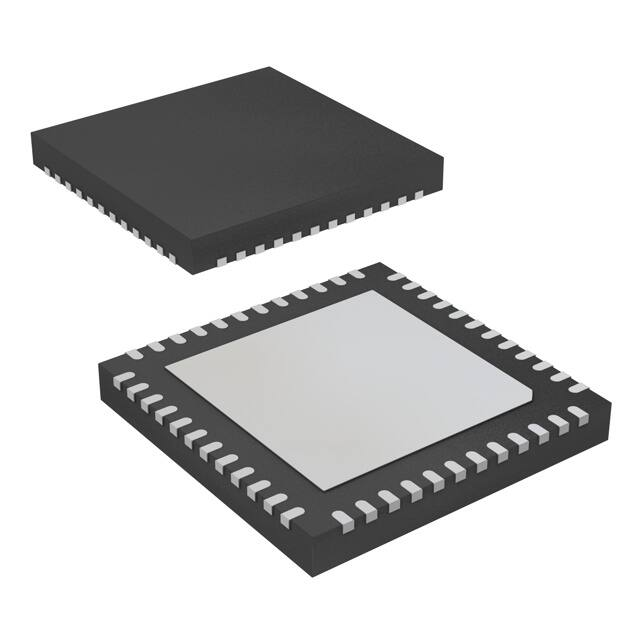


 工商网监
湘ICP备2023018690号
工商网监
湘ICP备2023018690号
