Product
Folder
Order
Now
Support &
Community
Tools &
Software
Technical
Documents
ADS8363, ADS7263, ADS7223
SBAS523D – OCTOBER 2010 – REVISED SEPTEMBER 2017
ADSxxx3 Dual, 1-MSPS, 16-, 14-, and 12-Bit, 4×2 or 2×2 Channel, Simultaneous Sampling
Analog-to-Digital Converter
1 Features
3 Description
•
•
•
The ADS8363 is a dual, 16-bit, 1-MSPS analog-todigital converter (ADC) with eight pseudo- or four
fully-differential input channels grouped into two pairs
for simultaneous signal acquisition. The analog inputs
are maintained differentially to the input of the ADC.
The input multiplexer can be used in either pseudodifferential mode, supporting up to four channels per
ADC (4x2), or in fully-differential mode that allows to
convert up to two inputs per ADC (2x2). The
ADS7263 is a 14-bit version and the ADS7223 is a
12-bit version of the ADS8363.
1
•
•
•
•
•
Eight Pseudo- or Four Fully-Differential Inputs
Simultaneous Sampling of Two Channels
Excellent AC Performance:
– SNR:
93 dB (ADS8363)
85 dB (ADS7263)
73 dB (ADS7223)
– THD:
–98 dB (ADS8363)
–92 dB (ADS7263)
–86 dB (ADS7223)
Dual Programmable and Buffered 2.5-V
Reference Allows:
– Two Different Input Voltage Range Settings
– Two-Level PGA Implementation
Programmable Auto-Sequencer
Integrated Data Storage (up to 4 per channel) for
Oversampling Applications
2-Bit Counter for Safety Applications
Fully Specified Over the Extended Industrial
Temperature Range: –40°C to +125°C
The ADS8363, ADS7263, and ADS7223 offer two
programmable reference outputs, flexible supply
voltage ranges, a programmable auto-sequencer,
data storage of up to four conversion results per
channel, and several power-down features.
All devices are offered in a 5-mm x 5-mm, 32-pin
VQFN package.
Device Information(1)
PART NUMBER
ADSxxx3
•
•
•
•
•
Motor Control: Current and Position Measurement
including Safety Applications
Power Quality Measurement
Three-Phase Power Control
Programmable Logic Controllers
Industrial Automation
Protection Relays
VQFN (32)
BODY SIZE (NOM)
5.00 mm x 5.00 mm
(1) For all available packages, see the package option addendum
at the end of the data sheet.
2 Applications
•
PACKAGE
Functional Block Diagram
AVDD
CHA1P/CHA3
CHA1N/CHA2
CHA0P/CHA1
CHA0N/CHA0
CMA
Input
Mux
DVDD
CLOCK
Serial
Interface
and
FIFO
REF1
REF2
CHB1P/CHB3
CHB1N/CHB2
CHB0P/CHB1
CHB0N/CHB0
CMB
CS
SAR ADC
BUSY
SDI
RD
SDOA
Input
Mux
SAR ADC
SDOB
REF1
String
DAC
REFIO1
2.5V
REF
Control
Logic
M1
CONVST
REF2
REFIO2
M0
String
DAC
RGND
AGND
DGND
1
An IMPORTANT NOTICE at the end of this data sheet addresses availability, warranty, changes, use in safety-critical applications,
intellectual property matters and other important disclaimers. PRODUCTION DATA.
�ADS8363, ADS7263, ADS7223
SBAS523D – OCTOBER 2010 – REVISED SEPTEMBER 2017
www.ti.com
Table of Contents
1
2
3
4
5
6
7
Features ..................................................................
Applications ...........................................................
Description .............................................................
Revision History.....................................................
Device Comparison Table.....................................
Pin Configuration and Functions .........................
Specifications.........................................................
7.1
7.2
7.3
7.4
7.5
7.6
7.7
7.8
7.9
7.10
8
1
1
1
2
4
4
6
Absolute Maximum Ratings ...................................... 6
ESD Ratings.............................................................. 6
Recommended Operating Conditions....................... 6
Thermal Information .................................................. 6
Electrical Characteristics: General ............................ 7
Electrical Characteristics: ADS8363 ......................... 9
Electrical Characteristics: ADS7263 ......................... 9
Electrical Characteristics: ADS7223 ....................... 10
Switching Characteristics ........................................ 11
Typical Characteristics .......................................... 14
Detailed Description ............................................ 18
8.1 Overview ................................................................. 18
8.2 Functional Block Diagram ....................................... 18
8.3
8.4
8.5
8.6
9
Feature Description.................................................
Device Functional Modes........................................
Programming...........................................................
Register Maps .........................................................
19
24
26
34
Application and Implementation ........................ 42
9.1 Application Information............................................ 42
10 Power Supply Recommendations ..................... 45
11 Layout................................................................... 46
11.1 Layout Guidelines ................................................. 46
11.2 Layout Example .................................................... 47
12 Device and Documentation Support ................. 48
12.1
12.2
12.3
12.4
12.5
12.6
12.7
Documentation Support ........................................
Related Links ........................................................
Receiving Notification of Documentation Updates
Community Resources..........................................
Trademarks ...........................................................
Electrostatic Discharge Caution ............................
Glossary ................................................................
48
48
48
48
48
48
48
13 Mechanical, Packaging, and Orderable
Information ........................................................... 49
4 Revision History
Changes from Revision C (January 2017) to Revision D
•
Page
Changed operating temperature from 85°C to 125°C in Recommended Operating Conditions table ................................... 6
Changes from Revision B (January 2011) to Revision C
Page
•
Added Device Information table, ESD Ratings table, Recommended Operating Conditions table, Feature
Description section, Device Functional Modes section, Application and Implementation section, Power Supply
Recommendations section, Layout section, Device and Documentation Support section, and Mechanical,
Packaging, and Orderable Information section ...................................................................................................................... 1
•
Changed ADS8363/7263/7223 to ADS8363, ADS7263, and ADS7223 throughout document ............................................. 1
•
Changed Description section: changed last sentence of first paragraph and last paragraph ............................................... 1
•
Changed Device Comparison Table title ................................................................................................................................ 4
•
Changed Pin Configuration and Functions section title.......................................................................................................... 4
•
Changed footnote of Figure 1 and for clarity ........................................................................................................................ 12
•
Changed second and third columns of Midscale – 1 LSB row in Output Data Format table: changed –VREF to –2VREF
in column 2, changed last two voltage values in column 3 .................................................................................................. 26
•
Changed footnote of Figure 31 ............................................................................................................................................ 27
•
Changed footnote of Figure 32 ............................................................................................................................................ 28
•
Changed footnote of Figure 33 ............................................................................................................................................ 29
•
Changed footnote of Figure 34 ............................................................................................................................................ 30
•
Changed footnote of Figure 35 ............................................................................................................................................ 31
•
Changed footnote of Figure 36 ............................................................................................................................................ 32
•
Changed footnote of Figure 38 ............................................................................................................................................ 34
•
Changed footnote of Figure 40 ............................................................................................................................................ 36
•
Changed 1FFh to 3FFh in bits 9-0 description of REFDAC1 Control Register and REFDAC2 Control Register................ 37
2
Submit Documentation Feedback
Copyright © 2010–2017, Texas Instruments Incorporated
Product Folder Links: ADS8363 ADS7263 ADS7223
�ADS8363, ADS7263, ADS7223
www.ti.com
SBAS523D – OCTOBER 2010 – REVISED SEPTEMBER 2017
Changes from Revision A (December, 2010) to Revision B
Page
•
Revised test conditions for gain error parameter ................................................................................................................... 9
•
Revised test conditions for gain error parameter ................................................................................................................... 9
•
Revised test conditions for gain error parameter ................................................................................................................. 10
•
Updated CONVST high time specification............................................................................................................................ 11
•
Revised CONVST section .................................................................................................................................................... 20
•
Revised Mode II section ....................................................................................................................................................... 28
•
Revised Special Read Mode II section................................................................................................................................. 29
•
Revised Fully-Differential Mode IV section........................................................................................................................... 31
•
Revised Special Mode IV section ......................................................................................................................................... 32
•
Added CONVST section in ADS8361 Compatibility ............................................................................................................. 43
Changes from Original (October, 2010) to Revision A
Page
•
Added RD high time (t3) parameter to Timing Characteristics table .................................................................................... 11
•
Updated Figure 1.................................................................................................................................................................. 12
•
Revised RD section in ADS8361 Compatibility .................................................................................................................... 43
•
Added t3 timing trace to Figure 48........................................................................................................................................ 45
•
Deleted Four-Wire Application Timing Requirements table ................................................................................................. 45
Copyright © 2010–2017, Texas Instruments Incorporated
Product Folder Links: ADS8363 ADS7263 ADS7223
Submit Documentation Feedback
3
�ADS8363, ADS7263, ADS7223
SBAS523D – OCTOBER 2010 – REVISED SEPTEMBER 2017
www.ti.com
5 Device Comparison Table
(1)
PRODUCT
RESOLUTION
NMC
INL
SNR
THD
ADS8363
16 bits
16 or 15 bits (1)
±3 or ±4 LSB (1)
93 dB (typ)
–98 dB (typ)
ADS7263
14 bits
14 bits
±1 LSB
85 dB (typ)
–92 dB (typ)
ADS7223
12 bits
12 bits
±0.5 LSB
73 dB (typ)
–86 dB (typ)
See the Electrical Characteristics table.
6 Pin Configuration and Functions
CMB
CMA
AGND
AVDD
DGND
DVDD
NC
SDOA
32
31
30
29
28
27
26
25
RHB Package
32-Pin VQFN
Top View
CHB1P/CHB3
1
24
SDOB
CHB1N/CHB2
2
23
BUSY
CHB0P/CHB1
3
22
CLOCK
CHB0N/CHB0
4
21
CS
CHA1P/CHA3
5
20
RD
CHA1N/CHA2
6
19
CONVST
CHA0P/CHA1
7
18
SDI
CHA0N/CHA0
8
17
M0
Thermal
9
10
11
12
13
14
15
16
REFIO1
REFIO2
RGND
AGND
AVDD
NC
NC
M1
Pad
Not to scale
Pin Functions
PIN
NAME
NO.
TYPE (1)
AGND
12, 30
P
Analog ground. Connect to analog ground plane.
AVDD
13, 29
P
Analog power supply, 2.7 V to 5.5 V. Decouple to AGND with a 1-μF ceramic capacitor.
BUSY
23
DO
Converter busy indicator. BUSY goes high when the inputs are in hold mode and returns to low after the
conversion is complete.
CHA0N/CHA0
8
AI
Fully-differential inverting analog input channel A1 or pseudo-differential input A0
CHA0P/CHA1
7
AI
Fully-differential noninverting analog input channel A1 or pseudo-differential input A1
CHA1N/CHA2
6
AI
Fully-differential inverting analog input channel A1 or pseudo-differential input A2
CHA1P/CHA3
5
AI
Fully-differential noninverting analog input channel A1 or pseudo-differential input A3
CHB0N/CHB0
4
AI
Fully-differential inverting analog input channel B0 or pseudo-differential input B0
CHB0P/CHB1
3
AI
Fully-differential noninverting analog input channel B0 or pseudo-differential input B1
CHB1N/CHB2
2
AI
Fully-differential inverting analog input channel B1 or pseudo-differential input B2
CHB1P/CHB3
1
AI
Fully-differential noninverting analog input channel B1 or pseudo-differential input B3
(1)
4
DESCRIPTION
AI = analog input, AIO = analog input/output, DI = digital input, DO = digital output, DIO = digital input/output, P = power supply, NC =
not connected.
Submit Documentation Feedback
Copyright © 2010–2017, Texas Instruments Incorporated
Product Folder Links: ADS8363 ADS7263 ADS7223
�ADS8363, ADS7263, ADS7223
www.ti.com
SBAS523D – OCTOBER 2010 – REVISED SEPTEMBER 2017
Pin Functions (continued)
PIN
NAME
NO.
TYPE (1)
DESCRIPTION
CLOCK
22
DI
External clock input. The range is 0.5 MHz to 20 MHz in half-clock mode, or 1 MHz to 40 MHz in full-clock
mode.
CMA
31
AI
Common-mode voltage input for channels Ax (in pseudo-differential mode only).
CMB
32
AI
Common-mode voltage input for channels Bx (in pseudo-differential mode only).
CONVST
19
DI
Conversion start. The ADC switches from sample into hold mode on the rising edge of CONVST. Thereafter,
the conversion starts with the next rising edge of the CLOCK pin.
CS
21
DI
Chip select. When this pin is low, the SDOx, SDI, and RD pins are active; when this pin is high, the SDOx
outputs are 3-stated, and the SDI and RD inputs are ignored.
DGND
28
P
Digital ground. Connect to digital ground plane.
DVDD
27
P
Digital supply, 2.3 V to 5.5 V. Decouple to DGND with a 1-μF ceramic capacitor.
M0
17
DI
Mode pin 0. Selects analog input channel mode (see Table 5).
M1
16
DI
Mode pin 1. Selects the digital output mode (see Table 5).
NC
14, 15, 26
NC
This pin is not internally connected.
RD
20
DI
Read data. Synchronization pulse for the SDOx outputs and SDI input. RD only triggers when CS is low.
REFIO1
9
AIO
Reference voltage input/output 1. A ceramic capacitor of 22 µF connected to RGND is required.
REFIO2
10
AIO
Reference voltage input/output 2. A ceramic capacitor of 22 µF connected to RGND is required.
RGND
11
P
Reference ground. Connect to analog ground plane with a dedicated via.
SDI
18
DI
Serial data input. This pin is used to set up of the internal registers, and can also be used in ADS8361compatible manner. The data on SDI are ignored when CS is high.
SDOA
25
DO
Serial data output for converter A. 3-state when CS is high.
SDOB
24
DO
Serial data output for converter B. Active only if M1 is low. 3-state when CS is high.
Copyright © 2010–2017, Texas Instruments Incorporated
Product Folder Links: ADS8363 ADS7263 ADS7223
Submit Documentation Feedback
5
�ADS8363, ADS7263, ADS7223
SBAS523D – OCTOBER 2010 – REVISED SEPTEMBER 2017
www.ti.com
7 Specifications
7.1 Absolute Maximum Ratings
over operating free-air temperature range (unless otherwise noted) (1)
Supply voltage, AVDD to AGND or DVDD to DGND
MIN
MAX
–0.3
6
Supply voltage, DVDD to AVDD
1.2 × AVDD
UNIT
V
(2)
V
Analog and reference input voltage with respect to AGND
AGND – 0.3
AVDD + 0.3
V
Digital input voltage with respect to DGND
DGND – 0.3
DVDD + 0.3
V
Ground voltage difference |AGND-DGND|
Input current to any pin except supply pins
Maximum virtual junction temperature, TJ
Storage temperature, Tstg
(1)
(2)
0.3
V
10
mA
150
°C
150
°C
–10
–65
Stresses beyond those listed under Absolute Maximum Ratings may cause permanent damage to the device. These are stress ratings
only, which do not imply functional operation of the device at these or any other conditions beyond those indicated under Recommended
Operating Conditions. Exposure to absolute-maximum-rated conditions for extended periods may affect device reliability.
Exceeding the specified limit causes an increase of the DVDD leakage current and leads to malfunction of the device.
7.2 ESD Ratings
VALUE
V(ESD)
(1)
(2)
Electrostatic discharge
Human-body model (HBM), per ANSI/ESDA/JEDEC JS-001 (1)
±2000
Charged-device model (CDM), per JEDEC specification JESD22-C101 (2)
±500
UNIT
V
JEDEC document JEP155 states that 500-V HBM allows safe manufacturing with a standard ESD control process.
JEDEC document JEP157 states that 250-V CDM allows safe manufacturing with a standard ESD control process.
7.3 Recommended Operating Conditions
over operating free-air temperature range (unless otherwise noted)
MIN
AVDD
Analog supply voltage
DVDD
Digital supply voltage
NOM
MAX
5
V
3.3
Operating temperature
–40
UNIT
V
125
°C
7.4 Thermal Information
ADS8363, ADS7263, ADS7223
THERMAL METRIC (1)
RHB (VQFN)
UNIT
32 PINS
RθJA
Junction-to-ambient thermal resistance
33.3
°C/W
RθJC(top)
Junction-to-case (top) thermal resistance
29.5
°C/W
RθJB
Junction-to-board thermal resistance
7.3
°C/W
ψJT
Junction-to-top characterization parameter
0.2
°C/W
ψJB
Junction-to-board characterization parameter
7.4
°C/W
RθJC(bot)
Junction-to-case (bottom) thermal resistance
0.9
°C/W
(1)
6
For more information about traditional and new thermal metrics, see the Semiconductor and IC Package Thermal Metrics application
report.
Submit Documentation Feedback
Copyright © 2010–2017, Texas Instruments Incorporated
Product Folder Links: ADS8363 ADS7263 ADS7223
�ADS8363, ADS7263, ADS7223
www.ti.com
SBAS523D – OCTOBER 2010 – REVISED SEPTEMBER 2017
7.5 Electrical Characteristics: General
All minimum and maximum specifications at TA = –40°C to +125°C, specified supply voltage range, VREF = 2.5 V (int), and
tDATA = 1 MSPS (unless otherwise noted). Typical values are at TA = +25°C, AVDD = 5 V, and DVDD = 3.3 V.
PARAMETER
TEST CONDITIONS
MIN
TYP
MAX
UNIT
+VREF
V
ANALOG INPUT
FSR
Full-scale input range
(CHxxP – CHxxN) or CHxx to
CMx
VIN
Absolute input voltage
CHxxx to AGND
CIN
Input capacitance
CHxxx to AGND
CID
Differential input capacitance
IIL
Input leakage current
PSRR
Power-supply rejection ratio
–VREF
–0.1
AVDD + 0.1
V
45
pF
22.5
–16
AVDD = 5.5 V
pF
16
nA
75
dB
SAMPLING DYNAMICS
tCONV
Conversion time per ADC
tACQ
Acquisition time
fDATA
Data rate
tA
Aperture delay
17.5
Full-clock mode
35
Half-clock mode
2
Full-clock Mode
4
Clock frequency
tCLK
Clock period
tCLK
1000
kSPS
6
ADC to ADC
ns
50
Aperture jitter
fCLK
tCLK
25
tA match
tAJIT
Half-clock mode
ps
50
ps
Half-clock mode
0.5
20
Full-clock mode
1
40
Half-clock mode
50
2000
Full-clock mode
25
1000
MHz
ns
INTERNAL VOLTAGE REFERENCE
Resolution
Reference output DAC resolution
10
Over 20% to 100% DAC range
VREFOUT
Reference output voltage
dVREFOUT/dT
Reference voltage drift
DNLDAC
DAC differential linearity error
INLDAC
DAC integral linearity error
VOSDAC
DAC offset error
PSRR
Power-supply rejection ratio
IREFOUT
Reference output dc current
IREFSC
Reference output short-circuit
current (1)
tREFON
Reference output settling time
Bits
0.2VREFOUT
VREFOUT
REFIO1, DAC = 3FFh
2.485
2.500
2.515
REFIO2, DAC = 3FFh
2.480
2.500
2.520
±10
VREFOUT = 0.5 V
V
ppm/°C
–4
±1
4
LSB
–4
±0.5
4
LSB
–4
±1
4
LSB
73
–2
CREF = 22 μF
dB
+2
mA
50
mA
8
ms
VOLTAGE REFERENCE INPUT
VREF
Reference input voltage range
IREF
Reference input current
50
μA
CREF
External ceramic reference
capacitance
22
μF
(1)
0.5
2.5
2.525
V
Reference output current is not internally limited.
Copyright © 2010–2017, Texas Instruments Incorporated
Product Folder Links: ADS8363 ADS7263 ADS7223
Submit Documentation Feedback
7
�ADS8363, ADS7263, ADS7223
SBAS523D – OCTOBER 2010 – REVISED SEPTEMBER 2017
www.ti.com
Electrical Characteristics: General (continued)
All minimum and maximum specifications at TA = –40°C to +125°C, specified supply voltage range, VREF = 2.5 V (int), and
tDATA = 1 MSPS (unless otherwise noted). Typical values are at TA = +25°C, AVDD = 5 V, and DVDD = 3.3 V.
PARAMETER
TEST CONDITIONS
MIN
TYP
MAX
UNIT
+50
nA
DIGITAL INPUTS (2)
IIN
Input current
CIN
Input capacitance
VIN = DVDD to DGND
–50
5
Logic family
pF
CMOS with Schmitt-Trigger
VIH
High-level input voltage
DVDD = 4.5 V to 5.5 V
0.7DVDD
DVDD + 0.3
V
VIL
Low-level input voltage
DVDD = 4.5 V to 5.5 V
–0.3
0.3DVDD
V
Logic family
LVCMOS
VIH
High-level input voltage
DVDD = 2.3 V to 3.6 V
2
DVDD + 0.3
V
VIL
Low-level input voltage
DVDD = 2.3 V to 3.6 V
–0.3
0.8
V
DIGITAL OUTPUTS (2)
COUT
Output capacitance
CLOAD
Load capacitance
5
pF
30
Logic family
pF
CMOS
VOH
High-level output voltage
DVDD = 4.5 V, IOH = –100 µA
VOL
Low-level output voltage
DVDD = 4.5 V, IOH = +100 µA
4.44
V
0.5
Logic family
V
LVCMOS
VOH
High-level output voltage
DVDD = 2.3 V, IOH = –100 µA
VOL
Low-level output voltage
DVDD = 2.3 V, IOH = +100 µA
DVDD – 0.2
V
0.2
V
POWER SUPPLY
AVDD
Analog supply voltage
DVDD
Digital supply voltage
AIDD
Analog supply current
AVDD to AGND, half-clock mode
2.7
5.0
5.5
AVDD to AGND, full-clock mode
4.5
5.0
5.5
3-V and 3.3-V levels
2.3
2.5
3.6
5-V levels, half-clock mode only
4.5
5.0
5.5
AVDD = 3.6 V
12.0
16.0
AVDD = 5.5 V
15.0
20.0
AVDD = 3.6 V, sleep and autosleep modes
0.8
1.2
AVDD = 5.5 V, sleep and autosleep modes
0.9
1.4
Power-down mode
DIDD
Digital supply current
PD
Power dissipation (normal
operation)
(2)
8
V
V
mA
0.005
DVDD = 3.6 V, CLOAD = 10 pF
1.1
2.5
DVDD = 5.5 V, CLOAD = 10 pF
3
6
AVDD = DVDD = 3.6 V
47.2
66.6
AVDD = 5.5 V, DVDD = 3.6 V
86.5
117.0
mA
mW
Specified by design; not production tested.
Submit Documentation Feedback
Copyright © 2010–2017, Texas Instruments Incorporated
Product Folder Links: ADS8363 ADS7263 ADS7223
�ADS8363, ADS7263, ADS7223
www.ti.com
SBAS523D – OCTOBER 2010 – REVISED SEPTEMBER 2017
7.6 Electrical Characteristics: ADS8363
All minimum and maximum specifications at TA = –40°C to +125°C, specified supply voltage range, VREF = 2.5 V (int), and
tDATA = 1 MSPS (unless otherwise noted). Typical values are at TA = +25°C, AVDD = 5 V, and DVDD = 3.3 V.
PARAMETER
TEST CONDITIONS
MIN
TYP
MAX
UNIT
RESOLUTION
Resolution
16
Bits
DC ACCURACY
INL
Integral nonlinearity
DNL
Differential nonlinearity
VOS
Input offset error
VOS match
Half-clock mode
–3
±1.2
+3
Full-clock mode
–4
±1.5
+4
Half-clock mode
–0.99
±0.6
+2
Full-clock mode
–1.5
±0.8
+3
–2
±0.2
+2
–1
±0.1
+1
ADC to ADC
dVOS/dT
Input offset thermal drift
1
GERR
Gain error
Referenced to the voltage at
REFIOx
–0.1%
±0.01%
+0.1%
GERR match
ADC to ADC
–0.1%
±0.005%
+0.1%
GERR/dT
Gain error thermal drift
Referenced to the voltage at
REFIOx
CMRR
Common-mode rejection ratio
Both ADCs, dc to 100 kHz
LSB
LSB
mV
mV
μV/°C
1
ppm/°C
92
dB
92
dB
AC ACCURACY
SINAD
Signal-to-noise + distortion
VIN = 5 VPP at 10 kHz
89
SNR
Signal-to-noise ratio
VIN = 5 VPP at 10 kHz
90
THD
Total harmonic distortion
VIN = 5 VPP at 10 kHz
SFDR
Spurious-free dynamic range
VIN = 5 VPP at 10 kHz
93
–98
90
dB
–90
dB
100
dB
7.7 Electrical Characteristics: ADS7263
All minimum and maximum specifications at TA = –40°C to +125°C, specified supply voltage range, VREF = 2.5 V (int), and
tDATA = 1 MSPS (unless otherwise noted). Typical values are at TA = +25°C, AVDD = 5 V, and DVDD = 3.3 V.
PARAMETER
TEST CONDITIONS
MIN
TYP
MAX
UNIT
RESOLUTION
Resolution
14
Bits
DC ACCURACY
INL
Integral nonlinearity
DNL
Differential nonlinearity
VOS
Input offset error
VOS match
–1
±0.4
+1
LSB
–0.5
±0.2
+1
LSB
–2
±0.2
+2
mV
–1
±0.1
+1
ADC to ADC
dVOS/dT
Input offset thermal drift
1
GERR
Gain error
Referenced to the voltage at
REFIOx
–0.1%
±0.01%
+0.1%
GERR match
ADC to ADC
–0.1%
±0.005%
+0.1%
GERR/dT
Gain error thermal drift
Referenced to the voltage at
REFIOx
CMRR
Common-mode rejection ratio
Both ADCs, dc to 100 kHz
mV
μV/°C
1
ppm/°C
92
dB
AC ACCURACY
SINAD
Signal-to-noise + distortion
VIN = 5 VPP at 10 kHz
82
84
dB
SNR
Signal-to-noise ratio
VIN = 5 VPP at 10 kHz
84
85
dB
THD
Total harmonic distortion
VIN = 5 VPP at 10 kHz
SFDR
Spurious-free dynamic range
VIN = 5 VPP at 10 kHz
Copyright © 2010–2017, Texas Instruments Incorporated
Product Folder Links: ADS8363 ADS7263 ADS7223
–92
88
–88
92
Submit Documentation Feedback
dB
dB
9
�ADS8363, ADS7263, ADS7223
SBAS523D – OCTOBER 2010 – REVISED SEPTEMBER 2017
www.ti.com
7.8 Electrical Characteristics: ADS7223
All minimum and maximum specifications at TA = –40°C to +125°C, specified supply voltage range, VREF = 2.5 V (int), and
tDATA = 1 MSPS (unless otherwise noted). Typical values are at TA = +25°C, AVDD = 5 V, and DVDD = 3.3 V.
PARAMETER
TEST CONDITIONS
MIN
TYP
MAX
UNIT
RESOLUTION
Resolution
12
Bits
DC ACCURACY
INL
Integral nonlinearity
–0.5
±0.2
+0.5
LSB
DNL
Differential nonlinearity
–0.5
±0.1
+0.5
LSB
VOS
Input offset error
–2
±0.2
+2
mV
–1
±0.1
+1
VOS match
ADC to ADC
dVOS/dT
Input offset thermal drift
1
GERR
Gain error
Referenced to the voltage at
REFIOx
–0.1%
±0.01%
+0.1%
GERR match
ADC to ADC
–0.1%
±0.005%
+0.1%
GERR/dT
Gain error thermal drift
Referenced to the voltage at
REFIOx
CMRR
Common-mode rejection ratio
Both ADCs, dc to 100 kHz
mV
μV/°C
1
ppm/°C
92
dB
dB
AC ACCURACY
SINAD
Signal-to-noise + distortion
VIN = 5 VPP at 10 kHz
71
72
SNR
Signal-to-noise ratio
VIN = 5 VPP at 10 kHz
72
73
THD
Total harmonic distortion
VIN = 5 VPP at 10 kHz
SFDR
Spurious-free dynamic range
VIN = 5 VPP at 10 kHz
10
Submit Documentation Feedback
–86
84
86
dB
–84
dB
dB
Copyright © 2010–2017, Texas Instruments Incorporated
Product Folder Links: ADS8363 ADS7263 ADS7223
�ADS8363, ADS7263, ADS7223
www.ti.com
SBAS523D – OCTOBER 2010 – REVISED SEPTEMBER 2017
7.9 Switching Characteristics (1)
Over the recommended operating free-air temperature range of –40°C to +125°C, and DVDD = 2.3 V to 5.5 V (unless
otherwise noted).
MIN
tDATA
Data throughput, fCLK = max
tCONV
Conversion time
tACQ
Acquisition time
MAX
1
Half-clock mode
17.5
Full-clock mode
35
UNIT
μs
tCLK
100
ns
Half-clock mode
0.5
20
Full-clock mode
1
40
Half-clock mode
50
2000
Full-clock mode
25
1000
fCLK
CLOCK frequency
tCLK
CLOCK period
tCLKL
CLOCK low time
11.25
ns
tCLKH
CLOCK high time
11.25
ns
t1
CONVST rising edge to first CLOCK rising edge
12
ns
10
ns
t2
CONVST high time
t3
RD high time, half-clock mode: timing modes II, IV, SII, and SIV only
tS1
RD high to CLOCK falling edge setup time
5
ns
tH1
RD high to CLOCK falling edge hold time
5
ns
tS2
Input data to CLOCK falling edge setup time
5
ns
tH2
Input data to CLOCK falling edge hold time
Half-clock mode: timing
modes II and IV only
tD1
CONVST rising edge to BUSY high delay (2)
tD2
CLOCK 18th falling edge (half-clock mode) or
24th rising edge (full-clock mode) to BUSY low
delay
tD3
CLOCK rising edge to next data valid delay
2.3 V < DVDD < 3.6 V
25
4.5 V < DVDD < 5.5 V
20
Half-clock mode,
2.3 V < DVDD < 3.6 V
14
Half-clock mode,
4.5 V < DVDD < 5.5 V
12
Output data to CLOCK falling edge hold time, full-clock mode
CS rising edge to SDOx 3-state
(1)
(2)
ns
16
CLOCK falling edge to next data valid delay, full-clock mode
tD6
tCLK
4.5 V < DVDD < 5.5 V
tH4
RD falling edge to first data valid
1
19
tD4
tD5
tCLK
4
Output data to CLOCK rising edge hold time, half-clock mode
ns
1
2.3 V < DVDD < 3.6 V
tH3
MHz
ns
ns
ns
3
ns
19
7
ns
ns
2.3 V < DVDD < 3.6 V
16
4.5 V < DVDD < 5.5 V
12
6
ns
ns
All input signals are specified with tR = tF = 1.5 ns (10% to 90% of DVDD) and timed from a voltage level of (VIL + VIH) / 2.
Not applicable in auto-sleep power-down mode.
Copyright © 2010–2017, Texas Instruments Incorporated
Product Folder Links: ADS8363 ADS7263 ADS7223
Submit Documentation Feedback
11
�ADS8363, ADS7263, ADS7223
SBAS523D – OCTOBER 2010 – REVISED SEPTEMBER 2017
tCLK
www.ti.com
tCLKL
1
tCLKH
18
21
CLOCK
tCONV
tACQ
CS
t1
t2
CONVST
tDATA
tD2
tD1
BUSY
conversion n
tH1
tS1
t3
RD
tD5
SDOx(1)
(CID = ‘0’)
tH3
data n-1
CH
AD
0/1
A/B
MSB
D14
D13
D12
D11
D10
D9
tD6
tD3
D8
D7
D6
D5
D4
D3
D2
D6
D5
D4
D3
D2
D1
D0
D1
D0
CH
0/1
data n-1
SDOx(1)
(CID = ‘1’)
MSB
D14
D13
D12
D11
tS2
SDI
D15
(1)
D14
D13
D10
D9
D8
D7
MSB
tH2
D12
D11
D10
D9
D8
D7
D6
D5
D4
D3
D2
D1
D0
D15
The ADS7263 and ADS7223 output data with the MSB located as the ADS8363 and the last 2 or 4 bits are '0'.
Figure 1. Detailed Timing Diagram: Half-Clock Mode (ADS8361-Compatible)
12
Submit Documentation Feedback
Copyright © 2010–2017, Texas Instruments Incorporated
Product Folder Links: ADS8363 ADS7263 ADS7223
�ADS8363, ADS7263, ADS7223
www.ti.com
SBAS523D – OCTOBER 2010 – REVISED SEPTEMBER 2017
tCLK
1
tCLKL
tCLKH
23
25
36
41
CLOCK
tCONV
tACQ
CS
tDATA
t1
t2
CONVST
tD2
tD1
BUSY
conversion n
tH1
tS1
RD
tD5
(CID = ‘0’)
tH4
M
CH AD
0/1 A/B S
B
SDOx(1)
D
14
data n
D
13
D
12
D
11
D
10
tD4
D9 D8 D7 D6 D5 D4 D3 D0 D1 D0
tS2
D
15
SDI
D
14
D
13
D
12
D
11
D
10
tD6
tH2
D9 D8 D7 D6 D5 D4 D3 D2 D1 D0
RD
tD5
(CID = ‘1’)
SDOx(1)
data n
tH4
M
S
B
D
14
D
13
D
12
D
11
D
10
D9 D8 D7 D6 D5 D4 D3 D2 D1 D0
tS2
D
15
SDI
(2)
D
14
D
13
D
12
tD4
tH2
D
11
D
10
D9 D8 D7 D6 D5 D4 D3 D2 D1 D0
The ADS7263 and ADS7223 output data with the MSB located as the ADS8363 and the last 2 or 4 bits are '0'.
Figure 2. Detailed Timing Diagram: Full-Clock Mode
Copyright © 2010–2017, Texas Instruments Incorporated
Product Folder Links: ADS8363 ADS7263 ADS7223
Submit Documentation Feedback
13
�ADS8363, ADS7263, ADS7223
SBAS523D – OCTOBER 2010 – REVISED SEPTEMBER 2017
www.ti.com
7.10 Typical Characteristics
at TA = +25°C, AVDD = 5 V, DVDD = 3.3 V, VREF = 2.5 V (internal), and fDATA = 1 MSPS (unless otherwise noted)
3.0
3.0
ADS8363 Positive
ADS7263 Positive
ADS7223 Positive
2.5
2.0
1.5
1.5
1.0
1.0
0.5
0
-0.5
-1.0
-1.5
200
300
400 500 600 700
Data Rate (kSPS)
800
900
0
-0.5
-1.0
ADS8363 Negative
ADS7263 Negative
ADS7223 Negative
-2.5
-3.0
-3.0
100
0.5
-1.5
-2.0
ADS8363 Negative
ADS7263 Negative
ADS7223 Negative
-2.0
-2.5
ADS8363 Positive
ADS7263 Positive
ADS7223 Positive
2.5
DNL (LSB)
INL (LSB)
2.0
1000
100
Figure 3. Integral Nonlinearity vs Data Rate
3.0
1.5
1.0
1.0
DNL (LSB)
INL (LSB)
2.0
-0.5
-1.0
-2.5
-3.0
8192 16384 24576 32768 40960 49152 57344 65536
Code
0
Figure 5. Integral Nonlinearity vs Code
2.5
2.0
1.5
1.5
1.0
1.0
0.5
0
-0.5
-1.0
-1.5
-2.0
-2.5
-3.0
5
80
95
110 125
Figure 7. Integral Nonlinearity vs Temperature
Submit Documentation Feedback
-0.5
-1.0
-2.5
-3.0
20 35 50 65
Temperature (°C)
ADS8363
AVDD = 5V, Positive
AVDD = 3V, Positive
0.5
0
-1.5
-2.0
AVDD = 5V, Negative
AVDD = 3V, Negative
-40 -25 -10
14
3.0
DNL (LSB)
INL (LSB)
2.0
8192 16384 24576 32768 40960 49152 57344 65536
Code
Figure 6. Differential Nonlinearity vs Code
ADS8363
AVDD = 5V, Positive
AVDD = 3V, Positive
ADS8363
0
-2.5
-3.0
2.5
1000
-0.5
-1.0
-1.5
-2.0
3.0
900
0.5
-1.5
-2.0
0
800
2.5
1.5
0
400 500 600 700
Data Rate (kSPS)
3.0
2.0
0.5
300
Figure 4. Differential Nonlinearity vs Data Rate
ADS8363
2.5
200
AVDD = 5V, Negative
AVDD = 3V, Negative
-40 -25 -10
5
20 35 50 65
Temperature (°C)
80
95
110 125
Figure 8. Differential Nonlinearity vs Temperature
Copyright © 2010–2017, Texas Instruments Incorporated
Product Folder Links: ADS8363 ADS7263 ADS7223
�ADS8363, ADS7263, ADS7223
www.ti.com
SBAS523D – OCTOBER 2010 – REVISED SEPTEMBER 2017
Typical Characteristics (continued)
at TA = +25°C, AVDD = 5 V, DVDD = 3.3 V, VREF = 2.5 V (internal), and fDATA = 1 MSPS (unless otherwise noted)
2.0
2.0
All Devices
Offset Error
Offset Match
1.5
Offset Error and Match (mV)
Offset Error and Match (mV)
All Devices
1.0
0.5
0
-0.5
-1.0
0.5
0
-0.5
-1.0
-2.0
-2.0
2.7
3.1
3.5
3.9
4.3
AVDD (V)
4.7
5.1
5.5
-40 -25 -10
Figure 9. Offset Error and Offset Match vs
Analog Supply Voltage
5
20 35 50 65
Temperature (°C)
80
95
110 125
Figure 10. Offset Error and Offset Match vs Temperature
0.10
0.10
All Devices
0.08
Gain Error
Gain Match
0.06
0.08
Gain Error and Match (%)
Gain Error and Match (%)
1.0
-1.5
-1.5
0.04
0.02
0
-0.02
-0.04
-0.06
All Devices
Gain Error
Gain Match
0.06
0.04
0.02
0
-0.02
-0.04
-0.06
-0.08
-0.08
-0.10
-0.10
2.7
3.1
3.5
3.9
4.3
AVDD (V)
4.7
5.1
5.5
5
-40 -25 -10
Figure 11. Gain Error and Gain Match vs
Analog Supply Voltage
20 35 50 65
Temperature (°C)
80
95
110 125
Figure 12. Gain Error and Gain Match vs Temperature
100
100
95
95
90
90
CMRR (dB)
CMRR (dB)
Offset Error
Offset Match
1.5
85
80
85
80
75
75
All devices
f = 100kHz
70
2.7
3.1
3.5
3.9
4.3
AVDD (V)
4.7
5.1
Figure 13. Common-Mode Rejection Ratio vs
Analog Supply Voltage
5.5
All devices
f = 100kHz
70
-40 -25 -10
5
20 35 50 65
Temperature (°C)
80
95
110 125
Figure 14. Common-Mode Rejection Ratio vs Temperature
Copyright © 2010–2017, Texas Instruments Incorporated
Product Folder Links: ADS8363 ADS7263 ADS7223
Submit Documentation Feedback
15
�ADS8363, ADS7263, ADS7223
SBAS523D – OCTOBER 2010 – REVISED SEPTEMBER 2017
www.ti.com
Typical Characteristics (continued)
at TA = +25°C, AVDD = 5 V, DVDD = 3.3 V, VREF = 2.5 V (internal), and fDATA = 1 MSPS (unless otherwise noted)
0
0
All Devices
-20
-40
-40
-60
-60
Amplitude (dB)
Amplitude (dB)
All Devices
-20
-80
-100
-120
-120
-140
-140
-160
-160
-180
-180
50
100 150 200 250 300 350 400 450 500
Frequency (kHz)
0
Figure 15. Frequency Spectrum
(4096 Point FFT; fIN = 10 kHz)
Figure 16. Frequency Spectrum
(4096 Point FFT; fIN = 10 kHz, fSAMPLE = 0.5 MSPS)
100
100
95
95
90
90
SNR and SINAD (dB)
SNR and SINAD (dB)
0
85
80
75
70
65
60
100
150
Frequency (kHz)
200
250
80
75
70
65
ADS8363 SNR
ADS7263 SNR
ADS7223 SNR
55
ADS8363 SINAD
ADS7263 SINAD
ADS7223 SINAD
50
50
10
20
30
fIN (kHz)
40
-40 -25 -10
50
5
20 35 50 65
Temperature (°C)
80
95
110 125
Figure 18. Signal-to-Noise Ratio and Signal-to-Noise +
Distortion vs Temperature
Figure 17. Signal-to-Noise Ratio and Signal-to-Noise +
Distortion vs Input Signal Frequency
-80
-80
ADS8363
ADS7263
ADS7223
-84
ADS8363
ADS7263
ADS7223
-84
-88
-88
THD (dB)
THD (dB)
50
85
60
ADS8363 SINAD
ADS7263 SINAD
ADS7223 SINAD
ADS8363 SNR
ADS7263 SNR
ADS7223 SNR
55
-92
-92
-96
-96
-100
-100
-104
-104
10
20
30
fIN (kHz)
40
Figure 19. Total Harmonic Distortion vs
Input Signal Frequency
16
-80
-100
Submit Documentation Feedback
50
fIN = 10kHz
-40 -25 -10
5
20 35 50 65
Temperature (°C)
80
95
110 125
Figure 20. Total Harmonic Distortion vs Temperature
Copyright © 2010–2017, Texas Instruments Incorporated
Product Folder Links: ADS8363 ADS7263 ADS7223
�ADS8363, ADS7263, ADS7223
www.ti.com
SBAS523D – OCTOBER 2010 – REVISED SEPTEMBER 2017
Typical Characteristics (continued)
at TA = +25°C, AVDD = 5 V, DVDD = 3.3 V, VREF = 2.5 V (internal), and fDATA = 1 MSPS (unless otherwise noted)
105
104
ADS8363
ADS7263
ADS7223
100
ADS8363
ADS7263
ADS7223
101
99
SFDR (dB)
96
SFDR (dB)
fIN = 10kHz
103
92
97
95
93
88
91
89
84
87
85
80
10
20
30
fIN (kHz)
40
Figure 21. Spurious-Free Dynamic Range vs
Input Signal Frequency
20
AVDD = 5.5V
AVDD = 3.6V
14
IDVDD (mA)
16
14
10
8
80
95
110 125
All Devices
DVDD = 5.5V
DVDD = 3.6V
12
10
8
6
6
4
4
2
2
0
0
-40 -25 -10
5
20 35 50 65
Temperature (°C)
80
95
110 125
-40 -25 -10
Figure 23. Analog Supply Current vs Temperature
5
20 35 50 65
Temperature (°C)
80
95
110 125
Figure 24. Digital Supply Current vs Temperature
20
20
All Devices
18
External Reference
Internal Reference
16
16
14
14
12
10
8
All Devices in Auto-Sleep Mode
18
IAVDD (mA)
IAVDD (mA)
20 35 50 65
Temperature (°C)
18
16
12
5
Figure 22. Spurious-Free Dynamic Range vs Temperature
20
All Devices
18
IAVDD (mA)
-40 -25 -10
50
External Reference
Internal Reference
12
10
8
6
6
4
4
2
2
0
0
0
100 200 300 400 500 600 700 800 900 1000
fSAMPLE (kSPS)
Figure 25. Analog Supply Current vs Data Rate
0
100
200
300
400
500
fSAMPLE (kSPS)
600
700
800
Figure 26. Analog Supply Current vs Data Rate
(Auto-Sleep Mode)
Copyright © 2010–2017, Texas Instruments Incorporated
Product Folder Links: ADS8363 ADS7263 ADS7223
Submit Documentation Feedback
17
�ADS8363, ADS7263, ADS7223
SBAS523D – OCTOBER 2010 – REVISED SEPTEMBER 2017
www.ti.com
8 Detailed Description
8.1 Overview
The ADS8363, ADS7263, and ADS7223 contain two 16-, 14-, and 12-bit analog-to-digital converters (ADCs),
respectively, that operate based on the successive approximation register (SAR) principle. These ADCs sample
and convert simultaneously. Conversion time can be as low as 875 ns. Adding an acquisition time of 100 ns, and
a margin of 25 ns for propagation delay and CONVST pulse generation, results in a maximum conversion rate of
1 MSPS.
Each ADC has a fully-differential 2:1 multiplexer front-end. In many common applications, all negative input
signals remain at the same constant voltage (for example, 2.5 V). For these applications, the multiplexer can be
used in a pseudo-differential 4:1 mode, where the CMx pins function as common-mode pins and all four analog
inputs are referred to the corresponding CMx pin.
The ADS8363, ADS7263, and ADS7223 also include a 2.5-V internal reference. This reference drives two
independently-programmable, 10-bit digital-to-analog converters (DACs), allowing the voltage at each of the
REFIOx pins to be adjusted through the internal REFDACx registers in 2.44-mV steps. A low-noise, unity-gain
operational amplifier buffers each of the DAC outputs and drives the REFIOx pin.
The ADS8363, ADS7263, and ADS7223 provide a serial interface that is compatible with the ADS8361.
However, instead of the ADS8361 A0 pin that controls the channel selection, the ADS8363, ADS7263, and
ADS7223 offers a serial data input (SDI) pin that supports additional functions described in the Digital section of
this data sheet (also see the section).
8.2 Functional Block Diagram
AVDD
CHA1P/CHA3
CHA1N/CHA2
CHA0P/CHA1
CHA0N/CHA0
CMA
Input
Mux
DVDD
CLOCK
Serial
Interface
and
FIFO
REF1
REF2
CHB1P/CHB3
CHB1N/CHB2
CHB0P/CHB1
CHB0N/CHB0
CMB
CS
SAR ADC
BUSY
SDI
RD
SDOA
Input
Mux
SAR ADC
SDOB
REF1
String
DAC
REFIO1
2.5V
REF
Control
Logic
String
DAC
RGND
18
Submit Documentation Feedback
M1
CONVST
REF2
REFIO2
M0
AGND
DGND
Copyright © 2010–2017, Texas Instruments Incorporated
Product Folder Links: ADS8363 ADS7263 ADS7223
�ADS8363, ADS7263, ADS7223
www.ti.com
SBAS523D – OCTOBER 2010 – REVISED SEPTEMBER 2017
8.3 Feature Description
8.3.1 Analog
This section discusses the analog input circuit, the ADCs, and the reference design of the device.
8.3.1.1 Analog Inputs
Each ADC is fed by an input multiplexer, as shown in Figure 27. Each multiplexer is used in either a fullydifferential 2:1 configuration (as shown in Table 1) or a pseudo-differential 4:1 configuration (as shown in
Table 2).
CHx1P/CHx3
CHx1N/CHx2
CHx0P/CHx1
Input
Mux
To
ADC
CHx0N/CHx0
Figure 27. Input Multiplexer Configuration
Channel selection is performed using either the external M0 pin or the C[1:0] bits in the Configuration (CONFIG)
register in fully-differential mode, or using the SEQFIFO register in pseudo-differential mode. In either case,
changing the multiplexer settings impacts the conversion started with the next CONVST pulse.
Table 1. Fully-Differential 2:1 Multiplexer Configuration
C1
C0
ADC+
ADC–
0
x
CHx0P
CHx0N
1
x
CHx1P
CHx1N
Table 2. Pseudo-Differential 4:1 Multiplexer Configuration
C1
C0
ADC+
ADC–
0
0
CHx0
CMx/REFIOx
0
1
CHx1
CMx/REFIOx
1
0
CHx2
CMx/REFIOx
1
1
CHx3
CMx/REFIOx
The input path for the converter is fully differential and provides a good common-mode rejection of 92 dB at
100 kHz (for the ADS8363). The high CMRR also helps suppress noise in harsh industrial environments.
Each of the 40-pF sample-and-hold capacitors (CS in Figure 28) is connected through switches to the multiplexer
output. Opening the switches holds the sampled data during the conversion process. After the conversion
completes, both capacitors are precharged for the duration of one clock cycle to the voltage present at the
REFIOx pin. After precharging, the multiplexer outputs are connected to the sampling capacitors again. The
voltage at the analog input pin is usually different from the reference voltage; therefore, the sample capacitors
must be charged to within one-half LSB for 16-, 14-, or 12-bit accuracy during the acquisition time tACQ (see
Figure 1 and Figure 2).
AVDD
RSER
100W
CHxx+
RSW
100W
CPAR
5pF AVDD
CPAR
5pF
CS
40pF
RSER
AGND 100W
RSW
100W
CS
40pF
CHxx-
AGND
Figure 28. Equivalent Analog Input Circuit
Copyright © 2010–2017, Texas Instruments Incorporated
Product Folder Links: ADS8363 ADS7263 ADS7223
Submit Documentation Feedback
19
�ADS8363, ADS7263, ADS7223
SBAS523D – OCTOBER 2010 – REVISED SEPTEMBER 2017
www.ti.com
Feature Description (continued)
Acquisition is indicated with the BUSY signal being low. Acquisition starts by closing the input switches (after
finishing the previous conversion and precharging) and finishes with the rising edge of the CONVST signal. If the
device operates at full speed, the acquisition time is typically 100 ns.
The minimum –3-dB bandwidth of the driving operational amplifier can be calculated as shown in Equation 1,
with n = 16 for the resolution of the ADS8363, n = 14 for the ADS7263, or n = 12 for the ADS7223:
ln(2)(n + 1)
f-3dB =
2ptACQ
(1)
With tACQ = 100 ns, the minimum bandwidth of the driving amplifier is 19 MHz for the ADS8363, 17 MHz for the
ADS7263, and 15 MHz for the ADS7223. The required bandwidth can be lower if the application allows a longer
acquisition time.
A gain error occurs if a given application does not fulfill the settling requirement shown in Equation 1. However,
linearity and THD are not directly affected as a result of precharging the capacitors.
The OPA365 from Texas Instruments is recommended as a driver; in addition to offering the required bandwidth,
the OPA365 also provides a low offset and excellent THD performance (see the Application and Implementation
section).
The phase margin of the driving operational amplifier is usually reduced by the ADC sampling capacitor. A
resistor placed between the capacitor and the amplifier limits this effect; therefore, an internal 100-Ω resistor
(RSER) is placed in series with the switch. The switch resistance (RSW) is typically 100 Ω; see Figure 28).
An input driver may not be required, if the impedance of the signal source (RSOURCE) fulfills the requirement of
Equation 2:
tACQ
RSOURCE <
- (RSER + RSW)
CSln(2)(n + 1)
where
•
•
•
•
n = 16, 14, 12 for the resolution of the ADS8363, ADS7263, and ADS7223, respectively
CS = 40-pF sample capacitance
RSER = 100-Ω input resistor value
RSW = 100-Ω switch resistance value
(2)
With tACQ = 100 ns, the maximum source impedance must be less than 12 Ω for the ADS8363, less than 40 Ω for
the ADS7263, and less than 77 Ω for the ADS7223. The source impedance can be higher if the ADC is used at a
lower data rate.
The differential input voltage range of the ADC is ±VREF, the voltage at the selected REFIOx pin.
The voltage to all inputs must be kept within the 0.3-V limit below AGND and above AVDD, without allowing dc
current to flow through the inputs (exceeding these limits causes the internal ESD diodes to conduct, leading to
increased leakage current that may damage the device). Current is only necessary to recharge the sample-andhold capacitors.
Unused inputs must be directly tied to AGND or RGND without the need of a pull-down resistor.
8.3.1.2 Analog-to-Digital Converters (ADCs)
The ADS8363, ADS7263, and ADS7223 include two SAR-type, 1 MSPS, 16-, 14-, and 12-bit ADCs that include
sample-and-hold, respectively; see the Functional Block Diagram section.
8.3.1.3 CONVST
The analog inputs are held with the rising edge of the CONVST (conversion start) signal. The setup time of
CONVST referred to the next rising edge of CLOCK (system clock) is 12 ns (minimum). The conversion
automatically starts with the rising CLOCK edge. Do not issue a rising edge of CONVST during a conversion
(that is, when BUSY is high).
20
Submit Documentation Feedback
Copyright © 2010–2017, Texas Instruments Incorporated
Product Folder Links: ADS8363 ADS7263 ADS7223
�ADS8363, ADS7263, ADS7223
www.ti.com
SBAS523D – OCTOBER 2010 – REVISED SEPTEMBER 2017
Feature Description (continued)
RD (read data) and CONVST can be shorted to minimize necessary software and wiring. The RD signal is
triggered by the device on the falling edge of CLOCK. Therefore, the combined signals must be activated with
the rising CLOCK edge. The conversion then starts with the subsequent rising CLOCK edge. In modes with only
SDOA active (that is, in modes II, IV, SII, and SIV), the maximum length of the combined RD and CONVST
signal is one clock cycle if the half-clock timing is used.
If CONVST and RD are combined, CS must be low whenever a new conversion starts; however, this condition is
not required if RD and CONVST are controlled separately. Note that if FIFO is used, CONVST must be
controlled separately from RD.
After completing a conversion, the sample capacitors are automatically precharged to the value of the reference
voltage used to significantly reduce the crosstalk among the multiplexed input channels.
8.3.1.4 CLOCK
The ADS8363, ADS7263, and ADS7223 use an external clock with an allowable frequency range that depends
on the mode being used. By default (after power-up), the ADC operates in half-clock mode that supports a clock
in the range of 0.5 MHz to 20 MHz. In full-clock mode, the ADC requires a clock in the range of 1 MHz to
40 MHz. For maximum data throughput, the clock signal must be continuously running. However, in applications
that use the device in burst mode, the clock can be held static low or high upon completion of the read access
and before starting a new conversion.
The CLOCK duty cycle must be 50%. However, the device functions properly with a duty cycle between 30% and
70%.
8.3.1.5 RESET
The ADS8363, ADS7263, and ADS7223 feature an internal power-on reset (POR) function. A user-controlled
reset can also be issued using SDI register bits A[3:0] (see the Digital section).
8.3.1.6 REFIOx
The ADS8363, ADS7263, and ADS7223 include a low-drift, 2.5-V internal reference source. This source feeds
two, 10-bit string DACs that are controlled through registers. As a result of this architecture, the reference
voltages at REFIOx are programmable in 2.44-mV steps and can be adjusted to the application requirements
without the use of additional external components. The actual output voltage can be calculated using Equation 3,
with code being the decimal value of the REFDACx register content:
2.5V(code +1)
VREF =
1024
(3)
The reference DAC has a fixed transition at the code 508 (0x1FC). At this code, the DAC can show a jump of up
to 10 mV in the transfer function. Table 3 lists some examples of internal reference DAC settings. However, to
ensure proper performance, the REFDACx output voltage must not be programmed below 0.5 V.
Table 3. REFDACx Setting Examples
VREFOUT (NOM)
DECIMAL CODE
BINARY CODE
HEXADECIMAL
CODE
0.5000 V
205
00 1100 1101
0CDh
1.2429 V
507
01 1111 1100
1FBh
1.2427 V
508
01 1111 1101
1FCh
2.5000 V
1023
11 1111 1111
3FFh
A minimum of 22-μF capacitance is required on each REFIOx output to keep the references stable. The settling
time is 8 ms (maximum) with the reference capacitor connected. Smaller reference capacitance values reduce
the DNL, INL, and ac performance of the device. By default, both reference outputs are disabled and the
respective values are set to 2.5 V after power-up.
Copyright © 2010–2017, Texas Instruments Incorporated
Product Folder Links: ADS8363 ADS7263 ADS7223
Submit Documentation Feedback
21
�ADS8363, ADS7263, ADS7223
SBAS523D – OCTOBER 2010 – REVISED SEPTEMBER 2017
www.ti.com
Feature Description (continued)
For applications that use an external reference source, the internal reference can be disabled (default) using the
RPD bit in the CONFIG register (see the Digital section). The REFIOx pins are directly connected to the ADC;
therefore, the internal switching generates spikes that can be observed at this pin. Therefore, also in this case,
an external 22-µF capacitor to the analog ground (AGND) must be used to stabilize the reference input voltage.
Disabled REFIOx pins can be left floating or can be directly tied to AGND or RGND.
Each of the reference DAC outputs can be individually selected as a source for each channel input using the Rxx
bits in the REFCM register. Figure 29 shows a simplified block diagram of the internal circuit.
ADC A
REFCM Bits[3:0]
REFCM Bits[7:4]
ADC B
REFDAC1 Bit 10
REFIO1
DAC 1
REFIO2
DAC 2
2.5V
Reference
REFDAC2 Bit 10
Figure 29. Reference Selection Circuit
8.3.2 Digital
This section reviews the timing and control of the serial interface.
The ADS8363, ADS7263, and ADS7223 offer a set of internal registers (see the Register Maps section for
details) that allows the control of several features and modes of the device, as Table 4 shows.
Table 4. Supported Operating Modes
INPUT SIGNAL TYPE
22
MANUAL CHANNEL SELECTION
AUTOMATIC CHANNEL SELECTION
Fully-differential
(PDE bit = '0')
Operating modes: I, II, and special mode II
Channel information selectable through CID bit
FIFO: not available
Operating modes: III, IV and special mode IV
Channel information selectable through CID bit
FIFO: available in mode III and special mode IV;
when used, a single read pulse allows reading of all data
Pseudo-differential
(PDE bit = '1')
Operating modes: I, II and special mode II
Channel information selectable through CID bit
FIFO: not available
Operating modes: III and special mode IV
Channel information not available (CID bit forced to '1')
FIFO: available in mode III and special mode IV;
when used, a single read pulse allows reading of all data
Pseudo-differential sequencer is enabled
Submit Documentation Feedback
Copyright © 2010–2017, Texas Instruments Incorporated
Product Folder Links: ADS8363 ADS7263 ADS7223
�ADS8363, ADS7263, ADS7223
www.ti.com
SBAS523D – OCTOBER 2010 – REVISED SEPTEMBER 2017
8.3.2.1 Mode Selection Pin M0 and M1
The ADS8363, ADS7263, and ADS7223 can be configured to four different operating modes by using mode pins
M0 and M1, as shown in Table 5.
Table 5. M0, M1 Truth Table
M0
M1
CHANNEL SELECTION
SDOx USED
0
0
Manual (through SDI)
SDOA and SDOB
0
1
Manual (through SDI)
SDOA only
1
0
Automatic
SDOA and SDOB
1
1
Automatic
SDOA only
The M0 pin sets either manual or automatic channel selection. In Manual mode, CONFIG register bits C[1:0] are
used to select between channels CHx0 and CHx1. In Automatic mode, CONFIG register bits C[1:0] are ignored
and channel selection is controlled by the device after each conversion. The automatic channel selection is only
performed on fully-differential inputs in this case; for pseudo-differential inputs, the internal sequencer controls
the input multiplexer.
The M1 pin selects between serial data being transmitted simultaneously on both SDOA and SDOB outputs for
each channel, respectively, or using only the SDOA output for transmitting data from both channels (see
Figure 31 through Figure 36 and the associated text for more information).
Additionally, the SDI pin is used for controlling device functionality through the internal register; see the Register
Maps section for details.
8.3.2.2 Half-Clock Mode (Default Mode After Power-Up and Reset)
The ADS8363, ADS7263, and ADS7223 power up in half-clock mode, in which the ADC requires at least 20
CLOCKs for a complete conversion cycle, including the acquisition phase. The conversion result can only be
read during the next conversion cycle. The first output bit is available with the falling RD edge, and the following
output data bits are refreshed with the rising edge of CLOCK.
8.3.2.3 Full-Clock Mode (Allowing Conversion and Data Readout Within 1 µs, Supported In Dual Output
Modes)
The full-clock mode allows converting data and reading the result within 1µ s. The entire cycle requires 40
CLOCKs. The first output bit is available with the falling RD edge and the following output data bits are refreshed
with the falling edge of the CLOCK in this mode.
The full-clock mode can only be used with analog power supply AVDD in the range of 4.5 V to 5.5 V and digital
supply DVDD in the range of 2.3 V to 3.6 V. The internal FIFO is disabled in full-clock mode.
8.3.2.4 2-Bit Counter
These devices offers a selectable 2-bit counter (activated using the CE bit in the CONFIG register) that is a
useful feature in safety applications. The counter value automatically increments whenever a new conversion
result is stored in the output register, indicating a new value. The counter default value after power-up is '01'
(followed by '10', '11', '00', '01', and so on); see Figure 40. Because the counter value increments only when a
new conversion results are transferred to the output register, this counter is used to verify that the ADC has
performed a conversion and the data read is the result of this new conversion (not a old result read multiple
times).
Copyright © 2010–2017, Texas Instruments Incorporated
Product Folder Links: ADS8363 ADS7263 ADS7223
Submit Documentation Feedback
23
�ADS8363, ADS7263, ADS7223
SBAS523D – OCTOBER 2010 – REVISED SEPTEMBER 2017
www.ti.com
8.4 Device Functional Modes
8.4.1 Power-Down Modes and Reset
These devices have a comprehensive built-in power-down feature. There are three power-down modes: PowerDown, Sleep, and Auto-Sleep Power-Down. All three power-down modes are activated with the completion of the
write access, during which the related bits are asserted (PD[1:0]). All modes are deactivated by deasserting the
respective bits in the CONFIG register. The content of the CONFIG register is not affected by any of the powerdown modes. Any ongoing conversion is finished before entering any of the power-down modes. Table 6
summarizes the differences among the three power-down modes.
Table 6. Power-Down Modes
POWERDOWN MODE
POWERDOWN
CURRENT
POWERDOWN
ENABLED BY
POWERDOWN START
BY
DELAY TIME
TO POWERDOWN
NORMAL
OPERATION
BY
WAKEUP
TIME
POWERDOWN
DISABLED BY
Power-Down
5 µA
PD[1:0] = '01'
Write access
completed
20 µs
PD[1:0] = '00'
8 ms
PD[1:0] = '00'
Sleep
1.2 mA (3.6 V)
PD[1:0] = '10'
Write access
completed
10 µs
PD[1:0] = '00'
7 or 14 CLOCK
cycles
PD[1:0] = '00'
Auto-Sleep
1.2 mA (3.6 V)
PD[1:0] = '11'
Each end of
conversion
10 µs
CONVST pulse
7 or 14 CLOCK
cycles
PD[1:0] = '00'
8.4.1.1 Power-Down Mode
In Power-Down mode (PD[1:0] = '01'), all functional blocks except the digital interface are disabled. In this mode,
the current demand is reduced to 5 µA within 20 µs. The wakeup time from Power-Down mode is 8ms when
using a reference capacitor of 22 µF. The device goes into Power-Down mode after completing any ongoing
conversions.
8.4.1.2 Sleep Mode
In Sleep mode (PD[1:0] = '10'), the device reduces the current demand to approximately 0.9 mA within 10 µs.
The device goes into Sleep mode after completing any ongoing conversions.
8.4.1.3 Auto-Sleep Mode
Auto-Sleep mode is almost identical to Sleep mode. The only differences are the method of activating the mode
and waking up the device. CONFIG register bits PD[1:0] = '11' are only used to enable or disable this feature. If
the Auto-Sleep mode is enabled, the device automatically turns off the biasing after finishing a conversion; thus,
the end of conversion actually activates Auto-Sleep mode. If Sequencer mode is used and individual conversion
start pulses are chosen (S1 = '0'), the device automatically powers-down after each conversion; in case of a
single CONVST pulse starting the sequence (S1 = '1'), power-down is activated upon completion of the entire
sequence.
The device wakes up with the next CONVST pulse but the analog input is held in sample mode for another
seven clock cycles in half-clock mode, or 14 clock cycles in full-clock mode, before starting the actual conversion
(BUSY goes high thereafter); see Figure 30. This time is required to settle the internal circuitry to the required
voltage levels. The conversion result is delayed in Auto-Sleep mode; see Figure 36.
In this mode, the current demand is reduced to approximately 1.2 mA within 10 µs.
24
Submit Documentation Feedback
Copyright © 2010–2017, Texas Instruments Incorporated
Product Folder Links: ADS8363 ADS7263 ADS7223
�ADS8363, ADS7263, ADS7223
www.ti.com
SBAS523D – OCTOBER 2010 – REVISED SEPTEMBER 2017
Half-Clock Mode
CLOCK
CONVST
tACQ
BUSY
Auto-Sleep Power-Down
conversion n
7 CLOCKs
conversion n + 1
Full-Clock Mode
CLOCK
CONVST
tACQ
BUSY
Auto-Sleep Power-Down
conversion n
14 CLOCKs
conversion n + 1
Figure 30. Actual Conversion Start In Auto-Sleep Mode
8.4.1.4 Reset
To issue a device reset, an RD pulse must be generated along with a control word containing A[3:0] = '0100'.
With the completion of this write access, the entire device including the serial interface is forced into reset,
interrupting any ongoing conversions, setting the input into acquisition mode, and returning the register contents
to their default values. After approximately 20 ns, the serial interface becomes active again. The device also
supports an automatic power-up reset (POR) that ensures proper (default) settings of the device.
Copyright © 2010–2017, Texas Instruments Incorporated
Product Folder Links: ADS8363 ADS7263 ADS7223
Submit Documentation Feedback
25
�ADS8363, ADS7263, ADS7223
SBAS523D – OCTOBER 2010 – REVISED SEPTEMBER 2017
www.ti.com
8.5 Programming
8.5.1 Read Data Input (RD)
The RD input is used to control serial data outputs SDOx. The falling edge of the RD pulse triggers the output of
the first bit of the output data. When CID = '0', the first bit of output data on SDOx is the analog input channel
indicator; when CID = '1', the first bit of output data on SDOx is the MSB of the conversion result, or the 15th bit
of the selected register, followed by output bits that are updated with the rising edge of the CLOCK in half-clock
mode, or falling edge of the CLOCK in full-clock mode.
The RD input can be controlled separately or in combination with the CONVST input (see Figure 48 for a detailed
timing diagram of this case). If RD is controlled separately, RD can be issued whenever a conversion process is
finished (that is, after the falling edge of BUSY). However, in order to achieve the maximum data rate, the
conversion results must be read during an ongoing conversion. In this case, the RD pulse must not be issued
between the 16th and 19th clock cycle in half-clock mode, or between the 34th and 36th clock cycle in full-clock
mode, after starting the conversion.
If a read access is repeated without issuing a new conversion, the result of the last conversion is presented on
the outputs again. A repeated readout must only be performed when BUSY is low.
Note that in full-clock mode, only the first read access delivers the correct channel information (if CID = '0' in the
CONFIG register), when the following readouts contain invalid channel details. The channel information is
corrected with the next conversion.
Read access to verify the content of the internal registers is described in the Register Maps section.
8.5.2 Serial Data Outputs (SDOx)
The following sections explain the different modes of operation in detail.
The digital output code format of the ADS8363, ADS7263, and ADS7223 is binary twos complement, as shown
in Table 7.
Consider both detailed timing diagrams (Figure 1 and Figure 2) illustrated in Figure 1 and Figure 2. For maximum
data throughput, the description and diagrams given in this document assume that the CONVST and RD pins are
tied together; see Figure 48 for timing details in this case. Note that these pins can also be controlled
independently.
Table 7. Output Data Format
DESCRIPTION
DIFFERENTIAL
INPUT VOLTAGE
INPUT VOLTAGE AT CHxxP
(CHxxN = VREF = 2.5 V)
Positive full-scale
VREF
5V
Midscale
0V
2.5 V
0000 0000 0000 0000
0000
ADS8363: 2.499924 V
ADS8363: 1111 1111 1111 1111
FFFF
ADS7263: 2.499695 V
ADS7263: 1111 1111 1111 1100
FFFC
ADS7223: 2.498779 V
ADS7223: 1111 1111 1111 0000
FFF0
0V
1000 0000 0000 0000
8000
Midscale – 1 LSB
–2VREF / resolution
Negative full-scale
–VREF
26
Submit Documentation Feedback
BINARY CODE
HEXADECIMAL
CODE
ADS8363: 0111 1111 1111 1111
7FFF
ADS7263: 0111 1111 1111 1100
7FFC
ADS7223: 0111 1111 1111 0000
7FF0
Copyright © 2010–2017, Texas Instruments Incorporated
Product Folder Links: ADS8363 ADS7263 ADS7223
�ADS8363, ADS7263, ADS7223
www.ti.com
SBAS523D – OCTOBER 2010 – REVISED SEPTEMBER 2017
8.5.2.1 Mode I
With the M0 and M1 pins both set to '0', the device enters manual channel-control operation and outputs data on
both SDOA and SDOB, accordingly. The SDI pin can be used to switch between the channels, as explicitly
shown in the corresponding timing diagrams. A conversion is initiated by bringing CONVST high.
With the rising edge of CONVST, the device switches asynchronously to the external CLOCK from sample to
hold mode, and the BUSY output pin goes high and remains high for the duration of the conversion cycle. On the
falling edge of the second CLOCK cycle, the device latches in the channel for the next conversion cycle,
depending on the status of CONFIG register bits C[1:0]. CS must be brought low to enable both serial outputs.
Data are valid on the falling edge of every 20 clock cycles per conversion. The first two bits are set to '0'. The
subsequent data contain the 16-, 14-, or 12-bit conversion result (the most significant bit is transferred first), with
trailing zeroes, as shown in Figure 31.
This mode can be used for fully- or pseudo-differential inputs; in both cases, channel information bits are '00' if
CID = '0'. Note that FIFO is not available in this mode.
20
1
20
1
1
20
1
20
1
20
1
CLOCK
Half-Clock Mode
SDI
C[1:0]=’00’ → CHx0 next
R[1:0]=’00’ → no update
C[1:0]=’11’ → CHx1 next
R[1:0]=’11’ → no update
C[1:0]=’11’ → CHx1 next
R[1:0]=’11’ → no update
conversion n - 1
of both CHxx
conversion n
of both CHx0
conversion n + 1
of both CHx1
C[1:0]=’00’ → CHx0 next
R[1:0]=’00’ → no update
C[1:0]=’00’ → CHx0 next
R[1:0]=’00’ → no update
CONVST
and RD
BUSY
SDOx(1)
16-bit data n - 1
CHxx
16-bit data n - 2
CHxx
16-bit data n
CHx0
conversion n + 2
of both CHx1
16-bit data n + 1
CHx1
conversion n + 3
of both CHx0
16-bit data n + 2
CHx1
Full-Clock Mode
SDI
C[1:0]=’00’ → CHx0 next
R[1:0]=’00’ → no update
C[1:0]=’11’ → CHx1 next
R[1:0]=’11’ → no update
CONVST
and RD
BUSY
conversion n - 1
of both CHxx
conversion n
of both CHx0
16-bit data n - 1
CHxx
SDOx(1)
(1)
conversion n + 1
of both CHx1
16-bit data n
CHx0
The ADS7263 and ADS7223 output data with the MSB located as the ADS8363 and the last 2 or 4 bits are '0'.
Figure 31. Mode I Timing
(M0 = '0', M1 = '0', PDE = '0', CID = '1', Fully-Differential Example)
Copyright © 2010–2017, Texas Instruments Incorporated
Product Folder Links: ADS8363 ADS7263 ADS7223
Submit Documentation Feedback
27
�ADS8363, ADS7263, ADS7223
SBAS523D – OCTOBER 2010 – REVISED SEPTEMBER 2017
www.ti.com
8.5.2.2 Mode II (Half-Clock Mode Only)
With M0 = '0' and M1 = '1', the ADS8363, ADS7263, and ADS7223 also operate in manual channel-control mode
and output data on the SDOA pin only when SDOB is set to high impedance. All other pins function in the same
manner as they do in Mode I.
In half-clock mode, because 40 clock cycles are required to output the results from both ADCs (instead of 20
cycles if M1 = '0'), the device requires 2.0 μs to perform a complete read cycle. If the CONVST signal is issued
every 1.0 μs (required for the RD signal) as in Mode I, every second pulse is ignored, as shown in Figure 32.
CONVST and RD signals must not be longer than one clock cycle to ensure proper functionality and avoid
corruption of output data.
Full-clock mode is not supported in this operational mode.
The output data consist of a '0', followed by an ADC indicator ('0' for CHAx or '1' for CHBx), and then 16, 14, or
12 bits of conversion result along with any trailing zeroes.
This mode can be used for fully- or pseudo-differential inputs. Channel information is valid in fully-differential
mode only if CID = '0' (CID contains correct ADC information when the channel bit is invalid in pseudo-differential
mode). Note that FIFO is not available in this mode.
Changes to register bits FE, SR, PDE, and CID are active with the start of the next conversion. with a delay of
one read access.
The register settings must be updated using every other RD pulse, aligned either with the one starting the
conversion or the one to read the conversion results of channel B, as shown in Figure 32.
20
1
1
20
1
20
1
20
1
20
1
CLOCK
SDI
C[1:0] = ‘00’ → CHx0/CMx
R[1:0] = ‘00’ → no update
C[1:0] are ignored
R[1:0] = ‘00’ → no update
CONVST
and RD
SDOA(1)
(1)
C[1:0] are ignored
R[1:0] = ‘11’ → no update
every 2nd CONVST
is ignored
M[1:0] = ‘00’
BUSY
C[1:0] = ‘01’ → CHx1/CMx
R[1:0] = ‘11’ → no update
C[1:0]=’10’ → CHx2/CMx
R[1:0]=’00’ → no update
every 2nd CONVST
is ignored
M[1:0] = ‘10’
conversion n - 1
of both CHx0
16-bit data n - 2
CHA0
no conversion
read access only
conversion n
of both CHx0/CMx
A
D
B
16-bit data n - 1
CHB0
A
D
A
16-bit data n
CHA0/CMA
conversion n + 1
of both CHx1
A
D
B
16-bit data n
CHB0/CMB
no conversion
read access only
A
D
A
16-bit data n + 1
CHA1/CMA
The ADS7263 and ADS7223 output data with the MSB located as the ADS8363 and the last 2 or 4 bits are '0'.
Figure 32. Mode II Timing
(M0 = '0', M1 = '1', PDE = '0', CID = '0', Pseudo-Differential Example)
28
Submit Documentation Feedback
Copyright © 2010–2017, Texas Instruments Incorporated
Product Folder Links: ADS8363 ADS7263 ADS7223
�ADS8363, ADS7263, ADS7223
www.ti.com
SBAS523D – OCTOBER 2010 – REVISED SEPTEMBER 2017
8.5.2.3 Special Read Mode II (Half-Clock Mode Only)
For Mode II, a special read mode is available in the ADS8363, ADS7263, and ADS7223 where both data results
can be read out triggered by a single RD pulse (see Figure 33). To activate this mode, The SR bit in the CONFIG
register must be set to '1' (see Table 8). The CONVST and RD pins can still be tied together but are issued every
40 CLOCK cycles instead of 20. Output data are presented on SDOA only when SDOB is held in 3-state.
The RD signal in this mode must not be longer than one clock cycle to avoid corruption of output data.
This special mode can be used for fully- or pseudo-differential inputs. Channel information is valid in fullydifferential mode only if CID = '0' (CID contains correct ADC information when the channel bit is invalid in
pseudo-differential mode). Note that FIFO is not available in this mode.
20
1
20
1
1
20
1
20
1
20
1
CLOCK
SDI
C[1:0] = ‘11’ → CHx1 next
C[1:0] = ‘00’ → CHx0 next
R[1:0] = ‘01’ → register update R[1:0] = ‘11’ → no update
→ SR = ‘1’
C[1:0] = ‘00’ → CHx0 next
R[1:0] = ‘00’ → no update
CONVST
and RD
SDOA(1)
A
D
x
16-bit data n - 2
CHAx
SDOB(1)
A
D
x
16-bit data n - 2
CHBx
(1)
no conversion,
read access only
conversion n
of both CHx0
conversion n-1
of both CHxx
BUSY
A
D
x
16-bit data n - 1
CHBx
A
D
A
16-bit data n
CHA0
no conversion,
read access only
conversion n + 1
of both CHx1
A
D
B
16-bit data n
CHB0
A
D
A
16-bit data n + 1
CHA1
High-Z
The ADS7263 and ADS7223 output data with the MSB located as the ADS8363 and the last 2 or 4 bits are '0'.
Figure 33. Special Read Mode II Timing Diagram
(M0 = '0', M1 = '1', PDE = '0', SR = '1', CID = '0', Fully-Differential Example)
Copyright © 2010–2017, Texas Instruments Incorporated
Product Folder Links: ADS8363 ADS7263 ADS7223
Submit Documentation Feedback
29
�ADS8363, ADS7263, ADS7223
SBAS523D – OCTOBER 2010 – REVISED SEPTEMBER 2017
www.ti.com
8.5.2.4 Mode III
With M0 = '1' and M1 = '0', the device automatically cycles between the differential inputs (CONFIG register bits
C[1:0] are ignored) when offering the conversion result of CHAx on SDOA and the conversion result of CHBx on
SDOB, as shown in Figure 34.
Output data consist of a channel indicator ('0' for CHx0, or '1' for CHx1), followed by a '0', and then 16, 14, or 12
bits of conversion result along with any trailing zeroes.
This mode can be used for fully- or pseudo-differential inputs (in pseudo-differential mode the sequencer is used
to control the input multiplexer). Channel information is available in fully-differential mode only if CID = '0' (CID is
forced to '1' in pseudo-differential mode).
The internal FIFO is available in this mode; when used, a single read pulse allows for reading of all stored
conversion data. The FIFO must be completely filled when used for the first time in order to ensure proper
functionality.
20
1
20
1
1
20
1
20
1
20
1
CLOCK
M1
M0
Half-Clock Mode
CONVST
and RD
conversion n - 1
of both CHxx
BUSY
SDOx
(1)
C
H
x
conversion n
of both CHx0
16-bit data n - 2
CHxx
C
H
x
16-bit data n - 1
CHxx
conversion n + 1
of both CHx1
C
H
0
16-bit data n
CHx0
conversion n + 2
of both CHx0
C
H
1
16-bit data n + 1
CHx1
conversion n + 3
of both CHx1
C
H
0
16-bit data n + 2
CHx0
Full-Clock Mode
CONVST
and RD
BUSY
SDOx
(1)
conversion n - 1
of both CHxx
C
H
x
(1)
conversion n + 1
of both CHx1
conversion n
of both CHx0
16-bit data n - 1
CHxx
C
H
0
16-bit data n
CHx0
C
H
1
The ADS7263 and ADS7223 output data with the MSB located as the ADS8363 and the last 2 or 4 bits are '0'.
Figure 34. Mode III Timing
(M0 = '1', M1 = '0', PDE = '0', CID = '0', Fully-Differential Example)
30
Submit Documentation Feedback
Copyright © 2010–2017, Texas Instruments Incorporated
Product Folder Links: ADS8363 ADS7263 ADS7223
�ADS8363, ADS7263, ADS7223
www.ti.com
SBAS523D – OCTOBER 2010 – REVISED SEPTEMBER 2017
8.5.2.5 Fully-Differential Mode IV (Half-Clock Mode Only)
In the same way as Mode II, Mode IV uses the SDOA output line exclusively to transmit data when the
differential channels are switched automatically. Following the first conversion after M1 goes high, the SDOB
output 3-states, as shown in Figure 35.
Output data consist of a channel indicator ('0' for CHx0, or '1' for CHx1), followed by the ADC indicator ('0' for
CHAx or '1' for CHBx), and then 16 or 14 bits of conversion result, ending with '00' for the ADS8363, '0000' for
the ADS7263, or '000000' for the ADS7223.
CONVST and RD signals must not be longer than one clock cycle to ensure proper functionality and avoid
corruption of output data.
Full-clock mode is not supported in this operational mode.
Channel information is available in fully-differential mode if CID = '0'. In pseudo-differential mode, the sequencer
controls the channel selection in this mode and must be set appropriately using the SEQFIFO register. The
internal FIFO is not available in this mode.
Changes to CONFIG register bits FE, SR, PDE, and CID are active with the start of the next conversion with a
delay of one read access.
The register settings must be updated using every other RD pulse (aligned either with the one starting the
conversion or the one to read the conversion results of channel B; compare with Figure 32).
20
1
1
20
1
20
1
20
1
20
1
CLOCK
M0
M1
CONVST
and RD
every 2nd CONVST
is ignored
SDOA(1)
(1)
CA
HD
xA
16-bit data n - 2
CHAx
no conversion
read access only
Conversion n
of both CHx0
no conversion
read access only
BUSY
every 2nd CONVST
is ignored
CA
HD
xB
16-bit data n - 1
CHBx
CA
HD
0A
16-bit data n
CHA0
Conversion n + 1
of both CHx1
CA
HD
0B
16-bit data n
CHB0
no conversion
read access only
CA
HD
1A
16-bit data n + 1
CHA1
The ADS7263 and ADS7223 output data with the MSB located as the ADS8363 and the last 2 or 4 bits are '0'.
Figure 35. Fully-Differential Mode IV Timing
(M0 = '1', M1 = '1', PDE = '0', and CID = '0' Example)
Copyright © 2010–2017, Texas Instruments Incorporated
Product Folder Links: ADS8363 ADS7263 ADS7223
Submit Documentation Feedback
31
�ADS8363, ADS7263, ADS7223
SBAS523D – OCTOBER 2010 – REVISED SEPTEMBER 2017
www.ti.com
8.5.2.6 Special Mode IV (Half-Clock Mode Only)
As with Special Mode II, these devices also offer a special read mode for Mode IV, where both data results of a
conversion can be read by triggering a single RD pulse, as shown in Figure 36. Additionally, in this case, the SR
bit in the CONFIG register must be set to '1' and the CONVST and RD pins can still be tied together, but are
issued every 40 CLOCK cycles instead of 20. The RD signal in this mode must not be longer than one clock
cycle to avoid corruption of output data.
Data are available on the SDOA pin, accordingly.
If auto-sleep power-down mode is enabled, the conversion results are presented during the next conversion, as
shown in Figure 36.
This mode can be used for fully- or pseudo-differential inputs (note that in pseudo-differential mode, the
sequencer is used to control the input multiplexer); channel information is available if CID = '0' in fully-differential
mode only (CID forced to '1' in pseudo-differential mode).
The internal FIFO is available in this mode; when used, a single read pulse allows for reading of all stored
conversion data. The FIFO must be completely filled when used for the first time in order to ensure proper
functionality.
20
1
20
1
1
20
1
20
1
20
1
CLOCK
SDI
C[1:0] are ignored
R[1:0] = ‘00’ → no update
C[1:0] are ignored
C[1:0] are ignored
R[1:0] = ‘01’ → register update R[1:0] = ‘11’ → no update
→ SR = ‘1’
CONVST
and RD
conversion n - 1
of both CHxx
BUSY
SDOA(1)
CA
HD
xx
16-bit data n - 2
CHAx
SDOB(1)
CA
HD
xx
n - 2 16-bit
data CHBx
SDOA(1)
CA
HD
xx
16-bit data n - 2
CHAx
SDOB(1)
CA
HD
xx
16-bit data n - 2
CHBx
no conversion,
read access only
conversion n
of both CHx0
CA
HD
xx
16-bit data n - 1
CHBx
CA
HD
0A
16-bit data n
CHA0
no conversion,
read access only
conversion n + 1
of both CHx1
CA
HD
0B
16-bit data n
CHB0
CA
HD
1A
16-bit data n + 1
CHA1
CA
HD
0A
16-bit data n
CHA0
High-Z
Auto-Sleep Mode
(1)
CA
HD
xx
16-bit data n - 1
CHBx
CA
HD
0B
16-bit data n
CHB0
High-Z
The ADS7263 and ADS7223 output data with the MSB located as the ADS8363 and the last 2 or 4 bits are '0'.
Figure 36. Special Read Mode IV Timing
(M0 = '1', M1 = '1', PDE = '0', SR = '1', CID = '0', Fully-Differential Example)
32
Submit Documentation Feedback
Copyright © 2010–2017, Texas Instruments Incorporated
Product Folder Links: ADS8363 ADS7263 ADS7223
�ADS8363, ADS7263, ADS7223
www.ti.com
SBAS523D – OCTOBER 2010 – REVISED SEPTEMBER 2017
8.5.3 Programming the Reference DAC
The internal reference DACs can be set by issuing an RD pulse when providing an control word with R[1:0] = '01'
and A[3:0] = 'X010' or 'X101', depending on which DAC is going to be updated. Thereafter, a second RD pulse
must be generated with a control word that starts with the first five bits being ignored followed by the reference
power control and the corresponding 10-bit DAC value, as shown in Figure 37.
To verify the DACs settings, an RD pulse must be generated when providing a control word containing R[1:0] =
'01' and A[3:0] = '0011' or '0110' to initialize the read access of the appropriate DAC register. Triggering the RD
line again causes the SDOA output to provide the 16-bit DAC register value followed by '0000', if channel
information is disabled (CID = '1'). When channel information is enabled (CID = '0'), the first two bits of the data
output contain the currently selected analog input channel indicator ('0' for CHx0 or '1' for CHx1), followed by the
16-bit DAC register contents and an additional '00'. Although the register contents are valid on SDOA, the
conversion result of channel Ax is lost (if a conversion was performed in parallel), the conversion result of
channel Bx is valid on SDOB (if enabled), and data on SDI are ignored, as shown in Figure 37).
The default value of the DAC registers after power-up is 7FFh, corresponding to a disabled reference voltage of
2.5 V on both REFIOx pins.
CID = ‘0’
20
1
1
20
1
20
1
20
20
1
CLOCK
Half-Clock Mode
CONVST
and RD
conversion n
BUSY
SDI
CC
1 0
conversion n + 1
SFPCC
RCD I E
ED
R[1:0] = ‘01’ → CR update
A[3:0] = ‘x010’ → REFDAC1
update
SDOA(1)
C
H
x
16-bit data n - 1
CHAx
12-bit data
DAC settings
RPD = ‘1’ → REFDAC1
enabled
C
H
x
16-bit data n
CHAx
conversion n + 2
CC
1 0
conversion n + 3
SFPCC
RCD I E
ED
conversion n + 4
new settings
ignored
R[1:0] = ‘01’ → CR update
A[3:0] = ‘0011’ → read
REFDAC1
C
H
x
16-bit data n + 1
CHAx
C
H
x
16-bit REFDAC1
register content
C
H
x
16-bit data n + 3
CHAx
Full-Clock Mode
CONVST
and RD
BUSY
SDI
(Write)
conversion n
conversion n + 1
CC
1 0
SFPCC
RCD I E
ED
R[1:0] = ‘01’ → CR update
A[3:0] = x010’ → REFDAC1 update
SDI
(Read)
CC
1 0
conversion n + 2
12-bit REFDAC1
register contents
RPD = ‘1’ → REFDAC1 enabled
SFPCC
RCD I E
ED
ignored
R[1:0] = ‘01’ → CR update
A[3:0] = ‘0011’ → read REFDAC1
SDOA(1)
C
H
x
16-bit data n
CHAx
C
H
x
16-bit REFDAC1
register content
C
H
x
Figure 37. DAC Register Write and Read Access Timing
(Both SDOx Active and CID = '0')
Copyright © 2010–2017, Texas Instruments Incorporated
Product Folder Links: ADS8363 ADS7263 ADS7223
Submit Documentation Feedback
33
�ADS8363, ADS7263, ADS7223
SBAS523D – OCTOBER 2010 – REVISED SEPTEMBER 2017
www.ti.com
8.6 Register Maps
The ADS8363, ADS7263, and ADS7223 operation is controlled through a set of registers described in the
following sections. Table 8 shows the register map. The contents of these 16-bit registers can be set using the
serial data input (SDI) pin, which is coupled to RD and clocked into the device on each falling edge of CLOCK.
All data must be transferred MSB first. All register updates become active with the rising edge of CLOCK after
completing the 16-clock-cycle write access operation.
Table 8. Register Map
REGISTER
CONFIG
REFDAC1
BIT
15
BIT
14
BIT
13
BIT
12
BIT
11
BIT
10
BIT
9
BIT
8
BIT
7
BIT
6
BIT
5
BIT
4
C1
C0
R1
R0
0
0
0
0
BIT
3
BIT
2
BIT
1
BIT
0
PD1
PD0
FE
SR
FC
PDE
CID
CE
A3
A2
A1
A0
0
RPD
D9
D8
D7
D6
D5
D4
D3
D2
D1
D0
REFDAC2
0
0
0
0
0
RPD
D9
D8
D7
D6
D5
D4
D3
D2
D1
D0
SEQFIFO
S1
S0
SL1
SL0
C11
C10
C21
C20
C31
C30
C41
C40
SP1
SP0
FD1
FD0
CMB3
CMB2
CMB1
CMB0
CMA3
CMA2
CMA1
CMA0
RB3
RB2
RB1
RB0
RA3
RA2
RA1
RA0
REFCM
To update the CONFIG register, a single write access is required. To update the contents of all the other
registers, a write access to the control register with the appropriate register address (bits A[3:0]), followed by a
write access to the actual register is required, as shown in Figure 38. The CONFIG register contents can be
updated when issuing a register read out access with a single register write access. For example, the mode of
the device can be changed to full-clock mode when activating the REFDAC1 register read access; because fullclock mode is active upon the 16th clock cycle of the CONFIG register update, the REFDAC1 data are then
presented according to the full-clock mode timing.
To verify the register contents, a read access can be issued using CONFIG register bits A[3:0]. Such access is
described in the Programming the Reference DAC section, based on an example of verifying the reference DAC
register settings. The register contents are always available on SDOA with the next read command. For example,
if the FIFO is used, the register contents are presented after completion of the FIFO read access (see Table 9 for
more details). In both cases, a complete read or write access requires a total of 40 clock cycles, during which a
new access to the CONFIG register is not allowed.
CID = ‘1’
20
1
20
1
1
20
1
20
1
20
1
CLOCK
Half-Clock Mode
SEQFIFO register
setting value
SDI
R[1:0]=’01’ → update enabled
A[3:0]=’1001’ → SEQFIFO update
CONVST
and RD
SDOx(1)
conversion n
conversion n + 1
conversion result
n-1
conversion result
n
R[1:0]=’01’ → update enabled
A[3:0]=’1011’ → read SEQFIFO
SDI ignored because a register
read access is ongoing
conversion n + 2
conversion n + 3
conversion result
n+1
SEQFIFO
register value
conversion n + 4
conversion result
n+3
Full-Clock Mode
SEQFIFO register
setting value
SDI
R[1:0]=’01’ → update enabled
A[3:0]=’1001’ → SEQFIFO update
CONVST
and RD
conversion n
conversion n + 1
conversion result
n
SDOx(1)
(1)
conversion result
n+1
The ADS7263 and ADS7223 output data with the MSB located as the ADS8363 and the last 2 or 4 bits are '0'.
Figure 38. Updating Internal Register Settings
(Example: Half-Clock Mode, CID = '1')
34
Submit Documentation Feedback
Copyright © 2010–2017, Texas Instruments Incorporated
Product Folder Links: ADS8363 ADS7263 ADS7223
�ADS8363, ADS7263, ADS7223
www.ti.com
SBAS523D – OCTOBER 2010 – REVISED SEPTEMBER 2017
8.6.1 Configuration (Config) Register
The configuration register selects the input channel, the activation of power-down modes, and the access to the
sequencer and FIFO, reference selection, and reference DAC registers.
Figure 39. Config: Configuration Register (Default = 0000h)
15
(MSB)
C1
14
13
12
11
10
9
8
7
6
5
4
3
2
1
C0
R1
R0
PD1
PD0
FE
SR
FC
PDE
CID
CE
A3
A2
A1
Bits[15:14]
0
(LSB)
A0
C[1:0]—Input Channel Selection (ADS8361-compatible).
These bits control the multiplexer input selection depending on the status of the PDE bit.
If PDE = '0' (default), the multiplexer is in fully-differential mode and bits C[1:0] control the input multiplexer in the
following manner:
0x = conversion of analog signals at inputs CHx0P/CHx0N (default).
1x = conversion of analog signals at inputs CHx1P/CHx1N.
If PDE = '1', the multiplexer is in pseudo-differential mode and bits C[1:0] control the input multiplexer in the following
manner:
00 = conversion of analog signal at input CHx0 versus the selected CMx or REFIOx (default).
01 = conversion of analog signal at input CHx1 versus the selected CMx or REFIOx.
10 = conversion of analog signal at input CHx2 versus the selected CMx or REFIOx.
11 = conversion of analog signal at input CHx3 versus the selected CMx or REFIOx.
Bits[13:12]
R[1:0]—Configuration register update control.
These bits control the access to the CONFIG register.
00
01
10
11
Bits[11:10]
PD[1:0]—Power-down control.
These bits control the different power-down modes of the device.
00
01
10
11
Bit 9
= If M0 = '0', update of input selection bits C[1:0] only (ADS8361-compatible behavior); if M0 = '1', no action (default).
= Update of the entire CONFIG register content enabled.
= Reserved for factory test; do not use. Changes may result in false behavior of the device.
= If M0 = '0', update of input selection bits C[1:0] only (ADS8361-compatible behavior); if M0 = '1', no action.
= Normal operation (default).
= Device is in power-down mode (see the Power-Down Modes and Reset section for details).
= Device is in sleep power-down mode (see the Power-Down Modes and Reset section for details).
= Device is in Auto-sleep power-down mode (see the Power-Down Modes and Reset section for details).
FE—FIFO enable control.
0 = The internal FIFO is disabled (default).
1 = The internal FIFO is enabled. The depth of the FIFO is controlled by SEQFIFO register bits FD[1:0].
Bit 8
SR—Special read mode control.
0 = Special read mode is disabled (default).
1 = Special read mode is enabled; see Figure 33 and Figure 36 for details.
Bit 7
FC—Full clock mode operation control.
0 = Full-clock mode operation is disabled (default); see Figure 1 for details.
1 = Full-clock mode operation is enabled; see Figure 2 for details.
Bit 6
PDE—Pseudo-differential mode operation enable.
0 = 2 x 2 fully-differential operation (default).
1 = 4 x 2 pseudo-differential operation.
Bit 5
CID—Channel information disable.
0 = The channel information followed by conversion results or register contents are present on SDOx (default).
1 = Conversion data or register content is present on SDOx immediately after the falling edge of RD.
Bit 4
CE—2-bit counter enable (see Figure 40).
0: The internal counter is disabled (default).
1: The counter value is available prior to the conversion result on SDOx (active only if CID = '0').
Copyright © 2010–2017, Texas Instruments Incorporated
Product Folder Links: ADS8363 ADS7263 ADS7223
Submit Documentation Feedback
35
�ADS8363, ADS7263, ADS7223
SBAS523D – OCTOBER 2010 – REVISED SEPTEMBER 2017
Bits[3:0]
www.ti.com
A[3:0]—Register access control.
These bits allow reading of the CONFIG register contents and control the access to the remaining registers of the device.
x000 = Update CONFIG register contents only (default)
0001 = Read CONFIG register content on SDOA with next access (see Figure 38).
x010 = Write to REFDAC1 register with next access (see Figure 38).
0011 = Read REFDAC1 register content on SDOA with next access (see Figure 38).
0100 = Generate software reset of the device.
x101 = Write to REFDAC2 register with next access (see Figure 38).
0110 = Read REFDAC2 register content on SDOA with next access (see Figure 38).
x111 = Update CONFIG register contents only.
1001 = Write to SEQFIFO register with next access (see Figure 38).
1011 = Read SEQFIFO register content on SDOA with next access (see Figure 38).
1100 = Write to REFCM register with next access (see Figure 38).
1110 = Read REFCM register content on SDOA with next access (see Figure 38).
CS
20
1
1
20
1
20
1
20
1
20
1
CLOCK
CONVST
RD
SDI
R[1:0]=’01’ → register update
CE = ‘1’
conversion n
of both CHx0
BUSY
C
H
x
SDOx(1)
(1)
R[1:0]=’11’ → no update
conversion n+1
of both CHx1
16bit data n-1
CHxx
16bit data n
CHx0
R[1:0]=’00’ → no update
conversion n+2
of both CHx1
16bit data n+1
data CHx1
R[1:0]=’00’ → no update
conversion n+3
of both CHx0
16bit data n+2
CHx1
R[1:0]=’00’ → no update
conversion n+4
both CHx0
16bit data n+3
CHx0
The ADS7263 and ADS7223 output data with the MSB located as the ADS8363 and the last 2 or 4 bits are '0'.
Figure 40. 2-Bit Counter Feature
(Half-Clock Mode, Manual Channel Control, CID = '0')
36
Submit Documentation Feedback
Copyright © 2010–2017, Texas Instruments Incorporated
Product Folder Links: ADS8363 ADS7263 ADS7223
�ADS8363, ADS7263, ADS7223
www.ti.com
SBAS523D – OCTOBER 2010 – REVISED SEPTEMBER 2017
8.6.2 REFDAC1 and REFDAC2 Registers
Two reference DAC registers allow for enabling and setting up the appropriate value for each of the output string
DACs that are connected to the REFIO1 and REFIO2 pins.
Figure 41. REFDAC1 Control Register (Default = 07FFh)
15
(MSB)
0
14
13
12
11
10
9
8
7
6
5
4
3
2
1
0
0
0
0
RPD
D9
D8
D7
D6
D5
D4
D3
D2
D1
Bits[15:11]
Not used; always set to '0'.
Bit 10
RPD—DAC1 power down.
0
(LSB)
D0
0 = Internal reference path 1 is enabled and the reference voltage is available at the REFIO1 pin.
1 = The internal reference path is disabled (default).
Bits[9:0]
D[9:0]—DAC1 setting bits.
These bits correspond to the settings of the internal reference DACs (compare REFIO section). The D9 bit is the MSB
value of the DAC.
Default value is 3FFh (2.5V nom)
Figure 42. REFDAC2 Control Register (Default = 07FFh)
15
(MSB)
0
14
13
12
11
10
9
8
7
6
5
4
3
2
1
0
0
0
0
RPD
D9
D8
D7
D6
D5
D4
D3
D2
D1
Bits[15:11]
Not used; always set to '0'.
Bit 10
RPD—DAC2 power down.
0
(LSB)
D0
0 = Internal reference path 2 is enabled and the reference voltage is available at the REFIO2 pin.
1 = The internal reference path is disabled (default).
Bits[9:0]
D[9:0]—DAC2 setting bits.
These bits correspond to the settings of the internal reference DACs (compare REFIO section). The D9 bit is the MSB
value of the DAC.
Default value is 3FFh (2.5V nom)
Copyright © 2010–2017, Texas Instruments Incorporated
Product Folder Links: ADS8363 ADS7263 ADS7223
Submit Documentation Feedback
37
�ADS8363, ADS7263, ADS7223
SBAS523D – OCTOBER 2010 – REVISED SEPTEMBER 2017
www.ti.com
8.6.3 Sequencer/FIFO (SEQFIFO) Register
The ADS8363, ADS7363, and ADS7223 feature a programmable sequencer that controls the switching of the
ADC input multiplexer in pseudo-differential, automatic channel-selection mode only. When used, a single read
pulse allows reading of all stored conversion data. A single CONVST is required to control the conversion of the
entire sequence. If the sequencer is used, CONVST and RD must be controlled independently (see Figure 44
and Figure 45).
Additionally, a programmable FIFO is available on each channel that allows for storing up to four conversion
results. Both features are controlled using this register. If FIFO is used, CONVST and RD must be controlled
independently. Note that after activation of this feature, the FIFO must be full before being read for the first time.
If the FIFO is full and a new conversion starts, the contents are shifted by one and the oldest result is lost. Only
when the sequencer is used are the entire FIFO contents lost (that is, all bits are automatically set to '0'). The
FIFO can be used independently from the sequencer. When both are used, the complete sequence must be
finished before reading the data out of the FIFO; otherwise, the data may be corrupted.
Table 9 contains details of the data readout requirements depending on the FIFO settings in automatic channel
selection mode.
Table 9. Conversion Result Read Out In FIFO Mode
AUTOMATIC CHANNEL SELECTION
INPUT SIGNAL TYPE
FE = '0'
FE = '1'
Fully-differential input
mode
Read cycle length = 1 word
One RD pulse required after each conversion
Read cycle length = 2 · FIFO length
One RD pulse required for the entire FIFO content
Pseudo-differential input
mode
Read cycle length = 1 word
One RD pulse required after each conversion or after
completing the sequence if S1 = '1' and S0 = '1'
Read cycle length = 2 · sequencer length · FIFO
length
One RD pulse required for the entire FIFO content
Figure 43. SEQFIFO: Sequencer and FIFO Register (Default = 0000h) (1)
15
(MSB)
S1
(1)
14
13
12
11
10
9
8
7
6
5
4
3
2
1
S0
SL1
SL0
C11
C10
C21
C20
C31
C30
C41
C40
SP1
SP0
FD1
0
(LSB)
FD0
The sequencer is used in pseudo-differential mode only; this register must be set before setting the REFCM register.
Bits[15:14]
S[1:0]—Sequencer mode selection (see Figure 44) in pseudo-differential mode only.
These bits allow for the control of the number of CONVSTs required, and the behavior of the BUSY pin in Sequencer
mode.
0x = An individual CONVST is required with BUSY indicating each conversion (default).
10 = A single CONVST is required for the entire sequence with BUSY indicating each conversion (half-clock mode only).
11 = A single CONVST is required for the entire sequence with BUSY remaining high throughout the sequence (halfclock mode only)
Bits[13:12]
SL[1:0] Sequencer length control.
These bits control the length of a sequence. Bits [11:6] are only active if SL > '00'.
00 = Do not use; use Mode I or II instead, where M0 = '0' (default).
01 = Sequencer length = 2; C1x (bits[11:10]) and C2x (bits[9:8]) define the actual channel selection.
10 = Sequencer length = 3; C1x (bits[11:10]), C2x (bits[9:8]) and C3x (bits[7:6]) define the actual channel selection.
11 = Sequencer length = 4; C1x (bits[11:10]), C2x (bits[9:8]), C3x (bits[7:6]), and C4x (bits[5:4]) define the actual channel
selection.
Bits[11:10]
C1[1:0]—First channel in sequence selection bits.
Bits[9:8]
C2[1:0]—Second channel in sequence selection bits.
Bits[7:6]
C3[1:0]—Third channel in sequence selection bits.
Bits[5:4]
C4[1:0]—Fourth channel in sequence selection bits.
Bits [11:4] control the pseudo-differential input multiplexer channel selection in sequencer mode.
00
01
10
11
38
= CHA0
= CHA1
= CHA2
= CHA3
and CHB0
and CHB1
and CHB2
and CHB3
Submit Documentation Feedback
are
are
are
are
selected for
selected for
selected for
selected for
the next conversion (default).
the next conversion.
the next conversion.
the next conversion.
Copyright © 2010–2017, Texas Instruments Incorporated
Product Folder Links: ADS8363 ADS7263 ADS7223
�ADS8363, ADS7263, ADS7223
www.ti.com
SBAS523D – OCTOBER 2010 – REVISED SEPTEMBER 2017
Bits[3:2]
SP[1:0]—Sequence position bits (read only).
These bits indicate the setting of the pseudo-differential input multiplexer in sequencer mode.
00
01
10
11
Bits [1:0]
= Inputs
= Inputs
= Inputs
= Inputs
selected using bits C1[1:0]
selected using bits C2[1:0]
selected using bits C3[1:0]
selected using bits C4[1:0]
are
are
are
are
converted
converted
converted
converted
with
with
with
with
next rising edge of CONVST (default).
next rising edge of CONVST.
next rising edge of CONVST.
next rising edge of CONVST.
FD[1:0]—FIFO depth control (see Figure 45).
These bits control the depth of the internal FIFO if CONFIG register bit FE = '1'.
00
01
10
11
= One conversion result per channel is stored in the FIFO for burst read access (default).
= Two conversion results per channel are stored in the FIFO for burst read access.
= Three conversion results per channel are stored in the FIFO for burst read access.
= Four conversion results per channel are stored in the FIFO for burst read access .
S1 = ‘0’
CONVST
BUSY
CONVERSION 1
CONVERSION 2
CONVERSION 3
CONVERSION 2
CONVERSION 3
CONVERSION 2
CONVERSION 3
S1 = ‘1’, S0 = ‘0’ (half-clock mode only)
CONVST
BUSY
CONVERSION 1
S1 = ‘1’, S0 = ‘1’ (half-clock mode only)
CONVST
BUSY
CONVERSION 1
Figure 44. Sequencer Modes
Copyright © 2010–2017, Texas Instruments Incorporated
Product Folder Links: ADS8363 ADS7263 ADS7223
Submit Documentation Feedback
39
�ADS8363, ADS7263, ADS7223
SBAS523D – OCTOBER 2010 – REVISED SEPTEMBER 2017
www.ti.com
FD[1:0] = ‘01’, SL[1:0] = ‘00’
…
CONVST
BUSY
Conversion 1
…
Conversion 2
…
RD
…
CONV1 CONV2
SDOx
(2x16 clock cycles)
FD[1:0] = ‘01’, SL[1:0] = ‘10’
…
CONVST
BUSY
1.CHx2
1.CHx1
1.CHx0
2.CHx2
2.CHx1
2.CHx0
CHx1+
…
…
RD
1.CHx2 1.CHx1 1.CHx0 2.CHx2 2.CHx1 2.CHx0
SDOx
…
(6x16 clock cycles)
Figure 45. FIFO and Sequencer Operation Example
40
Submit Documentation Feedback
Copyright © 2010–2017, Texas Instruments Incorporated
Product Folder Links: ADS8363 ADS7263 ADS7223
�ADS8363, ADS7263, ADS7223
www.ti.com
SBAS523D – OCTOBER 2010 – REVISED SEPTEMBER 2017
8.6.4 Reference and Common-Mode Selection (REFCM) Register
To allow flexible adjustment of the common-mode voltage in pseudo-differential mode when simplifying the circuit
layout, the ADS8363, ADS7263, and ADS7223 provide this register to assign one of the CMx inputs as a
reference for each of the input signals. According to the register settings, the CMx signals are internally
connected to the appropriate negative input of each ADC.
Additionally, this register also allows for the flexible assignment of one of the internal reference DAC outputs as a
reference for each channel in both fully- and pseudo-differential modes.
Figure 46. REFCM: Reference and Common-Mode Selection Register (Default = 0000h) (1)
15
(MSB)
CMB3
(1)
14
13
12
11
10
9
8
7
6
5
4
3
2
1
CMB2
CMB1
CMB0
CMA3
CMA2
CMA1
CMA0
RB3
RB2
RB1
RB0
RA3
RA2
RA1
0
(LSB)
RA0
This register must be set after setting the SEQFIFO register.
Bits[15:8]
CMxx—Common-mode source selection bits (per input channel).
These bits allow selection of the CMx input pins or the internal reference source as common-mode for pseudo-differential
inputs B[3:0] and A[3:0]. The selected signal is connected to the negative input of the corresponding ADC.
0 = external common-mode source through CMx (default).
1 = internal common-mode source = REFIOx, depending on settings of bits Rx[3 :0].
Bit 7
RB3—Internal reference DAC output selection for CHB3 in pseudo-differential mode, or channel CHB1P, CHB1N
in fully-differential mode.
0 = internal reference source REFIO1 selected (default).
1 = internal reference source REFIO2 selected.
Bit 6
RB2—Internal reference DAC output selection for CHB2 in pseudo-differential mode only.
0 = internal reference source REFIO1 selected (default).
1 = internal reference source REFIO2 selected.
Bit 5
RB1—Internal reference DAC output selection for CHB1 in pseudo-differential mode only.
0 = internal reference source REFIO1 selected (default).
1 = internal reference source REFIO2 selected.
Bit 4
RB0—Internal reference DAC output selection for CHB0 in pseudo-differential mode, or channel CHB0P, CHB0N
in fully-differential mode.
0 = internal reference source REFIO1 selected (default).
1 = internal reference source REFIO2 selected.
Bit 3
RA3—Internal reference DAC output selection for CHA3 in pseudo-differential mode, or channel CHA1P, CHA1N
in fully-differential mode.
0 = internal reference source REFIO1 selected (default).
1 = internal reference source REFIO2 selected.
Bit 2
RA2—Internal reference DAC output selection for CHA2 in pseudo-differential mode only.
0 = internal reference source REFIO1 selected (default).
1 = internal reference source REFIO2 selected.
Bit 1
RA1—Internal reference DAC output selection for CHA1 in pseudo-differential mode only.
0 = internal reference source REFIO1 selected (default).
1 = internal reference source REFIO2 selected.
Bit 0
RA0—Internal reference DAC output selection for CHA0 in pseudo-differential mode, or channel CHA0P, CHA0N
in fully-differential mode.
0 = internal reference source REFIO1 selected (default).
1 = internal reference source REFIO2 selected.
Copyright © 2010–2017, Texas Instruments Incorporated
Product Folder Links: ADS8363 ADS7263 ADS7223
Submit Documentation Feedback
41
�ADS8363, ADS7263, ADS7223
SBAS523D – OCTOBER 2010 – REVISED SEPTEMBER 2017
www.ti.com
9 Application and Implementation
NOTE
Information in the following applications sections is not part of the TI component
specification, and TI does not warrant its accuracy or completeness. TI’s customers are
responsible for determining suitability of components for their purposes. Customers should
validate and test their design implementation to confirm system functionality.
9.1 Application Information
9.1.1 ADS8361 Compatibility
This section describes the differences between the ADS8361 and the ADS8363, ADS7263, and ADS7223 family
of devices in default mode without changing the internal register settings (that are not available on the
ADS8361).
9.1.1.1 Pinout
The ADS8363, ADS7263, and ADS7223 family is pin-compatible to ADS8361IRHB. However, there are some
differences that must be considered when migrating from an ADS8361-based design, as summarized in
Table 10.
Table 10. Pinout Differences Between the ADS8363, ADS7263, and ADS7223 and the ADS8361
PIN NAME
PIN NO.
ADS8361
ADS8363, ADS7263,
and ADS7223
9
REFIN
REFIO1
If external reference is used, see the Internal Reference section for details.
If internal reference is used, REFIO1 must be enabled using the RPD bit in the DAC1
register.
10
REFOUT
REFIO2
Because REFIO2 is disabled by default, no adjustment is required.
11
NC
RGND
18
A0
SDI
29
NC
AVDD
This pin must be connected to the analog supply and decoupled with a 1-µF capacitor to
ensure proper functionality of the ADS8363, ADS7263, and ADS7223 family.
30
NC
AGND
This pin must be connected to the analog ground plane to ensure proper functionality of
the ADS8363, ADS7263, and ADS7223 family.
31
NC
CMA
In default mode of the ADS8363 family; no changes required.
32
NC
CMB
In default mode of the ADS8363 family; no changes required.
42
Submit Documentation Feedback
IMPACT
If external reference is used, no changes required.
If REFIO1 is enabled, this pin must be tied to the analog ground plane with a dedicated
via. Furthermore, a 22-µF ceramic capacitor must be used between this pin and pin 9.
See the SDI versus A0 section for details.
Copyright © 2010–2017, Texas Instruments Incorporated
Product Folder Links: ADS8363 ADS7263 ADS7223
�ADS8363, ADS7263, ADS7223
www.ti.com
SBAS523D – OCTOBER 2010 – REVISED SEPTEMBER 2017
9.1.1.2 SDI versus A0
Pin 18 (SDI) of the ADS8363, ADS7263, and ADS7223 is used to update the internal registers, whereas on the
ADS8361, pin 18 (A0) is used in conjunction with M0 to select the input channel.
If, in an existing design, the ADS8361 is used in two-channel mode (M0 = '0') and the status of the A0 pin is
unchanged within the first four clock cycles after issuing a conversion start (rising edge of CONVST), the
ADS8363, ADS7263, and ADS7223 act similarly to the ADS8361 and convert either channels CHx0 (if SDI is
held low during the entire period) or channels CHx1 (if SDI is held high during the entire period). Figure 34
illustrates the behavior of the ADS8363, ADS7263, and ADS7223 in such a situation.
The ADS8363, ADS7263, and ADS7223 can be also be used to replace the ADS8361 when run in four-channel
mode (M0 = '1'). In this case, the A0 pin is held static (high or low), which is also required in for the SDI pin to
prevent accidental update of the SDI register.
In both cases described previously, the additional features of the ADS8363, ADS7263, and ADS7223 (pseudodifferential input mode, programmable reference voltage output, and the various power-down modes) cannot be
accessed, but the hardware and software remain backward-compatible to the ADS8361.
9.1.1.3 Internal Reference
The internal reference of the ADS8361 delivers 2.5 V (typ) after power up, and the reference output of the
ADS8363, ADS7263, and ADS7223 is powered down by default. In this case, the unbuffered reference input has
a code-dependent input impedance, and the ADS8361 offers a high-impedance (buffered) reference input. If an
existing ADS8361-based design uses the internal reference of the device and relies on an external resistor
divider to adjust the input voltage range of the ADC, migration to the ADS8363 family requires one of the
following conditions:
• A software change to setup internal reference DAC1 properly through SDI when removing the external
resistors; or
• An additional external buffer between the resistor divider and the required 22 µF (min) capacitor on the
REFIO1 input.
In the latter case, when the capacitor stabilizes the reference voltage during the entire conversion, the buffer
must recharge the capacitor by providing an average current only; thus, the required minimum bandwidth of the
buffer can be calculated using Equation 4:
ln(2) × 2
f-3dB =
2p × 20tCLK
(4)
The buffer must also be capable of driving the 22-µF load when maintaining stability.
9.1.1.4 Timing
In half-clock mode (default), the ADS8363, ADS7263, and ADS7223 family of devices provides the conversion
delay after completion of the conversion (see Figure 1), and the ADS8361 offers the conversion result during the
conversion process.
9.1.1.5 RD
The ADS8363, ADS7263, and ADS7223 output the first bit with the falling edge of the RD input. The ADS8361
starts the data transfer with the first falling edge of the clock if RD is high.
If the ADS8363, ADS7263, and ADS7223 operate with half-clock timing in modes II and IV, the RD input must
not be held high longer than one clock cycle to ensure proper function of the data output SDOA.
9.1.1.6 CONVST
If the ADS8363, ADS7263, and ADS7223 operate with half-clock timing in modes II and IV, the CONVST input
must not be held high longer than one clock cycle to ensure proper function of the device.
Copyright © 2010–2017, Texas Instruments Incorporated
Product Folder Links: ADS8363 ADS7263 ADS7223
Submit Documentation Feedback
43
�ADS8363, ADS7263, ADS7223
SBAS523D – OCTOBER 2010 – REVISED SEPTEMBER 2017
www.ti.com
9.1.2 Minimum Configuration Example
An example of a minimum configuration for the ADS8363, ADS7263, and ADS7223 is illustrated in Figure 47. In
this case, the device is used in dual-channel, fully-differential input mode with a four-wire digital interface
connected to the controller device and with default settings of the device after power up. Because the internal
reference is disabled at power up (to prevent driving against an external reference if used), an external reference
source is shown in this example. To allow the use of the internal reference, the SDI input must be connected to
the controller, allowing access to the REFDAC registers. The corresponding timing diagram including the timing
requirements are described in Figure 48 and the Timing Characteristics table.
The input signal for the amplifiers must fulfill the common-mode voltage requirements of the device in this
configuration. The actual values of the resistors and capacitors depend on the bandwidth and performance
requirements of the application.
Those values can be calculated using Equation 5:
ln(2)(n + 1)
fFILTER =
2p2RC
where
•
n = 16 as the resolution of the ADS8363 (n = 14 for ADS7263, n = 12 for ADS7223)
(5)
As a good trade-off between required minimum driver bandwidth and the capacitor value, a capacitor value of at
least 1 nF is recommended.
Keeping the acquisition time in mind, the resistor value can be calculated as shown in Equation 6 for each of the
series resistors:
tACQ
R=
ln(2)(n + 1)2C
where
•
n = the device resolution
(6)
DGND
AGND
AVDD
DVDD
1mF
1mF
31
30
29
28
27
26
25
AVDD
DGND
DVDD
NC
SDOA
CMB
32
CMA
R
AGND
AVDD
1
CHB1P
SDOB 24
2
CHB1N
BUSY 23
3
CHB0P
OPA2365
R
CLOCK 22
C
AGND
AVDD
ADS8363
ADS7263
ADS7223
4
CHB0N
5
CHA1P
6
CHA1N
CONVST 19
7
CHA0P
SDI 18
8
CHA0N
M0 17
CS 21
RD 20
DGND
Controller
Device
R
REFIO2
RGND
AGND
AVDD
NC
NC
M1
OPA2365
REFIO1
C
9
10
11
12
13
14
15
16
AVDD
R
22mF
AGND
DGND
1mF
DVDD
REF5025
AGND
AGND
AVDD
Figure 47. Four-Wire Application Configuration
44
Submit Documentation Feedback
Copyright © 2010–2017, Texas Instruments Incorporated
Product Folder Links: ADS8363 ADS7263 ADS7223
�ADS8363, ADS7263, ADS7223
www.ti.com
SBAS523D – OCTOBER 2010 – REVISED SEPTEMBER 2017
18
1
21
CLOCK
tCONV
tACQ
tDATA
CS
t1
tH1
t3
CONVST
and RD
conversion n
tD5
tD3
data n - 1
SDOA/B
(ADS8363)
CH
0/1
CH MSB D14 D13 D12 D11 D10
A/B
SDOA/B
(ADS7263)
CH
0/1
CH MSB D12 D11 D10
A/B
SDOA/B
(ADS7223)
CH
0/1
CH MSB D10
A/B
D9
D8
tH3
D7
D6
D5
D4
D3
D2
D5
D4
D3
D2
D1
LSB
D3
D2
D1
LSB
D1
LSB
CH
0/1
CH
A/B
CH
0/1
CH
A/B
CH
0/1
CH
A/B
data n - 1
D9
D8
D7
D6
data n - 1
D9
D8
D7
D6
D5
D4
Figure 48. Four-Wire Application Timing (Half-Clock Mode)
10 Power Supply Recommendations
The ADS8363 and ADS7263 have two separate supplies: the DVDD pin for the buffers of the digital interface
and the AVDD pin for all the remaining circuits.
DVDD can range from 2.3 V to 5.5 V, allowing the ADC to easily interface with processors and controllers. To
limit the injection of noise energy from external digital circuitry, DVDD must be properly filtered. A bypass
capacitor of 1 µF must be placed between the DVDD pin and the digital ground plane.
AVDD supplies the internal analog circuitry. For optimum performance, a linear regulator (for example, the
UA7805 family) is recommended to generate the analog supply voltage in the range of 2.7 V to 5.5 V for the
ADC and the necessary analog front-end.
Bypass capacitors of 1 µF must be connected to the analog ground plane such that the current is allowed to flow
through the pad of these capacitors (that is, the vias must be placed on the opposite side of the connection
between the capacitor and the power-supply pin of the ADC).
Copyright © 2010–2017, Texas Instruments Incorporated
Product Folder Links: ADS8363 ADS7263 ADS7223
Submit Documentation Feedback
45
�ADS8363, ADS7263, ADS7223
SBAS523D – OCTOBER 2010 – REVISED SEPTEMBER 2017
www.ti.com
11 Layout
11.1 Layout Guidelines
For optimum performance, care must be taken with the physical layout of the ADS8363, ADS7263, and
ADS7223 circuitry, particularly if the device is used at the maximum throughput rate. In this case, a fixed phase
relationship is recommended between CLOCK and CONVST.
Additionally, the high-performance SAR architecture is sensitive to glitches or sudden changes on the power
supply, reference, ground connections, and digital inputs that occur just before latching the output of the internal
analog comparator. Therefore, during an operation of an n-bit SAR converter, there are n windows in which large
external transient voltages (glitches) can affect the conversion result. Such glitches can originate from switching
power supplies, nearby digital logic, or high-power devices. The degree of impact depends on the reference
voltage, layout, and the actual timing of the external event.
With this possibility in mind, power to the device must be clean and well-bypassed. A 1-µF ceramic bypass
capacitor must be placed at each supply pin (connected to the corresponding ground pin) as close to the device
as possible.
If the reference voltage is external, the operational amplifier must be able to drive the 22-µF capacitor without
oscillation. A series resistor between the driver output and the capacitor may be required. To minimize any codedependent voltage drop on this path, a small value must be used for this resistor (10 Ω max). TI's REF50xx
family is able to directly drive such a capacitive load.
11.1.1 Grounding
The AGND, RGND, and DGND pins must be connected to a clean ground reference. All connections must be
kept as short as possible to minimize the inductance of these paths. Using vias connecting the pads directly to
the ground plane is recommended. In designs without ground planes, the ground trace must be kept as wide as
possible. Avoid connections that are close to the grounding point of a microcontroller or digital signal processor.
Depending on the circuit density of the board, placement of the analog and digital components, and the related
current loops, a single solid ground plane for the entire printed circuit board (PCB) or a dedicated analog ground
area can be used. In case of a separated analog ground area, ensure a low-impedance connection between the
analog and digital ground of the ADC by placing a bridge underneath (or next) to the ADC (see Figure 49).
Otherwise, even short undershoots on the digital interface with a value of less than –300 mV can lead to
conduction of ESD diodes, causing current flow through the substrate and degrading the analog performance.
During the layout of the PCB, care must be taken to avoid any return currents crossing any sensitive analog
areas or signals. No signal must exceed the limit of –300 mV with respect to the corresponding (AGND or
DGND) ground plane.
11.1.2 Digital Interface
To further optimize performance of the device, a series resistor of between 10 Ω to 100 Ω can be used on each
digital pin of the device. In this way, the slew rate of the input and output signals is reduced, limiting the noise
injection from the digital interface.
46
Submit Documentation Feedback
Copyright © 2010–2017, Texas Instruments Incorporated
Product Folder Links: ADS8363 ADS7263 ADS7223
�ADS8363, ADS7263, ADS7223
www.ti.com
SBAS523D – OCTOBER 2010 – REVISED SEPTEMBER 2017
11.2 Layout Example
to AVDD to DVDD
25
26
DGND
1 mF
AVDD
31
AGND
32
1 mF
DVDD
(Top View)
19
7
18
8
17
22mF
16
6
15
20
14
21
5
AVDD
22
4
AGND
23
3
RGND
2
REFIO2
24
REFIO1
1
1mF
LEGEND
22mF
Top layer: copper pour and traces
Lower layer: AGND area
to AVDD
Lower layer: DGND area
via
Figure 49. Optimized Layout Recommendation
Copyright © 2010–2017, Texas Instruments Incorporated
Product Folder Links: ADS8363 ADS7263 ADS7223
Submit Documentation Feedback
47
�ADS8363, ADS7263, ADS7223
SBAS523D – OCTOBER 2010 – REVISED SEPTEMBER 2017
www.ti.com
12 Device and Documentation Support
12.1 Documentation Support
12.1.1 Related Documentation
For related documentation see the following:
• REF60xx High-Precision Voltage Reference With Integrated ADC Drive Buffer
• REF50xx Low-Noise, Very Low Drift, Precision Voltage Reference
• μA78xx Fixed Positive Voltage Regulators
12.2 Related Links
Table 11 lists quick access links. Categories include technical documents, support and community resources,
tools and software, and quick access to sample or buy.
Table 11. Related Links
PARTS
PRODUCT FOLDER
SAMPLE & BUY
TECHNICAL
DOCUMENTS
TOOLS &
SOFTWARE
SUPPORT &
COMMUNITY
ADS8363
Click here
Click here
Click here
Click here
Click here
ADS7263
Click here
Click here
Click here
Click here
Click here
ADS7223
Click here
Click here
Click here
Click here
Click here
12.3 Receiving Notification of Documentation Updates
To receive notification of documentation updates, navigate to the device product folder on ti.com. In the upper
right corner, click on Alert me to register and receive a weekly digest of any product information that has
changed. For change details, review the revision history included in any revised document.
12.4 Community Resources
The following links connect to TI community resources. Linked contents are provided "AS IS" by the respective
contributors. They do not constitute TI specifications and do not necessarily reflect TI's views; see TI's Terms of
Use.
TI E2E™ Online Community TI's Engineer-to-Engineer (E2E) Community. Created to foster collaboration
among engineers. At e2e.ti.com, you can ask questions, share knowledge, explore ideas and help
solve problems with fellow engineers.
Design Support TI's Design Support Quickly find helpful E2E forums along with design support tools and
contact information for technical support.
12.5 Trademarks
E2E is a trademark of Texas Instruments.
All other trademarks are the property of their respective owners.
12.6 Electrostatic Discharge Caution
This integrated circuit can be damaged by ESD. Texas Instruments recommends that all integrated circuits be handled with
appropriate precautions. Failure to observe proper handling and installation procedures can cause damage.
ESD damage can range from subtle performance degradation to complete device failure. Precision integrated circuits may be more
susceptible to damage because very small parametric changes could cause the device not to meet its published specifications.
12.7 Glossary
SLYZ022 — TI Glossary.
This glossary lists and explains terms, acronyms, and definitions.
48
Submit Documentation Feedback
Copyright © 2010–2017, Texas Instruments Incorporated
Product Folder Links: ADS8363 ADS7263 ADS7223
�ADS8363, ADS7263, ADS7223
www.ti.com
SBAS523D – OCTOBER 2010 – REVISED SEPTEMBER 2017
13 Mechanical, Packaging, and Orderable Information
The following pages include mechanical, packaging, and orderable information. This information is the most
current data available for the designated devices. This data is subject to change without notice and revision of
this document. For browser-based versions of this data sheet, refer to the left-hand navigation.
Copyright © 2010–2017, Texas Instruments Incorporated
Product Folder Links: ADS8363 ADS7263 ADS7223
Submit Documentation Feedback
49
�PACKAGE OPTION ADDENDUM
www.ti.com
10-Dec-2020
PACKAGING INFORMATION
Orderable Device
Status
(1)
Package Type Package Pins Package
Drawing
Qty
Eco Plan
(2)
Lead finish/
Ball material
MSL Peak Temp
Op Temp (°C)
Device Marking
(3)
(4/5)
(6)
ADS7223SRHBR
ACTIVE
VQFN
RHB
32
3000
RoHS & Green
NIPDAU
Level-3-260C-168 HR
-40 to 125
ADS
7223
ADS7223SRHBT
ACTIVE
VQFN
RHB
32
250
RoHS & Green
NIPDAU
Level-3-260C-168 HR
-40 to 125
ADS
7223
ADS7263SRHBR
ACTIVE
VQFN
RHB
32
3000
RoHS & Green
NIPDAU
Level-3-260C-168 HR
-40 to 125
ADS
7263
ADS7263SRHBT
ACTIVE
VQFN
RHB
32
250
RoHS & Green
NIPDAU
Level-3-260C-168 HR
-40 to 125
ADS
7263
ADS8363SRHBR
ACTIVE
VQFN
RHB
32
3000
RoHS & Green
NIPDAU
Level-3-260C-168 HR
-40 to 125
ADS8363
ADS8363SRHBT
ACTIVE
VQFN
RHB
32
250
RoHS & Green
NIPDAU
Level-3-260C-168 HR
-40 to 125
ADS8363
(1)
The marketing status values are defined as follows:
ACTIVE: Product device recommended for new designs.
LIFEBUY: TI has announced that the device will be discontinued, and a lifetime-buy period is in effect.
NRND: Not recommended for new designs. Device is in production to support existing customers, but TI does not recommend using this part in a new design.
PREVIEW: Device has been announced but is not in production. Samples may or may not be available.
OBSOLETE: TI has discontinued the production of the device.
(2)
RoHS: TI defines "RoHS" to mean semiconductor products that are compliant with the current EU RoHS requirements for all 10 RoHS substances, including the requirement that RoHS substance
do not exceed 0.1% by weight in homogeneous materials. Where designed to be soldered at high temperatures, "RoHS" products are suitable for use in specified lead-free processes. TI may
reference these types of products as "Pb-Free".
RoHS Exempt: TI defines "RoHS Exempt" to mean products that contain lead but are compliant with EU RoHS pursuant to a specific EU RoHS exemption.
Green: TI defines "Green" to mean the content of Chlorine (Cl) and Bromine (Br) based flame retardants meet JS709B low halogen requirements of
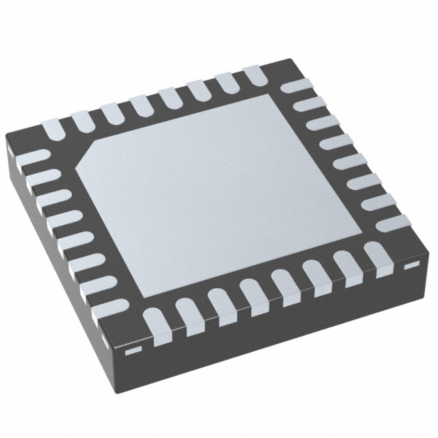


 工商网监
湘ICP备2023018690号
工商网监
湘ICP备2023018690号
