ADS7846
ADS
7846
AD
S784
6
®
AD
S784
6
SBAS125H – SEPTEMBER 1999 – REVISED JANUARY 2005
TOUCH SCREEN CONTROLLER
FEATURES
DESCRIPTION
● SAME PINOUT AS ADS7843
The ADS7846 is a next-generation version to the industry
standard ADS7843 4-wire touch screen controller. The
ADS7846 is 100% pin-compatible with the existing ADS7843,
and drops into the same socket. This allows for easy upgrade
of current applications to the new version. Only software
changes are required to take advantage of the added features of direct battery measurement, temperature measurement, and touch-pressure measurement. The ADS7846 also
has an on-chip 2.5V reference that can be used for the
auxiliary input, battery monitor, and temperature measurement modes. The reference can also be powered down when
not used to conserve power. The internal reference operates
down to 2.7V supply voltage while monitoring the battery
voltage from 0V to 6V.
● 2.2V TO 5.25V OPERATION
● INTERNAL 2.5V REFERENCE
●
●
●
●
DIRECT BATTERY MEASUREMENT (0V to 6V)
ON-CHIP TEMPERATURE MEASUREMENT
TOUCH-PRESSURE MEASUREMENT
QSPITM/SPITM 3-WIRE INTERFACE
● AUTO POWER-DOWN
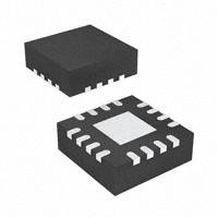
● TSSOP-16, SSOP-16, QFN-16,
AND VFBGA-48 PACKAGES
APPLICATIONS
●
●
●
●
●
●
The low-power consumption of < 0.75mW (typ at 2.7V,
reference off), high speed (up to 125kHz clock rate), and onchip drivers make the ADS7846 an ideal choice for batteryoperated systems such as personal digital assistants (PDAs)
with resistive touch screens, pagers, cellular phones, and
other portable equipment. The ADS7846 is available in the
small TSSOP-16, SSOP-16, QFN-16, and VFBGA-48 packages and is specified over the –40°C to +85°C temperature
range.
PERSONAL DIGITAL ASSISTANTS
PORTABLE INSTRUMENTS
POINT-OF-SALE TERMINALS
PAGERS
TOUCH SCREEN MONITORS
CELLULAR PHONES
US Patent No. 6246394
QSPI and SPI are registered trademarks of Motorola.
PENIRQ
+VCC
X+
Temperature
Sensor
X–
SAR
Y+
ADS7846
DOUT
Y–
BUSY
Comparator
6-Channel
MUX
VBAT
Serial
Data
Out
CDAC
CS
DCLK
Battery
Monitor
DIN
AUX
Internal 2.5V
Reference
VREF
Please be aware that an important notice concerning availability, standard warranty, and use in critical applications of
Texas Instruments semiconductor products and disclaimers thereto appears at the end of this data sheet.
All trademarks are the property of their respective owners.
Copyright © 1999-2005, Texas Instruments Incorporated
PRODUCTION DATA information is current as of publication date.
Products conform to specifications per the terms of Texas Instruments
standard warranty. Production processing does not necessarily include
testing of all parameters.
www.ti.com
�ABSOLUTE MAXIMUM RATINGS(1)
+VCC to GND ........................................................................ –0.3V to +6V
Analog Inputs to GND ............................................ –0.3V to +VCC + 0.3V
Digital Inputs to GND ............................................. –0.3V to +VCC + 0.3V
Power Dissipation .......................................................................... 250mW
Maximum Junction Temperature ................................................... +150°C
Operating Temperature Range ........................................ –40°C to +85°C
Storage Temperature Range ......................................... –65°C to +150°C
Lead Temperature (soldering, 10s) ............................................... +300°C
NOTE: (1) Stresses above these ratings can cause permanent damage.
Exposure to absolute maximum conditions for extended periods may degrade
device reliability.
ELECTROSTATIC
DISCHARGE SENSITIVITY
This integrated circuit can be damaged by ESD. Texas Instruments recommends that all integrated circuits be handled with
appropriate precautions. Failure to observe proper handling
and installation procedures can cause damage.
ESD damage can range from subtle performance degradation
to complete device failure. Precision integrated circuits may be
more susceptible to damage because very small parametric
changes could cause the device not to meet its published
specifications.
PACKAGE/ORDERING INFORMATION(1)
PRODUCT
MAXIMUM
INTEGRAL
LINEARITY
ERROR (LSB)
ADS7846E
PACKAGE-LEAD
PACKAGE
DESIGNATOR
SPECIFIED
TEMPERATURE
RANGE
PACKAGE
MARKING
ORDERING
NUMBER
±2
SSOP-16
DBQ
–40°C to +85°C
ADS7846E
"
"
"
"
"
ADS7846E
ADS7846E/2K5
±2
TSSOP-16
PW
–40°C to +85°C
ADS7846N
"
"
"
"
"
"
"
"
"
"
ADS7846N
ADS7846N/2K5
ADS7846N/2K5G4
ADS7846I
±2
VFBGA-48
GQC
–40°C to +85°C
ADS7846
ADS7846IGQCR
ADS7846I
±2
QFN-16
RGV
–40°C to +85°C
ADS7846
"
"
"
"
"
ADS7846IRGVT
ADS7846IRGVR
"
ADS7846N
"
"
"
NOTE: (1) For the most current package and ordering information, see the Package Option Addendum located at the end of this data sheet, or see the TI web site
at www.ti.com.
2
ADS7846
www.ti.com
SBAS125H
�ELECTRICAL CHARACTERISTICS
At TA = –40°C to +85°C, +VCC = +2.7V, VREF = 2.5V internal voltage, fSAMPLE = 125kHz, fCLK = 16 • fSAMPLE = 2MHz, 12-bit mode, and digital inputs = GND or +VCC,
unless otherwise noted.
ADS7846E
PARAMETER
ANALOG INPUT
Full-Scale Input Span
Absolute Input Range
CONDITIONS
MIN
Positive Input-Negative Input
Positive Input
Negative Input
0
–0.2
–0.2
Capacitance
Leakage Current
SYSTEM PERFORMANCE
Resolution
No Missing Codes
Integral Linearity Error
Offset Error
Gain Error
Noise
Power-Supply Rejection
SAMPLING DYNAMICS
Conversion Time
Acquisition Time
Throughput Rate
Multiplexer Settling Time
Aperture Delay
Aperture Jitter
Channel-to-Channel Isolation
SWITCH DRIVERS
On-Resistance
Y+, X+
Y–, X–
Drive Current(2)
BATTERY MONITOR
Input Voltage Range
Input Impedance
Sampling Battery
Battery Monitor Off
Accuracy
TEMPERATURE MEASUREMENT
Temperature Range
Resolution
Accuracy
DIGITAL INPUT/OUTPUT
Logic Family
Logic Levels, Except PENIRQ
VIH
VIL
VOH
VOL
PENIRQ
VOL
Data Format
POWER-SUPPLY REQUIREMENTS
+VCC(5)
Quiescent Current
Power Dissipation
MAX
UNITS
VREF
+VCC + 0.2
+0.2
V
V
V
pF
µA
25
0.1
12
11
External VREF
Including Internal VREF
±2
±6
±4
70
70
12
3
125
500
30
100
100
VIN = 2.5Vp-p at 50kHz
5
6
Duration 100ms
REFERENCE OUTPUT
Internal Reference Voltage
Internal Reference Drift
Quiescent Current
REFERENCE INPUT
Range
Input Impedance
TYP
50
2.45
2.50
15
500
+VCC
1
V
GΩ
250
Ω
6.0
V
+2
+3
kΩ
GΩ
%
%
10
1
–2
–3
–40
Differential Method(3)
TEMP0(4)
Differential Method(3)
TEMP0(4)
Ω
Ω
mA
V
ppm/°C
µA
0.5
External VREF = 2.5V
Internal Reference
CLK Cycles
CLK Cycles
kHz
ns
ns
ps
dB
2.55
1.0
SER/DFR = 0, PD1 = 0,
Internal Reference Off
Internal Reference On
Bits
Bits
LSB(1)
LSB
LSB
µVrms
dB
+85
1.6
0.3
±2
±3
°C
°C
°C
°C
°C
CMOS
| IIH | ≤ +5µA
| IIL | ≤ +5µA
IOH = –250µA
IOL = 250µA
+VCC • 0.7
–0.3
+VCC • 0.8
+VCC + 0.3
+0.8
TA = 0°C to +85°C, 50kΩ Pull-Up
0.4
V
V
V
0.8
V
3.6
5.25
650
3
V
V
µA
µA
µA
µA
1.8
mW
+85
°C
Straight Binary
Specified Performance
Operating Range
Internal Reference Off
Internal Reference On
fSAMPLE = 12.5kHz
Power-Down Mode with
CS = DCLK = DIN = +VCC
+VCC = +2.7V
TEMPERATURE RANGE
Specified Performance
2.7
2.2
280
780
220
–40
NOTES: (1) LSB means least significant bit. With VREF equal to +2.5V, one LSB is 610µV. (2) Ensured by design, but not tested. Exceeding 50mA source current
may result in device degradation. (3) Difference between TEMP0 and TEMP1 measurement. No calibration necessary. (4) Temperature drift is –2.1mV/°C.
(5) ADS7846 operates down to 2.2V.
ADS7846
SBAS125H
www.ti.com
3
�PIN CONFIGURATION
Top View
Top View
SSOP, TSSOP
VFBGA
CS
DCLK
+VCC
1
16
DCLK
X+
2
15
CS
Y+
3
14
DIN
X–
4
13
BUSY
Y–
5
GND
6
ADS7846
1
2
DIN
3
BUSY DOUT
4
5
6
A NC
7
NC
B
NC
C
NC
NC
NC
NC
NC
NC
NC
NC
PENIRQ
+VCC
12
DOUT
11
PENIRQ
+VCC
+VCC
D
NC
NC
NC
NC
NC
E
NC
NC
NC
NC
NC
F NC
NC
NC
NC
NC
NC
X+
VBAT
7
10
+VCC
AUX
8
9
VREF
VREF
AUX
Y+
G NC
NC
X–
Y–
GND
GND
VBAT
BUSY
1
DIN
2
13 VREF
14 +VCC
15 PENIRQ
QFN
16 DOUT
Top View
NC
12
AUX
11
VBAT
ADS7846
8
Y–
X–
9
7
4
Y+
DCLK
6
GND
X+
10
5
3
+VCC
CS
PIN DESCRIPTION
4
SSOP AND
TSSOP PIN #
VFBGA PIN #
QFN PIN #
NAME
1
2
3
4
5
6
7
8
9
10
11
12
B1 and C1
D1
E1
G2
G3
G4 and G5
G6
E7
D7
C7
B7
A6
5
6
7
8
9
10
11
12
13
14
15
16
+VCC
X+
Y+
X–
Y–
GND
VBAT
AUX
VREF
+VCC
PENIRQ
DOUT
13
14
15
A5
A4
A3
1
2
3
BUSY
DIN
CS
16
A2
4
DCLK
DESCRIPTION
Power Supply
X+ Position Input
Y+ Position Input
X– Position Input
Y– Position Input
Ground
Battery Monitor Input
Auxiliary Input to ADC
Voltage Reference Input/Output
Digital I/O Power Supply
Pen Interrupt. Open anode output (requires 10kΩ to 100kΩ pull-up resistor externally).
Serial Data Output. Data is shifted on the falling edge of DCLK. This output is high
impedance when CS is high.
Busy Output. This output is high impedance when CS is high.
Serial Data Input. If CS is low, data is latched on rising edge of DCLK.
Chip Select Input. Controls conversion timing and enables the serial input/output register.
CS high = power-down mode (ADC only).
External Clock Input. This clock runs the SAR conversion process and synchronizes serial data
I/O.
ADS7846
www.ti.com
SBAS125H
�TYPICAL CHARACTERISTICS
At TA = +25°C, +VCC = +2.7V, VREF = External +2.5V, fSAMPLE = 125kHz, and fCLK = 16 • fSAMPLE = 2MHz, unless otherwise noted.
POWER-DOWN SUPPLY CURRENT
vs TEMPERATURE
400
140
350
120
Supply Current (nA)
Supply Current (µA)
SUPPLY CURRENT vs TEMPERATURE
300
250
200
150
100
80
60
40
100
20
–40
–20
0
20
60
40
80
100
–40
–20
0
20
40
60
80
100
Temperature (°C)
Temperature (°C)
SUPPLY CURRENT vs +VCC
MAXIMUM SAMPLE RATE vs +VCC
1M
390
370
Sample Rate (Hz)
Supply Current (µA)
fSAMPLE = 12.5kHz
350
330
310
290
100k
10k
270
1k
250
2.0
2.5
3.5
3.0
4.0
4.5
2.0
5.0
2.5
3.0
4.0
4.5
5.0
CHANGE IN OFFSET vs TEMPERATURE
CHANGE IN GAIN vs TEMPERATURE
0.15
0.6
0.10
0.4
Delta from +25°C (LSB)
Delta from +25°C (LSB)
3.5
+VCC (V)
+VCC (V)
0.05
0
–0.05
0.2
0
–0.2
–0.4
–0.10
–0.6
–0.15
–40
–20
0
20
40
60
80
100
–20
0
20
40
60
80
100
Temperature (°C)
Temperature (°C)
ADS7846
SBAS125H
–40
www.ti.com
5
�TYPICAL CHARACTERISTICS (Cont.)
At TA = +25°C, +VCC = +2.7V, VREF = External +2.5V, fSAMPLE = 125kHz, and fCLK = 16 • fSAMPLE = 2MHz, unless otherwise noted.
REFERENCE CURRENT vs TEMPERATURE
18
12
16
Reference Current (µA)
Reference Current (µA)
REFERENCE CURRENT vs SAMPLE RATE
14
10
8
6
4
14
12
10
8
2
6
0
0
25
50
75
100
–40
125
–20
0
20
40
60
80
Sample Rate (kHz)
Temperature (°C)
SWITCH-ON RESISTANCE vs +VCC
(X+, Y+: +VCC to Pin; X–, Y–: Pin to GND)
SWITCH-ON RESISTANCE vs TEMPERATURE
(X+, Y+: +VCC to Pin; X–, Y–: Pin to GND)
8
8
7
7
6
6
X–
100
Y–
RON (Ω)
RON (Ω)
Y–
5
X–
4
Y+
X+
5
X+
3
3
2
2
1
1
2.0
2.5
3.0
3.5
4.0
4.5
–40
5.0
0
20
40
60
80
100
INTERNAL VREF vs TEMPERATURE
MAXIMUM SAMPLING RATE vs RIN
2.0
2.4920
1.8
INL: R = 2k
INL: R = 500
DNL: R = 2k
DNL: R = 500
1.4
2.4915
2.4910
Internal VREF (V)
1.6
1.2
1.0
0.8
0.6
2.4905
2.4900
2.4895
2.4890
0.4
2.4885
0.2
2.4880
0
2.4875
20
40
60
80
100 120 140
Sampling Rate (kHz)
160
180
–40
–35
–30
–25
–20
–15
–10
–05
0
05
10
15
20
25
30
35
40
45
50
55
60
65
70
75
80
85
Error (LSB)
–20
Temperature (°C)
+VCC (V)
6
Y+
4
200
Temperature (°C)
ADS7846
www.ti.com
SBAS125H
�TYPICAL CHARACTERISTICS (Cont.)
At TA = +25°C, +VCC = +2.7V, VREF = External +2.5V, fSAMPLE = 125kHz, and fCLK = 16 • fSAMPLE = 2MHz, unless otherwise noted.
INTERNAL VREF vs TURN-ON TIME
2.4860
80
Internal VREF (%)
100
2.4855
2.4850
3.6
3.5
3.4
3.3
3.2
3.1
3.0
2.9
2.8
0
2.7
2.4840
0
200
400
600
800
1000
1200
Turn-On Time (µS)
VCC (V)
TEMP DIODE VOLTAGE
vs TEMPERATURE (2.7V SUPPLY)
TEMP0 DIODE VOLTAGE vs VSUPPLY (25°C)
620
850
750
TEMP0 Diode Voltage (mV)
800
TEMP Diode Voltage (mV)
1µF Cap
(1110µS)
12-Bit
Settling
40
20
2.6
No Cap
(52µS)
12-Bit
Settling
60
2.4845
2.5
VREF (V)
INTERNAL VREF vs VCC
2.4865
TEMP1
102.7mV
700
650
132.25mV
600
TEMP0
550
618
616
614
612
500
610
450
3.0
–40
–35
–30
–25
–20
–15
–10
–05
0
05
10
15
20
25
30
35
40
45
50
55
60
65
70
75
80
85
2.7
3.3
VSUPPLY (V)
Temperature (°C)
TEMP1 DIODE VOLTAGE vs VSUPPLY (25°C)
TEMP1 Diode Voltage (mV)
732
730
728
726
724
722
2.7
3.0
3.3
VSUPPLY (V)
ADS7846
SBAS125H
www.ti.com
7
�THEORY OF OPERATION
possible to negate the error from each touch panel driver
switch’s on-resistance (if this is a source of error for the
particular measurement).
The ADS7846 is a classic successive approximation register
(SAR) analog-to-digital converter (ADC). The architecture is
based on capacitive redistribution which inherently includes
a sample-and-hold function. The converter is fabricated on a
0.6µm CMOS process.
ANALOG INPUT
See Figure 2 for a block diagram of the input multiplexer on
the ADS7846, the differential input of the ADC, and the
differential reference of the converter. Table I and Table II
show the relationship between the A2, A1, A0, and SER/DFR
control bits and the configuration of the ADS7846. The
control bits are provided serially via the DIN pin—see the
Digital Interface section of this data sheet for more details.
The basic operation of the ADS7846 is shown in Figure 1.
The device features an internal 2.5V reference and an
external clock. Operation is maintained from a single supply
of 2.7V to 5.25V. The internal reference can be overdriven
with an external, low impedance source between 1V and
+VCC. The value of the reference voltage directly sets the
input range of the converter.
When the converter enters the hold mode, the voltage
difference between the +IN and –IN inputs (see Figure 2) is
captured on the internal capacitor array. The input current
into the analog inputs depends on the conversion rate of the
device. During the sample period, the source must charge
the internal sampling capacitor (typically 25pF). After the
capacitor has been fully charged, there is no further input
current. The rate of charge transfer from the analog source
to the converter is a function of conversion rate.
The analog input (X-, Y-, and Z-position coordinates, auxiliary input, battery voltage, and chip temperature) to the
converter is provided via a multiplexer. A unique configuration of low on-resistance touch panel driver switches allows
an unselected ADC input channel to provide power and its
accompanying pin to provide ground for an external device,
such as a touch screen. By maintaining a differential input to
the converter and a differential reference architecture, it is
+2.7V to +5V
1µF
+
to
10µF
(Optional)
ADS7846
0.1µF
Touch
Screen
To Battery
Auxiliary Input
Serial/Conversion Clock
1
+VCC
DCLK 16
2
X+
CS 15
3
Y+
DIN 14
4
X–
BUSY 13
Converter Status
5
Y–
DOUT 12
Serial Data Out
6
GND
PENIRQ 11
7
VBAT
+VCC 10
8
AUX
VREF
Chip Select
Serial Data In
Pen Interrupt
50kΩ
9
Voltage
Regulator
FIGURE 1. Basic Operation of the ADS7846.
A2
A1
A0
0
0
0
0
1
1
1
1
0
0
1
1
0
0
1
1
0
1
0
1
0
1
0
1
VBAT
AUXIN
TEMP
Y–
X+
Y+
Y-POSITION
X-POSITION
Z1-POSITION Z2-POSITION
+IN (TEMP0)
+IN
Measure
+IN
+IN
Measure
+IN
Measure
+IN
Measure
+IN
+IN (TEMP1)
X-DRIVERS
Y-DRIVERS
Off
Off
Off
X–, On
X–, On
On
Off
Off
Off
On
Off
Y+, On
Y+, On
Off
Off
Off
TABLE I. Input Configuration (DIN), Single-Ended Reference Mode (SER/DFR high).
A2
A1
A0
+REF
–REF
0
0
1
1
0
1
0
0
1
1
0
1
Y+
Y+
Y+
X+
Y–
X–
X–
X–
Y–
X+
Y+
+IN
+IN
Y-POSITION
X-POSITION
Z1-POSITION
Z2-POSITION
Measure
Measure
+IN
Measure
+IN
Measure
DRIVERS ON
Y+,
Y+,
Y+,
X+,
Y–
X–
X–
X–
TABLE II. Input Configuration (DIN), Differential Reference Mode (SER/DFR low).
8
ADS7846
www.ti.com
SBAS125H
�+VCC
PENIRQ
TEMP1
VREF
TEMP0
A2-A0
(Shown 001B)
SER/DFR
(Shown High)
X+
X–
Ref On/Off
Y+
+IN
Y–
+REF
Converter
2.5V
Reference
–IN
–REF
7.5kΩ
VBAT
2.5kΩ
AUX
Battery
On
GND
FIGURE 2. Simplified Diagram of Analog Input.
INTERNAL REFERENCE
Reference
Power Down
The ADS7846 has an internal 2.5V voltage reference that can
be turned on or off with the control bit, PD1 = 1 (see Table V and
Figure 3). Typically, the internal reference voltage is only used
in the single-ended mode for battery monitoring, temperature
measurement, and for using the auxiliary input. Optimal touch
screen performance is achieved when using the differential
mode. The internal reference voltage of the ADS7846 must be
commanded to be off to maintain compatibility with the ADS7843.
Therefore, after power-up, a write of PD1 = 0 is required to
insure the reference is off (see the Typical Characteristics for
power-up time of the reference from power-down).
Band
Gap
VREF
Buffer
To
CDAC
Optional
FIGURE 3. Simplified Diagram of the Internal Reference.
REFERENCE INPUT
The voltage difference between +REF and –REF (shown in
Figure 2) sets the analog input range. The ADS7846 operates with a reference in the range of 1V to +VCC. There are
several critical items concerning the reference input and its
wide voltage range. As the reference voltage is reduced, the
analog voltage weight of each digital output code is also
reduced. This is often referred to as the LSB (least significant
bit) size and is equal to the reference voltage divided by 4096
in 12-bit mode. Any offset or gain error inherent in the ADC
appears to increase, in terms of LSB size, as the reference
voltage is reduced. For example, if the offset of a given
converter is 2LSBs with a 2.5V reference, it is typically
5LSBs with a 1V reference. In each case, the actual offset of
the device is the same, 1.22mV. With a lower reference
ADS7846
SBAS125H
www.ti.com
9
�voltage, more care must be taken to provide a clean layout
including adequate bypassing, a clean (low-noise, low-ripple)
power supply, a low-noise reference (if an external reference
is used), and a low-noise input signal.
+VCC
The voltage into the VREF input directly drives the capacitor
digital-to-analog converter (CDAC) portion of the ADS7846.
Therefore, the input current is very low (typically < 13µA).
There is also a critical item regarding the reference when
making measurements where the switch drivers are on. For
this discussion, it is useful to consider the basic operation of
the ADS7846 (see Figure 1). This particular application
shows the device being used to digitize a resistive touch
screen. A measurement of the current Y position of the
pointing device is made by connecting the X+ input to the
ADC, turning on the Y+ and Y– drivers, and digitizing the
voltage on X+ (Figure 4 shows a block diagram). For this
measurement, the resistance in the X+ lead does not affect
the conversion (it does affect the settling time, but the
resistance is usually small enough that this is not a concern).
However, since the resistance between Y+ and Y– is fairly
low, the on-resistance of the Y drivers does make a small
difference. Under the situation outlined so far, it is not
possible to achieve a 0V input or a full-scale input regardless
of where the pointing device is on the touch screen, because
some voltage is lost across the internal switches. In addition,
the internal switch resistance is unlikely to track the resistance of the touch screen, providing an additional source of error.
+VCC
VREF
Y+
X+
+IN
+REF
Converter
–IN
–REF
Y–
GND
FIGURE 5. Simplified Diagram of Differential Reference
(SER/DFR Low, Y Switches Enabled, X+ is
Analog Input).
As a final note about the differential reference mode, it must
be used with +VCC as the source of the +REF voltage and
cannot be used with VREF. It is possible to use a high
precision reference on VREF and single-ended reference
mode for measurements which do not need to be ratiometric.
In some cases, it is possible to power the converter directly
from a precision reference. Most references can provide
enough power for the ADS7846, but might not be able to
supply enough current for the external load (such as a
resistive touch screen).
TOUCH SCREEN SETTLING
Y+
X+
+IN
+REF
Converter
–IN
–REF
Y–
GND
FIGURE 4. Simplified Diagram of Single-Ended Reference
(SER/DFR High, Y Switches Enabled, X+ is
Analog Input).
This situation can be remedied as shown in Figure 5. By
setting the SER/DFR bit low, the +REF and –REF inputs are
connected directly to Y+ and Y–, respectively, which makes
the analog-to-digital conversion ratiometric. The result of the
conversion is always a percentage of the external resistance,
regardless of how it changes in relation to the on-resistance of
the internal switches. Note that there is an important consideration regarding power dissipation when using the ratiometric
mode of operation (see the Power Dissipation section for
more details).
10
In some applications, external capacitors may be required
across the touch screen for filtering noise picked up by the
touch screen (for example, noise generated by the LCD panel
or backlight circuitry). These capacitors provide a low-pass
filter to reduce the noise, but cause a settling time requirement
when the panel is touched that typically shows up as a gain
error. The problem is that the input and/or reference has not
settled to the final steady-state value prior to the ADC sampling the input(s) and providing the digital output. Additionally,
the reference voltage may still be changing during the measurement cycle. There are several methods for minimizing or
eliminating this issue. Option 1 is to stop or slow down the
ADS7846 DCLK for the required touch screen settling time.
This allows the input and reference to have stable values for
the Acquire period (3 clock cycles of the ADS7846; see Figure
9). This works for both the single-ended and the differential
modes. Option 2 is to operate the ADS7846 in the differential
mode only for the touch screen measurements and command
the ADS7846 to remain on (touch screen drivers on) and not
go into power-down (PD0 = 1). Several conversions are made
depending on the settling time required and the ADS7846 data
rate. Once the required number of conversions have been
made, the processor commands the ADS7846 to go into the
power-down state on the last measurement. This process is
ADS7846
www.ti.com
SBAS125H
�required for X-position, Y-position, and Z-position measurements. Option 3 is to operate in the 15 Clock-per-Conversion
mode which overlaps the analog-to-digital conversions and
maintains the touch screen drivers on until commanded to
stop by the processor (see Figure 12).
TEMPERATURE MEASUREMENT
In some applications, such as battery recharging, a measurement of ambient temperature is required. The temperature
measurement technique used in the ADS7846 relies on the
characteristics of a semiconductor junction operating at a
fixed current level. The forward diode voltage (VBE) has a
well-defined characteristic versus temperature. The ambient
temperature can be predicted in applications by knowing the
25°C value of the VBE voltage and then monitoring the delta
of that voltage as the temperature changes. The ADS7846
offers two modes of operation. The first mode requires
calibration at a known temperature, but only requires a single
reading to predict the ambient temperature. The PENIRQ
diode is used (turned on) during this measurement cycle.
The voltage across the diode is connected through the MUX
for digitizing the forward bias voltage by the ADC with an
address of A2 = 0, A1 = 0, and A0 = 0 (see Table I and Figure
6 for details). This voltage is typically 600mV at +25°C with
a 20µA current through the diode. The absolute value of this
diode voltage can vary a few millivolts. However, the TC of
this voltage is very consistent at –2.1mV/°C. During the final
test of the end product, the diode voltage would be stored at
a known room temperature, in memory, for calibration purposes by the user. The result is an equivalent temperature
measurement resolution of 0.3°C/LSB (in 12-bit mode).
represented by kT/q • ln (N), where N is the current ratio
= 91, k = Boltzmann’s constant (1.38054 • 10–23 electron
volts/degrees Kelvin), q = the electron charge (1.602189 •
10–19 C), and T = the temperature in degrees Kelvin. This
method can provide improved absolute temperature measurement over the first mode at the cost of less resolution
(1.6°C/LSB). The equation for solving for °K is:
°K = q • ∆V/(k • ln (N))
where,
(1)
∆V = V (I91) – V (I1) (in mV)
∴ °K = 2.573°K/mV • ∆V
°C = 2.573 • ∆V(mV) – 273°K
NOTE: The bias current for each diode temperature measurement is only on for 3 clock cycles (during the acquisition
mode). Therefore, it does not add any noticeable increase in
power, especially if the temperature measurement only occurs occasionally.
BATTERY MEASUREMENT
An added feature of the ADS7846 is the ability to monitor the
battery voltage on the other side of the voltage regulator (DC/DC
converter), as shown in Figure 7. The battery voltage can vary
from 0.5V to 6V, while maintaining the voltage to the ADS7846
at 2.7V, 3.3V, etc. The input voltage (VBAT) is divided down by
4 so that a 6.0V battery voltage is represented as 1.5V to the
ADC. This simplifies the multiplexer and control logic. In order
to minimize the power consumption, the divider is only on
during the sampling period when A2 = 0, A1 = 1, and A0 = 0
(see Table I for the relationship between the control bits and
configuration of the ADS7846).
+VCC
External
Pull-Up
PENIRQ
2.7V
DC/DC
Converter
X+
MUX
Battery
0.5V +
to
6.0V
ADC
+VCC
Temperature Select
TEMP0
0.125V to 1.5V
VBAT
TEMP1
7.5kΩ
FIGURE 6. Functional Block Diagram of Temperature Measurement Mode.
The second mode does not require a test temperature
calibration, but uses a two-measurement method to eliminate
the need for absolute temperature calibration and for achieving 2°C accuracy. This mode requires a second conversion
with an address of A2 = 1, A1 = 1, and A0 = 1, with a 91 times
larger current. The voltage difference between the first
and second conversion using 91 times the bias current is
2.5kΩ
FIGURE 7. Battery Measurement Functional Block Diagram.
ADS7846
SBAS125H
www.ti.com
11
�PRESSURE MEASUREMENT
Measure X-Position
Measuring touch pressure can also be done with the ADS7846.
To determine pen or finger touch, the pressure of the touch
needs to be determined. Generally, it is not necessary to have
very high performance for this test; therefore, the 8-bit resolution mode is recommended (however, calculations will be
shown here are in 12-bit resolution mode). There are several
different ways of performing this measurement. The ADS7846
supports two methods. The first method requires knowing the
X-plate resistance, measurement of the X-Position, and two
additional cross-panel measurements (Z1 and Z2) of the touch
screen, as shown in Figure 8. Using Equation 2 calculates the
touch resistance:
RTOUCH = RX – plate •
X – Position Z2
– 1
4096
Z1
X+
Touch
X-Position
Y–
X–
Measure Z1-Position
Y+
X+
Touch
Z1-Position
(2)
X–
The second method requires knowing both the X-plate and
Y-plate resistance, measurement of X-Position and Y-Position, and Z1. Using Equation 3 also calculates the touch
resistance:
R TOUCH =
Y+
Y–
Y+
X+
Touch
R X − plate • X − Position 4096
Z – 1
4096
1
Z2-Position
(3)
Y Position
– R Y − plate • 1–
4096
X–
Y–
Measure Z2-Position
DIGITAL INTERFACE
FIGURE 8. Pressure Measurement Block Diagrams.
Figure 9 shows the typical operation of the ADS7846 digital
interface. This diagram assumes that the source of the
digital signals is a microcontroller or digital signal processor
with a basic serial interface. Each communication between
the processor and the converter, such as SPI/SSI or
Microwire™ synchronous serial interface, consists of eight
clock cycles. One complete conversion can be accomplished with three serial communications for a total of 24
clock cycles on the DCLK input.
The first eight clock cycles are used to provide the control
byte via the DIN pin. When the converter has enough
information about the following conversion to set the input
multiplexer and reference inputs appropriately, the converter
enters the acquisition (sample) mode and, if needed,
the touch panel drivers are turned on. After three more
clock cycles, the control byte is complete and the converter
enters the conversion mode. At this point, the input
CS
tACQ
DCLK
DIN
1
S
8
A2
A1
8
1
1
8
SER/
A0 MODE DFR PD1 PD0
(START)
Idle
Acquire
Conversion
Idle
BUSY
DOUT
11
10
9
8
7
6
5
4
3
(MSB)
DRIVERS 1 AND 2(1)
(SER/DFR High)
DRIVERS 1 AND 2(1, 2)
(SER/DFR Low)
Off
2
1
0
Zero Filled...
(LSB)
On
Off
Off
On
Off
NOTES: (1) For Y-Position, Driver 1 is on, X+ is selected, and Driver 2 is off. For X-Position, Driver 1 is off, Y+ is selected, and
Driver 2 is on. Y– will turn on when power-down mode is entered and PD0 = 0B. (2) Drivers will remain on if PD0 = 1 (no power
down) until selected input channel, reference mode, or power-down mode is changed, or CS is HIGH.
FIGURE 9. Conversion Timing, 24 Clocks-per-Conversion, 8-bit Bus Interface. No DCLK delay required with dedicated
serial port.
12
ADS7846
www.ti.com
SBAS125H
�sample-and-hold goes into the hold mode and the touch
panel drivers turn off (in single-ended mode). The next 12
clock cycles accomplish the actual analog-to-digital conversion. If the conversion is ratiometric (SER/DFR = 0), the
drivers are on during the conversion and a 13th clock cycle
is needed for the last bit of the conversion result. Three more
clock cycles are needed to complete the last byte (DOUT will
be low), which are ignored by the converter.
Control Byte
The control byte (on DIN), as shown in Table III, provides the
start conversion, addressing, ADC resolution, configuration,
and power-down of the ADS7846. Figure 9 and Tables III
and IV give detailed information regarding the order and
description of these control bits within the control byte.
Bit 7
(MSB)
Bit 6
Bit 5
Bit 4
S
A2
A1
A0
Bit 3
Bit 2
MODE SER/DFR
Bit 1
Bit 0
(LSB)
PD1
PD0
TABLE III. Order of the Control Bits in the Control Byte.
BIT
NAME
7
S
DESCRIPTION
Start Bit. Control byte starts with first high bit on DIN.
A new control byte can start every 15th clock cycle
in 12-bit conversion mode or every 11th clock cycle
in 8-bit conversion mode (see Figure 12).
6-4
A2-A0
Channel Select Bits. Along with the SER/DFR bit,
these bits control the setting of the multiplexer input,
touch driver switches, and reference inputs (see
Tables I and II).
3
MODE
12-Bit/8-Bit Conversion Select Bit. This bit controls
the number of bits for the next conversion: 12-bits
(low) or 8-bits (high).
2
SER/DFR
Single-Ended/Differential Reference Select Bit. Along
with bits A2-A0, this bit controls the setting of the
multiplexer input, touch driver switches, and reference
inputs (see Tables I and I).
1-0
PD1-PD0
Power-Down Mode Select Bits. See Table V for
details.
TABLE IV. Descriptions of the Control Bits within the Control
Byte.
SER/DFR—The SER/DFR bit controls the reference mode,
either single-ended (high) or differential (low). The differential
mode is also referred to as the ratiometric conversion mode
and is preferred for X-Position, Y-Position, and PressureTouch measurements for optimum performance. The reference is derived from the voltage at the switch drivers, which
is almost the same as the voltage to the touch screen. In this
case a reference voltage is not needed, as the reference
voltage to the ADC is the voltage across the touch screen. In
the single-ended mode, the converter reference voltage is
always the difference between the VREF and GND pins (see
Tables I and II, and Figures 2 through 5 for further information).
If X-Position, Y-Position, and Pressure-Touch are measured
in the single-ended mode, an external reference voltage is
needed. The ADS7846 should also be powered from the
external reference. Caution must be observed when using
the single-ended mode such that the input voltage to the
ADC does not exceed the internal reference voltage, especially if the supply voltage is greater than 2.7V.
NOTE: The differential mode can only be used for X-Position,
Y-Position, and Pressure-Touch measurements. All other
measurements require the single-ended mode.
PD0 and PD1—Table V describes the power-down and the
internal reference voltage configurations. The internal reference voltage can be turned on or off independently of the
ADC. This can allow extra time for the internal reference
voltage to settle to the final value prior to making a conversion. Make sure to also allow this extra wake-up time if the
internal reference is powered down. The ADC requires no
wake-up time and can be instantaneously used. Also note
that the status of the internal reference power-down is
latched into the part (internally) with BUSY going high.
Therefore, in order to turn the reference off, an additional
write to the ADS7846 is required after the channel is converted.
PD1
PD0
PENIRQ
DESCRIPTION
0
0
Enabled
Power-Down Between Conversions. When each
conversion is finished, the converter enters a
low-power mode. At the start of the next conversion, the device instantly powers up to full power.
There is no need for additional delays to assure
full operation and the very first conversion is
valid. The Y– switch is on when in power-down.
0
1
Disabled
Reference is off and ADC is on.
1
0
Enabled
Reference is on and ADC is off.
1
1
Disabled
Device is always powered. Reference is on and
ADC is on.
Initiate START—The first bit, the S bit, must always be high
and initiates the start of the control byte. The ADS7846
ignores inputs on the DIN pin until the start bit is detected.
Addressing—The next three bits (A2, A1, and A0) select the
active input channel(s) of the input multiplexer (see Tables I,
II, and Figure 2), touch screen drivers, and the reference
inputs.
MODE—The mode bit sets the resolution of the ADC. With
this bit low, the next conversion has 12 bits of resolution; with
this bit high, the next conversion has 8 bits of resolution.
TABLE V. Power-Down and Internal Reference Selection.
ADS7846
SBAS125H
www.ti.com
13
�16 Clocks-per-Conversion
SYMBOL
DESCRIPTION
MIN
The control bits for conversion n + 1 can be overlapped with
conversion n to allow for a conversion every 16 clock cycles,
as shown in Figure 10. This figure also shows possible serial
communication occurring with other serial peripherals between each byte transfer from the processor to the converter.
This is possible provided that each conversion completes
within 1.6ms of starting. Otherwise, the signal that is captured on the input sample-and-hold may droop enough to
affect the conversion result. Note that the ADS7846 is fully
powered while other serial communications are taking place
during a conversion.
tACQ
Acquisition Time
1.5
tDS
DIN Valid Prior to DCLK Rising
100
ns
tDH
DIN Hold After DCLK High
10
ns
Digital Timing
Figures 9, 11, and Table VI provide detailed timing for the
digital interface of the ADS7846.
TYP
MAX
UNITS
µs
tDO
DCLK Falling to DOUT Valid
200
ns
tDV
CS Falling to DOUT Enabled
200
ns
200
ns
tTR
CS Rising to DOUT Disabled
tCSS
CS Falling to First DCLK Rising
100
tCSH
CS Rising to DCLK Ignored
0
ns
tCH
DCLK High
200
ns
tCL
DCLK Low
200
tBD
DCLK Falling to BUSY Rising
200
ns
tBDV
CS Falling to BUSY Enabled
200
ns
tBTR
CS Rising to BUSY Disabled
200
ns
ns
ns
TABLE VI. Timing Specifications (+VCC = +2.7V and Above,
TA = –40°C to +85°C, CLOAD = 50pF).
CS
DCLK
1
DIN
8
1
8
1
S
8
1
S
Control Bits
Control Bits
BUSY
DOUT
11 10 9
8
7
6
5
4
3
2
1
0
11 10 9
FIGURE 10. Conversion Timing, 16 Clocks-per-Conversion, 8-Bit Bus Interface. No DCLK delay required with dedicated
serial port.
CS
tCSS
tCL
tCH
tBD
tBD
tD0
tCSH
DCLK
tDS
tDH
PD0
DIN
tBDV
tBTR
BUSY
tDV
tTR
DOUT
11
10
FIGURE 11. Detailed Timing Diagram.
14
ADS7846
www.ti.com
SBAS125H
�15 Clocks-per-Conversion
8-Bit Conversion
Figure 12 provides the fastest way to clock the ADS7846.
This method does not work with the serial interface of most
microcontrollers and digital signal processors, as they are
generally not capable of providing 15 clock cycles per serial
transfer. However, this method can be used with field programmable gate arrays (FPGAs) or application specific integrated circuits (ASICs). Note that this effectively increases
the maximum conversion rate of the converter beyond the
values given in the specification tables, which assume 16
clock cycles per conversion.
The ADS7846 provides an 8-bit conversion mode that can be
used when faster throughput is needed and the digital result
is not as critical. By switching to the 8-bit mode, a conversion
is complete four clock cycles earlier. Not only does this shorten
each conversion by four bits (25% faster throughput), but each
conversion can actually occur at a faster clock rate. This is
because the internal settling time of the ADS7846 is not as
critical—settling to better than 8 bits is all that is needed. The
clock rate can be as much as 50% faster. The faster clock rate
and fewer clock cycles combine to provide a 2x increase in
conversion rate.
Data Format
The ADS7846 output data is in Straight Binary format as
shown in Figure 13. This figure shows the ideal output code
for the given input voltage and does not include the effects
of offset, gain, or noise.
POWER DISSIPATION
There are two major power modes for the ADS7846: full power
(PD0 = 1B) and auto power-down (PD0 = 0B). When operating
at full speed and 16 clocks-per-conversion (see Figure 10), the
ADS7846 spends most of the time acquiring or converting.
There is little time for auto power-down, assuming that this
mode is active. Therefore, the difference between full-power
mode and auto power-down is negligible. If the conversion
rate is decreased by slowing the frequency of the DCLK input,
the two modes remain approximately equal. However, if the
DCLK frequency is kept at the maximum rate during a conversion but conversions are done less often, the difference
between the two modes is dramatic.
FS = Full-Scale Voltage = VREF(1)
1LSB = VREF(1)/4096
1LSB
11...111
Output Code
11...110
11...101
00...010
00...001
00...000
FS – 1LSB
0V
Input Voltage(2) (V)
NOTES: (1) Reference voltage at converter: +REF – (–REF), see Figure 2.
(2) Input voltage at converter, after multiplexer: +IN – (–IN), see Figure 2.
FIGURE 13. Ideal Input Voltages and Output Codes.
CS
Power Down
DCLK
15
1
DIN
S
SGL/
A2 A1 A0 MODE DIF PD1 PD0
1
S
15
SGL/
A2 A1 A0 MODE DIF PD1 PD0
1
S
A2
A1 A0
BUSY
DOUT
11 10
9
8
7
6
5
4
3
2
1
0
11 10
9
8
7
Tri-State
FIGURE 12. Maximum Conversion Rate, 15 Clocks-per-Conversion.
ADS7846
SBAS125H
www.ti.com
15
�Figure 14 shows the difference between reducing the DCLK
frequency (scaling DCLK to match the conversion rate) or
maintaining DCLK at the highest frequency and reducing the
number of conversions per second. In the latter case, the
converter spends an increasing percentage of time in powerdown mode (assuming the auto power-down mode is active).
1000
Supply Current (µA)
fCLK = 16 • fSAMPLE
100
fCLK = 2MHz
10
TA = 25°C
+VCC = +2.7V
1
1k
10k
100k
1M
fSAMPLE (Hz)
FIGURE 14. Supply Current versus Directly Scaling the Frequency of DCLK with Sample Rate or Maintaining DCLK at the Maximum Possible Frequency.
Another important consideration for power dissipation is the
reference mode of the converter. In the single-ended reference mode, the touch panel drivers are on only when the
analog input voltage is being acquired (see Figure 9 and
Table I). Therefore, the external device (e.g., a resistive
touch screen) is only powered during the acquisition period.
In the differential reference mode, the external device must
be powered throughout the acquisition and conversion periods (see Figure 9). If the conversion rate is high, this could
substantially increase power dissipation.
CS also puts the ADS7846 into power-down mode. When
CS goes high, the ADS7846 immediately goes into powerdown and does not complete the current conversion. However, the internal reference does not turn off with CS going
high. To turn the reference off, an additional write is required
before CS goes high (PD1 = 0).
16
LAYOUT
The following layout suggestions provide the most optimum
performance from the ADS7846. However, many portable
applications have conflicting requirements concerning power,
cost, size, and weight. In general, most portable devices
have fairly clean power and grounds because most of the
internal components are very low power. This situation means
less bypassing for the converter power and less concern
regarding grounding. Still, each situation is unique and the
following suggestions should be reviewed carefully.
For optimum performance, care must be taken with the
physical layout of the ADS7846 circuitry. The basic SAR
architecture is sensitive to glitches or sudden changes on the
power supply, reference, ground connections, and digital
inputs that occur just prior to latching the output of the analog
comparator. Therefore, during any single conversion for an
n-bit SAR converter, there are n ‘windows’ in which large
external transient voltages can easily affect the conversion
result. Such glitches can originate from switching power
supplies, nearby digital logic, and high-power devices. The
degree of error in the digital output depends on the reference
voltage, layout, and the exact timing of the external event.
The error can change if the external event changes in time
with respect to the DCLK input.
With this in mind, power to the ADS7846 should be clean and
well bypassed. A 0.1µF ceramic bypass capacitor should be
placed as close to the device as possible. A 1µF to 10µF
capacitor may also be needed if the impedance of the
connection between +VCC and the power supply is high. Lowleakage capacitors should be used to minimize power dissipation through the bypass capacitors when the ADS7846 is
in power-down mode.
A bypass capacitor is generally not needed on the VREF pin
because the internal reference is buffered by an internal op
amp. If an external reference voltage originates from an op
amp, make sure that it can drive any bypass capacitor that
is used without oscillation.
The ADS7846 architecture offers no inherent rejection of
noise or voltage variation in regards to using an external
reference input. This is of particular concern when the
reference input is tied to the power supply. Any noise and
ripple from the supply appears directly in the digital results.
Whereas high-frequency noise can be filtered out, voltage
variation due to line frequency (50Hz or 60Hz) can be difficult
to remove.
ADS7846
www.ti.com
SBAS125H
�The GND pin must be connected to a clean ground point. In
many cases, this is the analog ground. Avoid connections
which are too near the grounding point of a microcontroller or
digital signal processor. If needed, run a ground trace directly
from the converter to the power-supply entry or batteryconnection point. The ideal layout includes an analog ground
plane dedicated to the converter and associated analog
circuitry.
+VCC
100kΩ
Y+
In the specific case of use with a resistive touch screen, care
should be taken with the connection between the converter
and the touch screen. Although resistive touch screens have
fairly low resistance, the interconnection should be as short
and robust as possible. Longer connections are a source of
error, much like the on-resistance of the internal switches.
Likewise, loose connections can be a source of error when
the contact resistance changes with flexing or vibrations.
As indicated previously, noise can be a major source of error
in touch screen applications (for example, applications that
require a backlit LCD panel). This EMI noise can be coupled
through the LCD panel to the touch screen and cause
“flickering” of the converted data. Several things can be done
to reduce this error, such as using a touch screen with a
bottom-side metal layer connected to ground to shunt the
majority of noise to ground. Additionally, filtering capacitors,
from Y+, Y–, X+, and X– pins to ground can also help.
Caution should be observed under these circumstances for
settling time of the touch screen, especially operating in the
single-ended mode and at high data rates.
PENIRQ OUTPUT
The pen-interrupt output function is shown in Figure 15. While
in power-down mode with PD0 = 0, the Y– driver is on and
connects the Y-plane of the touch screen to GND. The
PENIRQ output is connected to the X+ input through two
transmission gates. When the screen is touched, the X+ input
is pulled to ground through the touch screen. The PENIRQ
output goes low due to the current path through the touch
screen to ground, which initiates an interrupt to the processor.
During the measurement cycle for X-, Y-, and Z-Position, the
X+ input is disconnected from the external pull-up resistor.
This is done to eliminate any leakage current from the
external pull-up resistor through the touch screen, thus causing no errors.
X+
Y–
On
Y or X drivers on,
or TEMP0, TEMP1
measurements
activated.
FIGURE 15. ADS7846 PENIRQ Functional Block Diagram.
Furthermore, the PENIRQ output is disabled and low during
the measurement cycle for X-, Y-, and Z-Position. The PENIRQ
output is disabled and high during the measurement cycle for
battery monitor, auxiliary input, and chip temperature. If the last
control byte written to the ADS7846 contains PD0 = 1, the peninterrupt output function is disabled and is not able to detect
when the screen is touched. In order to re-enable the peninterrupt output function under these circumstances, a control
byte needs to be written to the ADS7846 with PD0 = 0. If the
last control byte written to the ADS7846 contains PD0 = 0, the
pen-interrupt output function is enabled at the end of the
conversion. The end of the conversion occurs on the falling
edge of DCLK after bit 1 of the converted data is clocked out
of the ADS7846.
It is recommended that the processor mask the interrupt
PENIRQ is associated with whenever the processor sends a
control byte to the ADS7846. This prevents false triggering
of interrupts when the PENIRQ output is disabled, as in the
cases discussed in this section.
ADS7846
SBAS125H
PENIRQ
www.ti.com
17
�PACKAGE OPTION ADDENDUM
www.ti.com
10-Dec-2020
PACKAGING INFORMATION
Orderable Device
Status
(1)
Package Type Package Pins Package
Drawing
Qty
Eco Plan
(2)
Lead finish/
Ball material
MSL Peak Temp
Op Temp (°C)
Device Marking
(3)
(4/5)
(6)
ADS7846E
ACTIVE
SSOP
DBQ
16
75
RoHS & Green
NIPDAU
Level-2-260C-1 YEAR
-40 to 85
ADS
7846E
ADS7846E/2K5
ACTIVE
SSOP
DBQ
16
2500
RoHS & Green
NIPDAU
Level-2-260C-1 YEAR
-40 to 85
ADS
7846E
ADS7846EG4
ACTIVE
SSOP
DBQ
16
75
RoHS & Green
NIPDAU
Level-2-260C-1 YEAR
-40 to 85
ADS
7846E
ADS7846IRGVT
ACTIVE
VQFN
RGV
16
250
RoHS & Green
NIPDAU
Level-2-260C-1 YEAR
-40 to 85
ADS
7846
ADS7846N
ACTIVE
TSSOP
PW
16
90
RoHS & Green
NIPDAU
Level-2-260C-1 YEAR
-40 to 85
ADS
7846N
ADS7846N/2K5
ACTIVE
TSSOP
PW
16
2500
RoHS & Green
NIPDAU
Level-2-260C-1 YEAR
-40 to 85
ADS
7846N
ADS7846N/2K5G4
ACTIVE
TSSOP
PW
16
2500
RoHS & Green
NIPDAU
Level-2-260C-1 YEAR
-40 to 85
ADS
7846N
ADS7846NG4
ACTIVE
TSSOP
PW
16
90
RoHS & Green
NIPDAU
Level-2-260C-1 YEAR
-40 to 85
ADS
7846N
(1)
The marketing status values are defined as follows:
ACTIVE: Product device recommended for new designs.
LIFEBUY: TI has announced that the device will be discontinued, and a lifetime-buy period is in effect.
NRND: Not recommended for new designs. Device is in production to support existing customers, but TI does not recommend using this part in a new design.
PREVIEW: Device has been announced but is not in production. Samples may or may not be available.
OBSOLETE: TI has discontinued the production of the device.
(2)
RoHS: TI defines "RoHS" to mean semiconductor products that are compliant with the current EU RoHS requirements for all 10 RoHS substances, including the requirement that RoHS substance
do not exceed 0.1% by weight in homogeneous materials. Where designed to be soldered at high temperatures, "RoHS" products are suitable for use in specified lead-free processes. TI may
reference these types of products as "Pb-Free".
RoHS Exempt: TI defines "RoHS Exempt" to mean products that contain lead but are compliant with EU RoHS pursuant to a specific EU RoHS exemption.
Green: TI defines "Green" to mean the content of Chlorine (Cl) and Bromine (Br) based flame retardants meet JS709B low halogen requirements of


 工商网监
湘ICP备2023018690号
工商网监
湘ICP备2023018690号
