�������
SLAS400B − SEPTEMBER 2003 − REVISED NOVEMBER 2005
���
��
�����
��� ����� ��� �����������
�
��� ���������
FEATURES
D 4 MHz Sample Rate, 12-Bit Resolution
D Zero Latency
D Unipolar, Pseudo Differential Input, Range:
D
D
D
D
D
D
D
D
− 0 V to 2.5 V
High Speed Parallel Interface
71 dB SNR and −88.5 dB THD at 1 MHz I/P
Power Dissipation 95 mW at 4 MSPS
Nap Mode (10 mW Power Dissipation)
Power Down (10 mW)
Internal Reference
Internal Reference Buffer
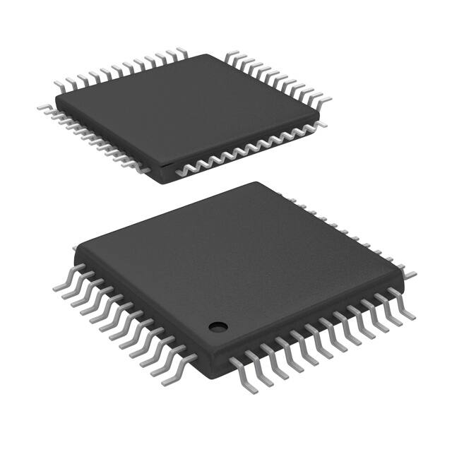
48-Pin TQFP and QFN Packages
APPLICATIONS
D Optical Networking (DWDM, MEMS Based
Switching)
Spectrum Analyzers
High Speed Data Acquisition Systems
D
D
D High Speed Close-Loop Systems
D Telecommunication
D Ultra-Sound Detection
DESCRIPTION
The ADS7881 is a 12-bit 4-MSPS A-to-D converter with
2.5-V internal reference. The device includes a capacitor
based SAR A/D converter with inherent sample and hold.
The device offers a 12-bit parallel interface with an
additional byte mode that provides easy interface with 8-bit
processors. The device has a pseudo-differential input
stage.
The −IN swing of ±200 mV is useful to compensate for
ground voltage mismatch between the ADC and sensor
and also to cancel common-mode noise. With nap mode
enabled, the device operates at lower power when used at
lower conversion rates. The device is available in 48-pin
TQFP and QFN packages.
BYTE
SAR
+IN
−IN
+
_
Output
Latches
and
3-State
Drivers
CDAC
Comparator
12/8-Bit Parallel
Data Output Bus
REFIN
CLOCK
REFOUT
2.5 V
Internal
Reference
Conversion
and
Control Logic
PWD/RST
CONVST
BUSY
CS
RD
A_PWD
Please be aware that an important notice concerning availability, standard warranty, and use in critical applications of Texas Instruments
semiconductor products and disclaimers thereto appears at the end of this data sheet.
�������
�� ���� ������!"��� �# $%��&�" !# �� '%()�$!"��� *!"&+ ���*%$"#
$������ "� #'&$���$!"���# '&� ",& "&��# �� �&-!#
�#"�%�&�"# #"!�*!�* .!��!�"/+
���*%$"��� '��$&##��0 *�&# ��" �&$&##!��)/ ��$)%*& "&#"��0 �� !)) '!�!�&"&�#+
Copyright 2003 − 2005, Texas Instruments Incorporated
��������
www.ti.com
SLAS400B − SEPTEMBER 2003 − REVISED NOVEMBER 2005
This integrated circuit can be damaged by ESD. Texas Instruments recommends that all integrated circuits be handled with appropriate
precautions. Failure to observe proper handling and installation procedures can cause damage.
ESD damage can range from subtle performance degradation to complete device failure. Precision integrated circuits may be more susceptible to
damage because very small parametric changes could cause the device not to meet its published specifications.
ORDERING INFORMATION
MODEL
MAXIMUM
INTEGRAL
LINEARITY
(LSB)
MAXIMUM
DIFFERENTIAL
LINEARITY
(LSB)
±1
NO MISSING
CODES AT
RESOLUTION
(BIT)
PACKAGE
TYPE
12
48-Pin
TQFP
±1
PACKAGE
DESIGNATOR
PFB
TEMPERATURE
RANGE
ORDERING
INFORMATION
TRANSPORT
MEDIA QUANTITY
ADS7881IPFBT
Tape and reel
250
ADS7881IPFBR
Tape and reel
1000
ADS7881IRGZT
Tape and reel
250
ADS7881IRGZR
Tape and reel
2500
−40°C to 85°C
ADS7881
±1
±1
12
48-Pin
QFN
RGZ
−40°C to 85°C
NOTE: For most current package and ordering information, see the Package Option Addendum at the end of this document, or see the TI web site
at www.ti.com.
ABSOLUTE MAXIMUM RATINGS
over operating free-air temperature range(1)
UNIT
+IN to AGND
−0.3 V to +VA + 0.1 V
−IN to AGND
−0.3 V to 0.5 V
+VA to AGND
−0.3 V to 7 V
+VBD to BDGND
−0.3 V to 7 V
Digital input voltage to GND
−0.3 V to (+VBD + 0.3 V)
Digital output to GND
−0.3 V to (+VBD + 0.3 V)
Operating temperature range
−40°C to 85°C
Storage temperature range
−65°C to 150°C
Junction temperature (TJmax)
150°C
Power dissipation
TQFP and QFN packages
Lead temperature, soldering
θJA Thermal impedance
Vapor phase (60 sec)
Infrared (15 sec)
(TJ Max–TA)/ θJA
86°C/W
215°C
220°C
(1) Stresses beyond those listed under “absolute maximum ratings” may cause permanent damage to the device. These are stress ratings only, and
functional operation of the device at these or any other conditions beyond those indicated under “recommended operating conditions” is not
implied. Exposure to absolute-maximum-rated conditions for extended periods may affect device reliability.
2
��������
www.ti.com
SLAS400B − SEPTEMBER 2003 − REVISED NOVEMBER 2005
SPECIFICATIONS
TA = −40°C to 85°C, +VA = 5 V, +VBD = 5 V or 3.3 V, Vref = 2.5 V, fsample = 4 MHz (unless otherwise noted)
PARAMETER
TEST CONDITIONS
MIN
TYP
MAX
UNIT
ANALOG INPUT
Full-scale input span(1)
Absolute input range
+IN – (−IN)
0
+IN
−0.2
−IN
−0.2
Input capacitance
Input leakage current
Vref
Vref + 0.2
+0.2
V
V
27
pF
500
pA
12
Bits
SYSTEM PERFORMANCE
Resolution
No missing codes
Integral linearity(2)
12
−1
±0.6
1
Bits
LSB(3)
LSB(3)
Differential linearity
Offset error(4)
−1
±0.6
1
External reference
−1.5
±0.25
1.5
mV
Gain error(4)
External reference
−2
±0.75
2
mV
Common-mode rejection ratio
With common mode input signal = 200
mVp−p at 1 MHz
60
dB
Power supply rejection
At FF0H output code,
+VA = 4.75 V to 5.25 V , Vref = 2.50 V
80
dB
SAMPLING DYNAMICS
Conversion time
Acquisition time
+VDB = 5 V
185
+VDB = 3 V
+VDB = 5 V
50
+VDB = 3 V
45
200
nsec
205
nsec
65
nsec
nsec
Maximum throughput rate
4
MHz
Aperture delay
2
nsec
Aperture jitter
20
psec
Step response
50
nsec
Over voltage recovery
50
nsec
DYNAMIC CHARACTERISTICS
Total harmonic distortion(5)
VIN = 2.496 Vp−p at 100 kHz/2.5 Vref
VIN = 2.496 Vp−p at 1 MHz/2.5 Vref
−91
−88.5
VIN = 2.496 Vp−p at 1.8 MHz/2.5 Vref
VIN = 2.496 Vp−p at 100 kHz/2.5 Vref
SNR
VIN = 2.496 Vp−p at 1 MHz/2.5 Vref
VIN = 2.496 Vp−p at 1.8 MHz/2.5 Vref
SINAD
VIN = 2.496 Vp−p at 100 kHz/2.5 Vref
VIN = 2.496 Vp−p at 1 MHz/2.5 Vref
SFDR
VIN = 2.496 Vp−p at 1.8 MHz/2.5 Vref
VIN = 2.496 Vp−p at 1 MHz/2.5 Vref
−86
dB
74
71.5
69
71
dB
69.7
71.5
69
71
dB
68.3
−3 dB Small signal bandwidth
90
dB
50
MHz
EXTERNAL REFERENCE INPUT
Input VREF range
Resistance(6)
2.4
To internal reference voltage
2.5
500
2.6
V
kΩ
3
��������
www.ti.com
SLAS400B − SEPTEMBER 2003 − REVISED NOVEMBER 2005
SPECIFICATIONS Continued
TA = −40°C to 85°C, +VA = 5 V, +VBD = 5 V or 3.3 V, Vref = 2.5 V, fsample = 4 MHz (unless otherwise noted)
PARAMETER
TEST CONDITIONS
MIN
TYP
MAX
UNIT
INTERNAL REFERENCE OUTPUT
From 95% (+VA), with 1-µF storage
capacitor on REFOUT to AGND
Start-up time
VREF Range
Source current
IOUT=0
Line regulation
+VA = 4.75 V to 5.25 V
Drift
IOUT = 0
2.47
2.5
Static load
120
msec
2.53
V
10
µA
1
mV
25
PPM/C
DIGITAL INPUT/OUTPUT
Logic family
Logic level
CMOS
VIH
VIL
IIH = 5 µA
IIL = 5 µA
VOH
VOL
IOH = 2 TTL loads
IOL = 2 TTL loads
+VBD −1
−0.3
+VBD + 0.3
0.8
V
+VBD − 0.6
0
+VBD
0.4
V
V
V
Straight
Binary
Data format
POWER SUPPLY REQUIREMENTS
Power supply voltage
+VBD
+VA
2.7
3.3
5.25
V
4.75
5
5.25
V
Supply current, +VA, 4 MHz sample rate
Power dissipation, 4 MHz sample rate
+VA = 5 V
19
22
mA
95
110
mW
2
3
NAP MODE
Supply current, +VA
Power-up time(7)
60
mA
nsec
POWER DOWN
Supply current, +VA
Power down time(8)
Power up time
2
2.5
µA
From simulation results
10
µsec
1-µF Storage capacitor on REFOUT to
AGND
25
msec
4
Numbers
Invalid conversions after power up or reset
TEMPERATURE RANGE
Operating free-air
−40
(1) Ideal input span; does not include gain or offset error.
(2) This is endpoint INL, not best fit.
(3) LSB means least significant bit.
(4) Measured relative to actual measured reference.
(5) Calculated on the first nine harmonics of the input frequency.
(6) Can vary ±20%.
(7) Minimum acquisition time for first sampling after the end of nap state must be 60 nsec more than normal.
(8) Time required to reach level of 2.5 µA.
4
85
°C
��������
www.ti.com
SLAS400B − SEPTEMBER 2003 − REVISED NOVEMBER 2005
TIMING REQUIREMENTS
All specifications typical at −40°C to 85°C, +VA = +5 V, +VBD = +5 V (see Notes 1, 2, 3, and 4)
PARAMETER
Conversion time
Acquisition time
SYMBOL
t(conv)
t(acq)
MIN
50
TYP
MAX
UNITS
REF FIG.
185
200
ns
5
ns
5
ns
3
ns
1
ns
1
ns
1
ns
1
ns
2
ns
2
ns
2
ns
2
65
SAMPLING AND CONVERSION START
Hold time CS low to CONVST high (with BUSY high)
Delay CONVST high to acquisition start
Hold time, CONVST high to CS high with BUSY low
Hold time, CONVST low to CS high
Delay CONVST low to BUSY high
CS width for acquisition or conversion to start
Delay CS low to acquisition start with CONVST high
Pulse width, from CS low to CONVST low for acquisition to start
Delay CS low to BUSY high with CONVST low
Quiet sampling time(3)
th1
td1
10
th2
th3
10
td2
tw3
td3
tw1
2
4
5
10
40
20
2
4
5
20
td4
40
25
ns
CONVERSION ABORT
Setup time CONVST high to CS low with BUSY high
Delay time CS low to BUSY low with CONVST high
ts1
td5
15
ns
4
20
ns
4
td6
td7
25
ns
5
25
ns
5
td9
td11
25
ns
5
20
ns
5
t1
td8
25
ns
5
25
ns
6
td10
t2
25
ns
6
25
ns
6
10
DATA READ
Delay RD low to data valid with CS low
Delay BYTE high to LSB word valid with CS and RD low
Delay time RD high to data 3-state with CS low
Delay time end of conversion to BUSY low
Quiet sampling time RD high to CONVST low
Delay CS low to data valid with RD low
Delay CS high to data 3-state with RD low
Quiet sampling time CS low to CONVST low
BACK-TO-BACK CONVERSION
Delay BUSY low to data valid
td12
tw4
ns
7, 8
Pulse width, CONVST high
60
ns
7, 8
Pulse width, CONVST low
tw5
20
ns
7
tw6
tw7
ns
10
7200
ns
9
ms
9
POWER DOWN/RESET
Pulse width, low for PWD/RST to reset the device
Pulse width, low for PWD/RST to power down the device
45
6140
Delay time, power up after PWD/RST is high
td13
25
(1) All input signals are specified with tr = tf = 5 ns (10% to 90% of +VBD) and timed from a voltage level of (VIL + VIH)/2.
(2) See timing diagram.
(3) Quiet period before conversion start, no data bus activity including data bus 3-state is allowed in this period.
(4) All timings are measured with 20 pF equivalent loads on all data bits and BUSY pin.
5
��������
www.ti.com
SLAS400B − SEPTEMBER 2003 − REVISED NOVEMBER 2005
PIN ASSIGNMENTS
PWD/RST
A_PWD
BYTE
CONVST
CS
RD
+VA
AGND
AGND
+VA
REFM
REFM
PFB PACKAGE
(TOP VIEW)
48 47 46 45 44 43 42 41 40 39 38 37
1
36
BUSY
REFOUT
2
35
BDGND
NC
3
34
+VBD
REFIN
+VA
4
33
NC
AGND
5
32
NC
+IN
6
31
NC
−IN
7
30
NC
AGND
8
29
+VA
9
28
DB0
DB1
+VA
10
27
DB2
AGND
11
26
DB3
AGND 12
25
BDGND
24
+VBD
DB5
DB4
DB6
DB7
DB8
DB9
DB11
DB10
AGND
AGND
+VA
13 14 15 16 17 18 19 20 21 22 23
NC − No connection
BUSY
BDGND
+VBD
NC
NC
NC
NC
DB0
DB1
DB2
DB3
BDGND
RGZ PACKAGE
(TOP VIEW)
+VBD
DB4
DB5
DB6
DB7
DB8
DB9
DB10
DB11
AGND
AGND
+VA
AGND
AGND
AGND
+VA
+VA
−IN
+IN
AGND
NC
+VA
REFOUT
48 47 46 45 44 43 42 41 40 39 38 37
1
36
2
35
3
34
4
33
32
5
31
6
30
7
29
8
28
9
27
10
26
11
25
12
13 14 15 16 17 18 19 20 21 22 23 24
REFIN
A_PWD
PWD/RST
BYTE
CONVST
RD
CS
+VA
AGND
AGND
+VA
REFM
REFM
NC − No internal connection
NOTE: The package thermal pad must be soldered to the printed circuit board for thermal and mechanical performance.
6
��������
www.ti.com
SLAS400B − SEPTEMBER 2003 − REVISED NOVEMBER 2005
TERMINAL FUNCTIONS
NAME
NO. PFB
NO. RGZ
I/O
DESCRIPTION
8-Bit Bus
DATA BUS
BYTE = 0
16-Bit Bus
BYTE = 1
BYTE = 0
DB11
16
28
O
D11 (MSB)
D3
D11 (MSB)
DB10
17
29
O
D10
D2
D10
DB9
18
30
O
D9
D1
D9
DB8
19
31
O
D8
D0 (LSB)
D8
DB7
20
32
O
D7
0
D7
DB6
21
33
O
D6
0
D6
DB5
22
34
O
D5
0
D5
DB4
23
35
O
D4
0
D4
DB3
26
38
O
D3
0
D3
DB2
27
39
O
D2
0
D2
DB1
28
40
O
D1
0
D1
DB0
29
41
O
D0 (LSB)
0
D0 (LSB)
CS
42
6
I
Chip select. Active low signal enables chip operation like acquisition start, conversion start, bus release from 3-state. Refer to the timing diagrams for more details.
CONVST
40
4
I
Conversion start. The rising edge starts the acquisition. The falling edge of this input
ends the acquisition and starts the conversion. Refer to the timing diagrams for more
details.
RD
41
5
I
Active low synchronization pulse for the parallel output. When CS is low, this serves
as the output enable and puts the previous conversion results on the bus.
A_PWD
37
1
I
Nap mode enable, active low
PWD/RST
38
2
I
Active low input, acts as device power down/device reset signal.
BYTE
39
3
I
Byte select input. Used for 8-bit bus reading.
0: No fold back
1: Lower byte D[3:0] is folded back to high byte so D3 is available in D11 place.
36
48
O
Status output. High when a conversion is in progress.
+VBD
24, 34
36, 46
−
Digital power supply for all digital inputs and outputs. Refer to Table 3 for layout
guidelines.
BDGND
25, 35
37, 47
−
Digital ground for all digital inputs and outputs. Short to analog ground plane below
the device.
4, 9, 10, 13,
43, 46
7, 10, 16,
21, 22, 25
−
Analog power supplies. Refer to Table 3 for layout guidelines.
5, 8, 11, 12,
14, 15, 44, 45
8, 9, 17,
20, 23, 24,
26, 27
−
Analog ground pins. Short to analog ground plane below the device.
CONTROL PINS
STATUS OUTPUT
BUSY
POWER SUPPLY
+VA
AGND
ANALOG INPUT
+IN
6
18
I
Noninverting analog input channel
−IN
7
19
I
Inverting analog input channel
REFIN
1
13
I
Reference (positive) input. Needs to be decoupled with REFM pin using 0.1-µF bypass capacitor and 1-µF storage capacitor.
REFOUT
2
14
O
Internal reference output. To be shorted to REFIN pin when internal reference is used.
Do not connect to REFIN pin when external reference is used. Always needs to be
decoupled with AGND using 0.1-µF bypass capacitor.
47, 48
11, 12
I
Reference ground. Connect to analog ground plane.
3, 30, 31, 32,
33
15, 42, 43,
44, 45
−
No connection
REFM
NC
7
��������
www.ti.com
SLAS400B − SEPTEMBER 2003 − REVISED NOVEMBER 2005
DESCRIPTION AND TIMING DIAGRAMS
SAMPLING AND CONVERSION START
There are three ways to start sampling. The rising edge of CONVST starts sampling with CS and BUSY being low
(see Figure 1) or it can be started with the falling edge of CS when CONVST is high and BUSY is low (see
Figure 2). Sampling can also be started with an internal conversion end (before BUSY falling edge) with CS
being low and CONVST high before an internal conversion end (see Figure 3). Also refer to the section DEVICE
OPERATION AND DATA READ IN BACK-TO-BACK CONVERSION for more details.
A conversion can be started two ways (a conversion start is the end of sampling). Either with the falling edge
of CONVST when CS is low (see Figure 1) or the falling edge of CS when CONVST is low (see Figure 2). A
clean and low jitter falling edge of these respective signals triggers a conversion start and is important to the
performance of the converter. The BUSY pin is brought high immediately following the CONVST falling edge.
BUSY stays high throughout the conversion process and returns low when the conversion has ended.
th2
th3
CS
CONVST
td1
td2
BUSY
t(acq)
Figure 1. Sampling and Conversion Start Control With CONVST Pin
tw3
tw3
CS
td4
CONVST
td3
tw1
BUSY
t(acq)
Figure 2. Sampling and Conversion Start Control With CS Pin
CS
th1
tw5
CONVST
tw4
BUSY
td2
t(acq)
Figure 3. Sampling Start With CS Low and CONVST High (Back-to-Back)
8
��������
www.ti.com
SLAS400B − SEPTEMBER 2003 − REVISED NOVEMBER 2005
CONVERSION ABORT
The falling edge of CS aborts the conversion while BUSY is high and CONVST is high (see Figure 4). The device
outputs FE0 (hex) to indicate a conversion abort.
td5
BUSY
tsu1
CONVST
CS
RD
1111 1110 0000
D11−D0
Figure 4. Conversion Abort
DATA READ
Two conditions need to be satisfied for a read operation. Data appears on the D11 through D0 pins (with D11
MSB) when both CS and RD are low. Figure 5 and Figure 6 illustrate the device read operation. The bus is
three-stated if any one of the signals is high.
t1
td2
tw5
CONVST
t(conv)
td1 + t(acq)
BUSY
td11
CS
RD
BYTE
td6
D11−D0
td7
D11−4 & D3−0
td9
D3−0
Figure 5. Read Control Via CS and RD
There are two output formats available. Twelve bit data appears on the bus during a read operation while BYTE
is low. When BYTE is high, the lower byte (D3 through D0 followed by all zeroes) appears on the data bus with
D3 in the MSB. This feature is useful for interfacing with eight bit microprocessors and microcontrollers.
9
��������
www.ti.com
SLAS400B − SEPTEMBER 2003 − REVISED NOVEMBER 2005
t2
CONVST
td1 + t(acq)
BUSY
Conversion No N
td2
CS
BYTE
td7
D11−4 & D3−0
D11−D0
Data For Conv. N−1
td10
D3−0
Data For Conv. N
td8
Figure 6. Read Control Via CS and RD Tied to BDGND
DEVICE OPERATION AND DATA READ IN BACK-TO-BACK CONVERSION
The following two figures illustrate device operation in back-to-back conversion mode. It is possible to operate
the device at any throughput in this mode, but this is the only mode in which the device can be operated at
throughputs exceeding 3.5 MSPS.
A conversion starts on the CONVST falling edge. The BUSY output goes high after a delay (td2). Note that care
must be taken not to abort the conversion (see Figure 4) apart from timing restrictions shown in Figure 7 and
Figure 8. The conversion ends within the conversion time, t(conv), after the CONVST falling edge. The new
acquisition can be immediately started without waiting for the BUSY signal to go low. This can be ensured with
a CONVST high pulse width that is more than or equal to (t0 – t(conv) + 10 nsec) which is tw4 for a 4-MHz operation.
Sample N
CONVST
tw4
t(acq)
tw5
Conversion N
BUSY
td12
D11−D0
t(conv) + td11
Data For Conversion N−1
(Data read Without Latency)
t0 = 250 ns for 4 MSPS Operation
Figure 7. Back-To-Back Operation With CS and RD Low
10
��������
www.ti.com
SLAS400B − SEPTEMBER 2003 − REVISED NOVEMBER 2005
CS
Sample N
th1
CONVST
tw4
t(acq)
tw3
t(conv) + td11
Conversion N
BUSY
Data For Conversion N−1
td12
D11−D0
(Data read Without Latency)
t0 = 250 ns for 4 MSPS Operation
Figure 8. Back-To-Back operation With CS Toggling and RD Low
NAP MODE
The device can be put in nap mode following the sequences shown in Figure 9. This provides substantial power
saving while operating at lower sampling rates.
While operating the device at throughput rates lower than 3.2 MSPS, A_PWD can be held low (see Figure 9).
In this condition, the device goes into the nap state immediately after BUSY goes low and remains in that state
until the next sampling starts. The minimum acquisition time is 60 nsec more than t(acq) as defined in the timing
requirements section.
Alternately, A_PWD can be toggled any time during operation (see Figure 10). This is useful when the system
acquires data at the maximum conversion speed for some period of time (back-to-back conversion) and it does
not acquire data for some time while the acquired data is being processed. During this period, the device can
be put in the nap state to save power. The device remains in the nap state as long as A_PWD is low with BUSY
being low and sampling has not started. The minimum acquisition time for the first sampling after the nap state
is 60 nsec more than t(acq) as defined in the timing requirements section.
A_PWD
(Held Low)
BUSY
SAMPLE
(Internal)
t(acq) + 60 ns
NAP
(Internal Active High)
NOTE: The SAMPLE (Internal) signal is generated as described in the Sampling and Conversion
Start section.
Figure 9. Device Operation While A_PWD is Held Low
11
��������
www.ti.com
SLAS400B − SEPTEMBER 2003 − REVISED NOVEMBER 2005
A_PWD
BUSY
SAMPLE
(Internal)
t(acq) + 60 ns
NAP
(Internal Active High)
NOTE: The SAMPLE (Internal) signal is generated as described in the Sampling and Conversion
Start section.
Figure 10. Device Operation While A_PWD is Toggling
POWERDOWN/RESET
A low level on the PWD/RST pin puts the device in the powerdown phase. This is an asynchronous signal. As
shown in Figure 11, the device is in the reset phase for the first tw6 period after a high-to-low transition of
PWD/RST. During this period the output code is FE0 (hex) to indicate that the device is in the reset phase. The
device powers down if the PWD/RST pin continues to be low for a period of more than tw7. Data is not valid for
the first four conversions after a power-up (see Figure 11) or an end of reset (see Figure 12). The device is
initialized during the first four conversions.
tw7
Valid Conversions
PWD/RST
First 4 Invalid Conversions
BUSY
1
2
3
4
5
td13
D11−D0
1111 1110 0000
Power Down
Phase
RESET Phase
Invalid Data
Valid Data
Figure 11. Device Power Down
tw6
45 ns
PWD/RST
Valid Conversions
First 4 Invalid Conversions
BUSY
D11−D0
1
3
4
5
1111 1110 0000
RESET Phase
Figure 12. Device Reset
12
2
Invalid Data
Valid Data
��������
www.ti.com
SLAS400B − SEPTEMBER 2003 − REVISED NOVEMBER 2005
TYPICAL CHARACTERISTICS(1)
EFFECTIVE NUMBER OF BITS
vs
FREE-AIR TEMPERATURE
HISTOGRAM
(DC CODE SPREAD AT THE CENTER OF CODE)
140000
Count
100000
80000
60000
40000
20000
Count
=0
Count
=1
2046
2047
0
2048
Count
= 192
Count
=0
2049
2050
ENOB − Effective Number of Bits − Bits
120000
12
Count = 130879
+VA = 5 V,
+VBD = 5 V,
Code = 2048,
TA = 255C
11.9
11.8
11.7
11.6
11.5
11.4
11.3
11.2
11.1
11
−40
Code
Figure 13
−20
0
20
40
60
TA − Free-Air Temperature − °C
80
Figure 14
SIGNAL-TO-NOISE AND DISTORTION
vs
FREE-AIR TEMPERATURE
SIGNAL-TO-NOISE RATIO
vs
FREE-AIR TEMPERATURE
72
72
fi = 100 kHz,
+VA = 5 V,
+VBD = 5 V
fi = 100 kHz,
+VA = 5 V,
+VBD = 5 V
71.9
SNR − Signal-to-Noise Ratio − dB
SINAD − Signal-to-Noise and Distortion − dB
fi = 100 kHz,
+VA = 5 V,
+VBD = 5 V
71.8
71.6
71.4
71.2
71.8
71.7
71.6
71.5
71.4
71.3
71.2
71.1
71
−40
71
−20
0
20
40
60
TA − Free-Air Temperature − °C
80
Figure 15
−40
−20
0
20
40
60
TA − Free-Air Temperature − °C
80
Figure 16
(1) At sample rate = 4 MSPS, Vref = 2.5 V external, unless otherwise specified.
13
��������
www.ti.com
SLAS400B − SEPTEMBER 2003 − REVISED NOVEMBER 2005
SPURIOUS FREE DYNAMIC RANGE
vs
FREE-AIR TEMPERATURE
TOTAL HARMONIC DISTORTION
vs
FREE-AIR TEMPERATURE
−85
fi = 100 kHz,
+VA = 5 V,
+VBD = 5 V
THD − Total Harmonic Distortion − dB
SFDR − Spurious Free Dynamic Range − dB
105
100
95
90
85
−40
−20
0
20
40
60
TA − Free-Air Temperature − °C
fi = 100 kHz,
+VA = 5 V,
+VBD = 5 V
−90
−95
−100
−40
80
−20
0
20
40
60
TA − Free-Air Temperature − °C
Figure 17
Figure 18
EFFECTIVE NUMBER OF BITS
vs
INPUT FREQUENCY
SIGNAL-TO-NOISE AND DISTORTION
vs
INPUT FREQUENCY
73
+VA = 5 V,
+VBD = 5 V,
TA = 25°C,
SINAD − Signal-to-Nois and Distortion − dB
ENOB − Effective Number of Bits − Bits
12
11.5
11
10.5
10
+VA = 5 V,
+VBD = 5 V,
TA = 25°C,
72
71
70
69
68
67
66
65
0
300
600
900
1200
1500
fi − Input Frequency − kHz
Figure 19
14
80
1800
0
300
600
900
1200
1500
fi − Input Frequency − kHz
Figure 20
1800
��������
www.ti.com
SLAS400B − SEPTEMBER 2003 − REVISED NOVEMBER 2005
SPURIOUS FREE DYNAMIC RANGE
vs
INPUT FREQUENCY
SIGNAL-TO-NOISE RATIO
vs
INPUT FREQUENCY
105
73
SNR − Signal-to-Noise Ratio − dB
72
SFDR − Spurious Free Dynamic Range − dB
+VA = 5 V,
+VBD = 5 V,
TA = 25°C,
71
70
69
68
67
66
65
+VA = 5 V,
+VBD = 5 V,
TA = 25°C,
100
95
90
85
80
75
70
65
60
0
300
600
900
1200
1500
fi − Input Frequency − kHz
0
1800
300
600
900
1200
1500
fi − Input Frequency − kHz
Figure 21
Figure 22
GAIN ERROR
vs
SUPPLY VOLTAGE
TOTAL HARMONIC DISTORTION
vs
INPUT FREQUENCY
−60
0.9
+VBD = 5 V,
TA = 25°C,
+VA = 5 V,
+VBD = 5 V,
TA = 25°C,
−65
−70
E G − Gain Error − mV
THD − Total Harmonic Distortion − dB
1800
−75
−80
−85
−90
0.85
0.8
0.75
−95
−100
0
300
600
900
1200
fi − Input Frequency − kHz
Figure 23
1500
1800
0.7
4.75 4.8 4.85 4.9 4.95 5 5.05 5.1 5.15 5.2 5.25
+VA − Supply Voltage − V
Figure 24
15
��������
www.ti.com
SLAS400B − SEPTEMBER 2003 − REVISED NOVEMBER 2005
GAIN ERROR
vs
FREE-AIR TEMPERATURE
OFFSET ERROR
vs
SUPPLY VOLTAGE
1.5
0.5
+VA = 5 V,
+VBD = 5 V,
+VBD = 5 V,
TA = 25°C,
1.25
E G − Gain Error − mV
EO − Offset Error − mV
0.4
0.3
0.2
0.1
1
0.75
0.5
0.25
0
4.75 4.8 4.85 4.9 4.95 5 5.05 5.1 5.15 5.2 5.25
+VA − Supply Voltage − V
0
−40
−20
0
20
40
60
TA − Free-Air Temperature − °C
Figure 25
Figure 26
POWER DISSIPATION
vs
SAMPLE RATE
OFFSET ERROR
vs
FREE-AIR TEMPERATURE
100
1
+VA = 5 V,
+VBD = 5 V
0.5
EO − Offset Error − mV
+VA = 5 V,
+VBD = 5 V,
TA = 25°C,
90
PD− Power Dissipation − mW
0.75
80
0.25
0
−0.25
80
NAP Disabled
70
60
NAP Enabled
50
40
30
−0.5
20
−0.75
−1
−40
10
0
−20
0
20
40
60
TA − Free-Air Temperature − °C
Figure 27
16
80
0
500 1000 1500 2000 2500 3000 3500 4000
Sample Rate − KSPS
Figure 28
��������
www.ti.com
SLAS400B − SEPTEMBER 2003 − REVISED NOVEMBER 2005
POWER DISSIPATION
vs
FREE-AIR TEMPERATURE
DIFFERENTIAL NONLINEARITY
vs
FREE-AIR TEMPERATURE
97
1
DNL − Differential Nonlinearity − Bits
PD − Power Dissipation − mW
+VA = 5 V,
+VBD = 5 V
96
95
94
93
−20
0
20
40
60
TA − Free-Air Temperature − °C
80
0.25
0
−0.25
Min
−0.5
−0.75
−20
0
60
80
INTERNAL REFERENCE OUTPUT
vs
FREE-AIR TEMPERATURE
1
2.505
+VA = 5 V,
+VBD = 5 V
2.5045
Vref − Internal Reference Output − V
INL − Integral Nonlinearity − Bits
40
Figure 30
INTEGRAL NONLINEARITY
vs
FREE-AIR TEMPERATURE
Max
0.5
0.25
0
−0.25
Min
−0.5
−0.75
−1
−40
20
TA − Free-Air Temperature − °C
Figure 29
0.75
Max
0.5
−1
−40
92
−40
+VA = 5 V,
+VBD = 5 V
0.75
+VA = 5 V,
+VBD = 5 V
2.504
2.5035
2.503
2.5025
2.502
2.5015
2.501
2.5005
−20
0
20
40
60
TA − Free-Air Temperature − °C
Figure 31
80
2.5
−40
−20
0
20
40
60
TA − Free-Air Temperature − °C
80
Figure 32
17
��������
www.ti.com
SLAS400B − SEPTEMBER 2003 − REVISED NOVEMBER 2005
INTERNAL REFERENCE OUTPUT
vs
SUPPLY VOLTAGE
2.505
Vref − Internal Reference Output − V
2.5045
+VBD = 5 V,
TA = 255C
2.504
2.5035
2.503
2.5025
2.502
2.5015
2.501
2.5005
2.5
4.75 4.8 4.85 4.9 4.95 5 5.05 5.1 5.15 5.2 5.25
+VA − Supply Voltage − V
Figure 33
DNL − LSB
DIFFERENTIAL NONLINEARITY
1
0.8
0.6
0.4
0.2
+VA = 5 V,
+VBD = 5 V,
TA = 25°C,
Sample Rate = 4 MSPS
0
−0.2
−0.4
−0.6
−0.8
−1
0
1028
2056
3084
4096
3084
4096
Code
Figure 34
INL − LSB
INTEGRAL NONLINEARITY
1
0.8
0.6
0.4
0.2
+VA = 5 V,
+VBD = 5 V,
TA = 25°C,
Sample Rate = 4 MSPS
0
−0.2
−0.4
−0.6
−0.8
−1
FIGURE 36
0
1028
2056
Code
Figure 35
18
��������
www.ti.com
SLAS400B − SEPTEMBER 2003 − REVISED NOVEMBER 2005
FFT
Signal Amplitude − dB
20
+VA = 5 V,
+VBD = 5 V,
TA = 25°C,
Sample Rate = 4 MSPS
0
−20
−40
−60
−80
−100
−120
FIGURE 37
−140
−160
0
0.4
0.8
1.2
f − Frequency − MHz
1.6
2
Figure 36
19
��������
www.ti.com
SLAS400B − SEPTEMBER 2003 − REVISED NOVEMBER 2005
PRINCIPLES OF OPERATION
The ADS7881 is a member of a family of high-speed successive approximation register (SAR) analog-to-digital
converters (ADC). The architecture is based on charge redistribution, which inherently includes a sample/hold
function.
The conversion clock is generated internally. The conversion time is 200 ns max (at 5 V +VBD).
The analog input is provided to two input pins: +IN and −IN. (Note that this is pseudo differential input and there
are restrictions on –IN voltage range.) When a conversion is initiated, the difference voltage between these pins
is sampled on the internal capacitor array. While a conversion is in progress, both inputs are disconnected from
any internal function.
REFERENCE
The ADS7881 has a built-in 2.5-V (nominal value) reference but can operate with an external reference. When
an internal reference is used, pin 2 (REFOUT) should be connected to pin 1 (REFIN) with an 0.1-µF decoupling
capacitor and a 1-µF storage capacitor between pin 2 (REFOUT) and pins 47, 48 (REFM). The internal
reference of the converter is buffered . There is also a buffer from REFIN to CDAC. This buffer provides isolation
between the external reference and the CDAC and also recharges the CDAC during conversion. It is essential
to decouple REFOUT to AGND with a 0.1-µF capacitor while the device operates with an external reference.
ANALOG INPUT
When the converter enters hold mode, the voltage difference between the +IN and −IN inputs is captured on
the internal capacitor array. The voltage on the −IN input is limited to between –0.2 V and 0.2 V, thus allowing
the input to reject a small signal which is common to both the +IN and −IN inputs. The +IN input has a range
of –0.2 V to (+Vref +0.2 V). The input span (+IN – (−IN)) is limited from 0 V to VREF.
The input current on the analog inputs depends upon a number of factors: sample rate, input voltage, signal
frequency, and source impedance. Essentially, the current into the ADS7881 charges the internal capacitor
array during the sample period. After this capacitance has been fully charged, there is no further input current
(this may not happen when a signal is moving continuously). The source of the analog input voltage must be
able to charge the input capacitance (27 pF) to better than a 12-bit settling level with a step input within the
acquisition time of the device. The step size can be selected equal to the maximum voltage difference between
two consecutive samples at the maximum signal frequency. (Refer to Figure 39 for the suggested input circuit.)
When the converter goes into hold mode, the input impedance is greater than 1 GΩ.
Care must be taken regarding the absolute analog input voltage. To maintain the linearity of the converter, both
−IN and +IN inputs should be within the limits specified. Outside of these ranges, the converter’s linearity may
not meet specifications.
Care should be taken to ensure that +IN and −IN see the same impedance to the respective sources. (For
example, both +IN and −IN are connected to a decoupling capacitor through a 21-Ω resistor as shown in
Figure 39.) If this is not observed, the two inputs could have different settling times. This may result in an offset
error, gain error, or linearity error which changes with temperature and input voltage.
DIGITAL INTERFACE
TIMING AND CONTROL
Refer to the SAMPLING AND CONVERSION START section and the CONVERSION ABORT section.
READING DATA
The ADS7881 outputs full parallel data in straight binary format as shown in Table 1. The parallel output is active
when CS and RD are both low. There is a minimal quiet sampling period requirement around the falling edge
of CONVST as stated in the timing requirements section. Data reads or bus three-state operations should not
be attempted within this period. Any other combination of CS and RD three-states the parallel output. Refer to
Table 1 for ideal output codes.
20
��������
www.ti.com
SLAS400B − SEPTEMBER 2003 − REVISED NOVEMBER 2005
Table 1. Ideal Input Voltages and Output Codes(1)
DESCRIPTION
Full scale
ANALOG VALUE
Vref − 1 LSB
Vref/2
Midscale
BINARY CODE
HEX CODE
1111 1111 1111
FFF
1000 0000 0000
800
Midscale − 1 LSB
Vref/2 − 1 LSB
0111 1111 1111
7FF
Zero
0V
0000 0000 0000
000
(1) Full-scale range = Vref and least significant bit (LSB) = Vref/4096
The output data appears as a full 12-bit word (D11−D0) on pins DB11 – DB0 (MSB−LSB) if BYTE is low.
READING THE DATA IN BYTE MODE
The result can also be read on an 8-bit bus for convenience by using pins DB11−DB4. In this case two reads
are necessary; the first as before, leaving BYTE low and reading the 8 most significant bits on pins DB11−DB4,
and then bringing BYTE high. When BYTE is high, the lower bits (D3−D0) followed by all zeros are on pins DB11
− DB4 (refer to Table 2).
These multi-word read operations can be performed with multiple active RD signals (toggling) or with RD tied
low for simplicity.
Table 2. Conversion Data Read Out
DATA READ OUT
BYTE
DB11 − DB4
DB3 − DB0
High
D3 − D0, 0000
All zeroes
Low
D11 − D4
D3 − D0
Also refer to the DATA READ and DEVICE OPERATION AND DATA READ IN BACK-TO-BACK
CONVERSION sections for more details.
Reset
Refer to the POWERDOWN/RESET section for the device reset sequence.
It is recommended to reset the device after power on. A reset can be issued once the power has reached 95%
of its final value.
PWD/RST is an asynchronous active low input signal. A current conversion is aborted no later than 45 ns after
the converter is in the reset mode. In addition, the device outputs a FE0 code to indicate a reset condition. The
converter returns back to normal operation mode immediately after the PWD/RST input is brought high.
Data is not valid for the first four conversions after a device reset.
Powerdown
Refer to the POWERDOWN/RESET section for the device powerdown sequence.
The device enters powerdown mode if a PWD/RST low duration is extended for more than a period of tw7.
The converter goes back to normal operation mode no later than a period of td13 after the PWD/RST input is
brought high.
After this period, normal conversion and sampling operation can be started as discussed in previous sections.
Data is not valid for the first four conversions after a device reset.
Nap Mode
Refer to the NAP MODE section in the DESCRIPTION AND TIMING DIAGRAMS section for information.
21
��������
www.ti.com
SLAS400B − SEPTEMBER 2003 − REVISED NOVEMBER 2005
APPLICATION INFORMATION
LAYOUT
For optimum performance, care should be taken with the physical layout of the ADS7881 circuitry.
As the ADS7881 offers single-supply operation, it is often used in close proximity with digital logic,
micro-controllers, microprocessors, and digital signal processors. The more digital logic present in the design
and the higher the switching speed, the more difficult it is to achieve acceptable performance from the converter.
The basic SAR architecture is sensitive to glitches or sudden changes on the power supply, reference, ground
connections, and digital inputs that occur just prior to the end of sampling (within quiet sampling time) and just
prior to latching the output of the analog comparator during the conversion phase. Thus, driving any single
conversion for an n-bit SAR converter, there are n+1 windows in which large external transient voltages can
affect the conversion result. Such glitches might originate from switching power supplies, nearby digital logic,
or high power devices.
The degree of error in the digital output depends on the reference voltage, layout, and the exact timing of the
external event.
On average, the ADS7881 draws very little current from an external reference as the reference voltage is
internally buffered. If the reference voltage is external and originates from an op amp, make sure that it can drive
the bypass capacitor or capacitors without oscillation. A 0.1-µF bypass capacitor and 1-µF storage capacitor
are recommended from REFIN (pin 1) directly to REFM (pin 48).
The AGND and BDGND pins should be connected to a clean ground point. In all cases, this should be the analog
ground. Avoid connections which are too close to the grounding point of a micro-controller or digital signal
processor. If required, run a ground trace directly from the converter to the power supply entry point. The ideal
layout consists of an analog ground plane dedicated to the converter and associated analog circuitry.
As with the AGND connections, +VA should be connected to a 5-V power supply plane that is separate from
the connection for +VBD and digital logic until they are connected at the power entry point onto the PCB. Power
to the ADS7881 should be clean and well bypassed. A 0.1-µF ceramic bypass capacitor should be placed as
close to the device as possible. See Table 3 for the placement of capacitor. In addition to a 0.1-µF capacitor,
a 1-µF capacitor is recommended. In some situations, additional bypassing may be required, such as a 100-µF
electrolytic capacitor or even a Pi filter made up of inductors and capacitors, all designed to essentially low-pass
filter the 5-V supply, removing the high frequency noise.
Table 3. Power Supply Decoupling Capacitor Placement
POWER SUPPLY PLANE
CONVERTER ANALOG SIDE
SUPPLY PINS
Pairs of pins that require a shortest path to decoupling
capacitors
(4,5), (9,8), (10,11), (13, 15), (43, 44) (46, 45)
Pins that require no decoupling
14, 12
Analog 5 V
+VA
0.1 µF
1 µF
ADS7881
AGND
AGND
0.1 µF
REFOUT
External
Reference in
REFIN
1 µF
0.1 µF
REFM
AGND
21 Ω
Analog Input
Circuit
21 Ω
+IN
−IN
Figure 37. Using External Reference
22
CONVERTER DIGITAL SIDE
(24, 25), (34, 35)
��������
www.ti.com
SLAS400B − SEPTEMBER 2003 − REVISED NOVEMBER 2005
Analog 5 V
+VA
0.1 µF
1 µF
ADS7881
AGND
AGND
REFOUT
0.1 µF
1 µF
REFIN
REFM
AGND
21 Ω
Analog Input
Circuit
21 Ω
+IN
−IN
Figure 38. Using Internal Reference
130 pF
604 Ω
Signal Input
2.5 V DC
3 kΩ
604 Ω
_
100 Ω
THS4211
+
1 kΩ
12 Ω
21 Ω
21 Ω
150 pF
1 nF
+IN
ADS7881
−IN
AGND
AGND
Figure 39. Typical Analog Input Circuit
GPIO
CS
GPIO
BYTE
GPIO
CONVST
Microcontroller
ADS7881
P[7:0]
DB[11:4]
RD
RD
INT
BUSY
Figure 40. Interfacing With Microcontroller
23
�PACKAGE MATERIALS INFORMATION
www.ti.com
1-Sep-2021
TAPE AND REEL INFORMATION
*All dimensions are nominal
Device
ADS7881IRGZR
Package Package Pins
Type Drawing
VQFN
RGZ
48
SPQ
Reel
Reel
A0
Diameter Width (mm)
(mm) W1 (mm)
2500
330.0
16.4
Pack Materials-Page 1
7.3
B0
(mm)
K0
(mm)
P1
(mm)
W
Pin1
(mm) Quadrant
7.3
1.5
12.0
16.0
Q2
�PACKAGE MATERIALS INFORMATION
www.ti.com
1-Sep-2021
*All dimensions are nominal
Device
Package Type
Package Drawing
Pins
SPQ
Length (mm)
Width (mm)
Height (mm)
ADS7881IRGZR
VQFN
RGZ
48
2500
350.0
350.0
43.0
Pack Materials-Page 2
�GENERIC PACKAGE VIEW
RGZ 48
VQFN - 1 mm max height
PLASTIC QUADFLAT PACK- NO LEAD
7 x 7, 0.5 mm pitch
Images above are just a representation of the package family, actual package may vary.
Refer to the product data sheet for package details.
4224671/A
www.ti.com
�PACKAGE OUTLINE
RGZ0048A
VQFN - 1 mm max height
PLASTIC QUADFLAT PACK- NO LEAD
A
7.1
6.9
B
(0.1) TYP
7.1
6.9
PIN 1 INDEX AREA
SIDE WALL DETAIL
OPTIONAL METAL THICKNESS
(0.45) TYP
CHAMFERED LEAD
CORNER LEAD OPTION
1 MAX
C
SEATING PLANE
0.05
0.00
0.08 C
2X 5.5
5.15±0.1
(0.2) TYP
24
13
44X 0.5
12
25
SYMM
2X
5.5
1
PIN1 ID
(OPTIONAL)
SEE LEAD OPTION
SEE SIDE WALL
DETAIL
36
48
SYMM
37
48X 0.5
0.3
48X 0.30
0.18
0.1
0.05
C A B
C
4219044/D 02/2022
NOTES:
1.
2.
3.
All linear dimensions are in millimeters. Any dimensions in parenthesis are for reference only. Dimensioning and tolerancing
per ASME Y14.5M.
This drawing is subject to change without notice.
The package thermal pad must be soldered to the printed circuit board for optimal thermal and mechanical performance.
www.ti.com
�EXAMPLE BOARD LAYOUT
RGZ0048A
VQFN - 1 mm max height
PLASTIC QUADFLAT PACK- NO LEAD
2X (6.8)
( 5.15)
SYMM
48X (0.6)
37
48
48X (0.24)
1
44X (0.5)
2X
(5.5)
36
SYMM
2X
(6.8)
2X
(1.26)
2X
(1.065)
(R0.05)
TYP
25
12
21X (Ø0.2) VIA
TYP
13
24
2X (1.26)
2X (1.065)
2X (5.5)
LAND PATTERN EXAMPLE
SCALE: 15X
0.07 MIN
ALL AROUND
0.07 MAX
ALL AROUND
EXPOSED METAL
SOLDER MASK
OPENING
EXPOSED METAL
METAL
NON SOLDER MASK
DEFINED
(PREFERRED)
SOLDER MASK
OPENING
SOLDER MASK
DEFINED
SOLDER MASK DETAILS
METAL UNDER
SOLDER MASK
4219044/D 02/2022
NOTES: (continued)
4.
5.
This package is designed to be soldered to a thermal pad on the board. For more information, see Texas Instruments literature
number SLUA271 (www.ti.com/lit/slua271).
Vias are optional depending on application, refer to device data sheet. If any vias are implemented, refer to their locations shown
on this view. It is recommended that vias under paste be filled, plugged or tented.
www.ti.com
�EXAMPLE STENCIL DESIGN
RGZ0048A
VQFN - 1 mm max height
PLASTIC QUADFLAT PACK- NO LEAD
2X (6.8)
SYMM
48X (0.6)
( 1.06)
37
48
48X (0.24)
1
44X (0.5)
2X
(5.5)
36
SYMM
2X
2X (6.8)
(0.63)
2X
(1.26)
(R0.05)
TYP
25
12
13
2X (0.63)
2X
(1.26)
24
2X (5.5)
SOLDER PASTE EXAMPLE
BASED ON 0.125 mm THICK STENCIL
EXPOSED PAD
67% PRINTED COVERAGE BY AREA
SCALE: 15X
4219044/D 02/2022
NOTES: (continued)
6.
Laser cutting apertures with trapezoidal walls and rounded corners may offer better paste release. IPC-7525 may have alternate
design recommendations.
www.ti.com
�MECHANICAL DATA
MTQF019A – JANUARY 1995 – REVISED JANUARY 1998
PFB (S-PQFP-G48)
PLASTIC QUAD FLATPACK
0,27
0,17
0,50
36
0,08 M
25
37
24
48
13
0,13 NOM
1
12
5,50 TYP
7,20
SQ
6,80
9,20
SQ
8,80
Gage Plane
0,25
0,05 MIN
0°– 7°
1,05
0,95
Seating Plane
0,75
0,45
0,08
1,20 MAX
4073176 / B 10/96
NOTES: A. All linear dimensions are in millimeters.
B. This drawing is subject to change without notice.
C. Falls within JEDEC MS-026
POST OFFICE BOX 655303
• DALLAS, TEXAS 75265
��IMPORTANT NOTICE AND DISCLAIMER
TI PROVIDES TECHNICAL AND RELIABILITY DATA (INCLUDING DATA SHEETS), DESIGN RESOURCES (INCLUDING REFERENCE
DESIGNS), APPLICATION OR OTHER DESIGN ADVICE, WEB TOOLS, SAFETY INFORMATION, AND OTHER RESOURCES “AS IS”
AND WITH ALL FAULTS, AND DISCLAIMS ALL WARRANTIES, EXPRESS AND IMPLIED, INCLUDING WITHOUT LIMITATION ANY
IMPLIED WARRANTIES OF MERCHANTABILITY, FITNESS FOR A PARTICULAR PURPOSE OR NON-INFRINGEMENT OF THIRD
PARTY INTELLECTUAL PROPERTY RIGHTS.
These resources are intended for skilled developers designing with TI products. You are solely responsible for (1) selecting the appropriate
TI products for your application, (2) designing, validating and testing your application, and (3) ensuring your application meets applicable
standards, and any other safety, security, regulatory or other requirements.
These resources are subject to change without notice. TI grants you permission to use these resources only for development of an
application that uses the TI products described in the resource. Other reproduction and display of these resources is prohibited. No license
is granted to any other TI intellectual property right or to any third party intellectual property right. TI disclaims responsibility for, and you
will fully indemnify TI and its representatives against, any claims, damages, costs, losses, and liabilities arising out of your use of these
resources.
TI’s products are provided subject to TI’s Terms of Sale or other applicable terms available either on ti.com or provided in conjunction with
such TI products. TI’s provision of these resources does not expand or otherwise alter TI’s applicable warranties or warranty disclaimers for
TI products.
TI objects to and rejects any additional or different terms you may have proposed. IMPORTANT NOTICE
Mailing Address: Texas Instruments, Post Office Box 655303, Dallas, Texas 75265
Copyright © 2022, Texas Instruments Incorporated
�


 工商网监
湘ICP备2023018690号
工商网监
湘ICP备2023018690号
