Burr Brown Products from Texas Instruments
AD S8
®
365
ADS8365
SBAS362A – AUGUST 2006 – REVISED SEPTEMBER 2006
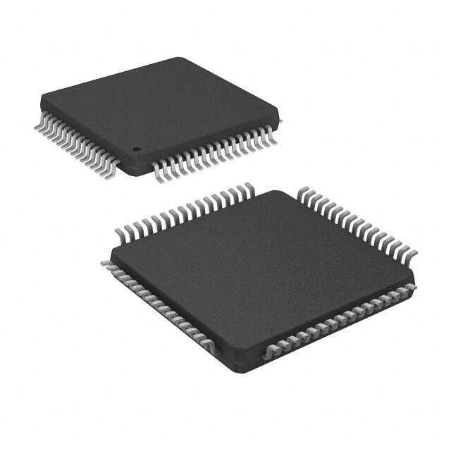
16-Bit, 250kSPS, 6-Channel, Simultaneous Sampling SAR ANALOG-TO-DIGITAL CONVERTERS
FEATURES
• • • • • Six Input Channels Fully Differential Inputs Six Independent 16-Bit ADCs 4µs Total Throughput per Channel Low Power: 200mW in Normal Mode 5mW in Nap Mode 50µW in Power-Down Mode TQFP-64 Package Package
DESCRIPTION
The ADS8365 includes six, 16-bit, 250kSPS analog-to-digital converters (ADCs) with six fully differential input channels grouped into three pairs for high-speed simultaneous signal acquisition. Inputs to the sample-and-hold amplifiers are fully differential and are maintained differential to the input of the ADC. This architecture provides excellent common-mode rejection of 80dB at 50kHz, which is important in high-noise environments. The ADS8365 offers a flexible, high-speed parallel interface with a direct address mode, a cycle, and a FIFO mode. The output data for each channel is available as a 16-bit word.
• • • •
APPLICATIONS
Motor Control Multi-Axis Positioning Systems 3-Phase Power Control
CH A0+
CH A0-
CDAC S/H Amp Comp
SAR HOLDA
CH A1+ CH A1S/H Amp CH B0+ CH B0S/H Amp
CDAC Comp
Interface
Conversion and Control CDAC Comp
A0 A1 A2 ADD NAP RD WR CS FD EOC CLK RESET BYTE 16
SAR HOLDB CH B1+ CH B1S/H Amp CH C0+ CH C0S/H Amp SAR HOLDC CH C1+ CH C1S/H Amp REFIN REFOUT Internal 2.5V Reference CDAC Comp FIFO Register and 6x CDAC Comp
Data Input/Output CDAC Comp
Please be aware that an important notice concerning availability, standard warranty, and use in critical applications of Texas Instruments semiconductor products and disclaimers thereto appears at the end of this data sheet. All trademarks are the property of their respective owners.
PRODUCTION DATA information is current as of publication date. Products conform to specifications per the terms of the Texas Instruments standard warranty. Production processing does not necessarily include testing of all parameters.
Copyright © 2006, Texas Instruments Incorporated
�ADS8365
www.ti.com
SBAS362A – AUGUST 2006 – REVISED SEPTEMBER 2006
This integrated circuit can be damaged by ESD. Texas Instruments recommends that all integrated circuits be handled with appropriate precautions. Failure to observe proper handling and installation procedures can cause damage. ESD damage can range from subtle performance degradation to complete device failure. Precision integrated circuits may be more susceptible to damage because very small parametric changes could cause the device not to meet its published specifications.
ORDERING INFORMATION (1)
MAXIMUM NO INTEGRAL MISSING LINEARITY CODES ERROR ERROR PACKAGEPACKAGE (LSB) (LSB) LEAD DESIGNATOR ±4 14 TQFP-64 PAG
PRODUCT ADS8365
SPECIFIED TEMPERATURE RANGE –40°C to +85°C
PACKAGE MARKING ADS8365I
ORDERING NUMBER ADS8365IPAG ADS8365IPAGR
TRANSPORT MEDIA, QUANTITY Tray, 96 Tape and Reel, 1500
(1)
For the most current package and ordering information, see the Package Option Addendum located at the end of this data sheet, or see the TI website at www.ti.com.
ABSOLUTE MAXIMUM RATINGS (1)
over operating free-air temperature range (unless otherwise noted)
ADS8365 Supply voltage, AGND to AVDD Supply voltage, BGND to BVDD Analog input voltage range Reference input voltage range Digital input voltage range Ground voltage differences, AGND to BGND Voltage differences, BVDD to AGND Input current to any pin except supply Power dissipation Operating virtual junction temperature range, TJ Operating free-air temperature range, TA Storage temperature range, TSTG (1) –0.3 to 6 –0.3 to 6 AGND – 0.3 to AVDD + 0.3 AGND – 0.3 to AVDD + 0.3 BGND – 0.3 to BVDD + 0.3 ±0.3 –0.3 to 6 –20 to 20 See Dissipation Ratings Table –40 to +150 –40 to +85 –65 to +150 °C °C °C UNIT V V V V V V V mA
Stresses beyond those listed under Absolute Maximum Ratings may cause permanent damage to the device. These are stress ratings only, and functional operation of the device at these or any other conditions beyond those indicated under Recommended Operating Conditions is not implied. Exposure to absolute-maximum rated conditions for extended periods may affect device reliability.
DISSIPATION RATINGS
BOARD Low-K (1) High-K (2) (1) (2) PACKAGE PAG PAG RθJC 8.6°C/W 8.6°C/W RθJA 68.5°C/W 42.8°C/W DERATING FACTOR ABOVE TA = +25°C 14.598mW/°C 23.364mW/°C TA ≤ +25°C POWER RATING 1824mW 2920mW TA = +70°C POWER RATING 1168mW 1869mW TA = +85°C POWER RATING 949mW 1519mW
The JEDEC Low K (1s) board design used to derive this data was a 3-inch x 3-inch, two-layer board with 2-ounce copper traces on top of the board. The JEDEC High K (2s2p) board design used to derive this data was a 3-inch x 3-inch, multilayer board with 1-ounce internal power and ground planes, and 2-ounce copper traces on the top and bottom of the board.
2
Submit Documentation Feedback
�ADS8365
www.ti.com
SBAS362A – AUGUST 2006 – REVISED SEPTEMBER 2006
RECOMMENDED OPERATING CONDITIONS
MIN Supply voltage, AVDD to AGND Supply voltage, BVDD to BGND Reference input voltage Operating common-mode signal, –IN Analog inputs, +IN – (–IN) Operating junction temperature range, TJ Low-voltage levels 5V logic levels 4.75 2.7 4.5 1.5 2.2 0 –40 5 2.5 2.5 NOM 5 MAX 5.25 3.6 5.5 2.6 2.8 ±VREF +125 UNIT V V V V V V °C
ELECTRICAL CHARACTERISTICS: 100kSPS
Over recommended operating free-air temperature range at –40°C to +85°C, AVDD = 5V, BVDD = 3V, VREF = internal +2.5V, fCLK = 2MHz, and fSAMPLE = 100kSPS, unless otherwise noted.
ADS8365 PARAMETER ANALOG INPUT Full-scale range Operating common-mode signal Input resistance Input capacitance Input leakage current Differential input resistance Differential input capacitance Common-mode rejection ratio Bandwidth DC ACCURACY Resolution No missing codes Integral linearity error Differential nonlinearity Bipolar offset error Bipolar offset error match Bipolar offset error drift Gain error Gain error match Gain error drift Noise Power-supply rejection ratio SAMPLING DYNAMICS Conversion time per ADC Acquisition time Aperture delay Aperture delay matching Aperture jitter Clock frequency 0.05 100 50 5 tCONV 50kHz ≤ fCLK ≤ 5MHz tAQ fCLK = 5MHz 3.2 800 5 320 µs ns ns ps ps MHz PSRR 4.75V < AVDD < 5.25V TCGERR TCVOS GERR Referenced to VREF Only pair-wise matching NMC INL DNL VOS Only pair-wise matching 14 ±1.5 ±1.5 ±1 0.2 0.8 ±0.05 0.005 2 60 –87 ±0.25 0.05 ±2.3 1 ±4 16 Bits Bits LSB LSB mV mV ppm/°C %FSR %FSR ppm/°C µVrms dB CMRR –IN = VREF –IN = VREF –IN = VREF –IN = VREF –IN = VREF At dc VIN = ±1.25VPP at 50kHz FSR +IN – (–IN) 2.2 750 25 ±1 1500 15 84 80 10 ±VREF 2.8 V V Ω pF nA Ω pF dB dB MHz TEST CONDITIONS MIN TYP (1) MAX UNIT
BW FS sinewave, –3dB
(1)
All typical values are at +25°C.
Submit Documentation Feedback
3
�ADS8365
www.ti.com
SBAS362A – AUGUST 2006 – REVISED SEPTEMBER 2006
ELECTRICAL CHARACTERISTICS: 100kSPS (continued)
Over recommended operating free-air temperature range at –40°C to +85°C, AVDD = 5V, BVDD = 3V, VREF = internal +2.5V, fCLK = 2MHz, and fSAMPLE = 100kSPS, unless otherwise noted.
ADS8365 PARAMETER AC ACCURACY Total harmonic distortion Spurious-free dynamic range Signal-to-noise ratio Signal-to-noise + distortion Channel-to-channel isolation Effective number of bits VOLTAGE REFERENCE OUTPUT Reference voltage output Initial accuracy Output voltage temperature drift Output voltage noise Power-supply rejection ratio Output impedance Short-circuit current Turn-on settling time VOLTAGE REFERENCE INPUT Reference voltage input Reference input resistance Reference input capacitance Reference input current DIGITAL INPUTS (2) Logic family High-level input voltage Low-level input voltage Input current Input capacitance DIGITAL OUTPUTS (2) Logic family High-level output voltage Low-level output voltage High-impedance state output current Output capacitance Load capacitance DIGITAL INPUTS (3) Logic family High-level input voltage Low-level input voltage Input current Input capacitance VIH BVDD = 3.6V VIL BVDD = 2.7V IIN VI = BVDD or GND CI 5 2 –0.3 LVCMOS BVDD + 0.3 0.8 ±50 V V nA pF VOH BVDD = 4.5V, IOH = –100µA VOL BVDD = 4.5V, IOL = 100µA IOZ CS = BVDD, VI = BVDD or GND CO CL 5 30 4.44 0.5 ±50 CMOS V V nA pF pF VIH VIL IIN VI = BVDD or GND CI 5 0.7 × BVDD –0.3 CMOS BVDD + 0.3 0.3 × BVDD ±50 V V nA pF VIN 1.5 100 5 1 2.5 2.6 V MΩ pF µA PSRR ROUT ISC to 0.1% at CL = 0pF dVOUT/dT f = 0.1Hz to 10Hz, CL = 10µF f = 10Hz to 10kHz, CL = 10µF ±20 40 8 60 2 1.25 100 VOUT 2.475 2.5 2.525 ±1 V % ppm/°C µVPP µVrms dB kΩ mA µs ENOB THD VIN = ±2.5VPP at 50kHz SFDR VIN = ±2.5VPP at 50kHz SNR VIN = ±2.5VPP at 10kHz SINAD VIN = ±2.5VPP at 10kHz –94 95 88 87 95 14.3 dB dB dB dB dB Bits TEST CONDITIONS MIN TYP (1) MAX UNIT
(2) (3)
Applies for 5.0V nominal supply: BVDD (min) = 4.5V and BVDD (max) = 5.5V. Applies for 3.0V nominal supply: BVDD (min) = 2.7V and BVDD (max) = 3.6V.
4
Submit Documentation Feedback
�ADS8365
www.ti.com
SBAS362A – AUGUST 2006 – REVISED SEPTEMBER 2006
ELECTRICAL CHARACTERISTICS: 100kSPS (continued)
Over recommended operating free-air temperature range at –40°C to +85°C, AVDD = 5V, BVDD = 3V, VREF = internal +2.5V, fCLK = 2MHz, and fSAMPLE = 100kSPS, unless otherwise noted.
ADS8365 PARAMETER DIGITAL OUTPUTS (4) LVCMOS VOH BVDD = 2.7V, IOH = –100µA VOL BVDD = 2.7V, IOL = 100µA IOZ CS = BVDD, VI = BVDD or GND CO CL Bit DB4 = 1 Bit DB4 = 0 Binary two's complement Straight binary coding 5 30 BVDD – 0.2 0.2 ±50 V V nA pF pF TEST CONDITIONS MIN TYP (1) MAX UNIT
Logic family High-level output voltage Low-level output voltage High-impedance state output current Output capacitance Load capacitance DATA FORMAT Data format POWER SUPPLY Analog supply voltage Buffer I/O supply voltage Analog operating supply current Buffer I/O operating supply current AVDD BVDD AIDD BIDD BVDD = 3V BVDD = 5V BVDD = 3V Power dissipation BVDD = 5V Nap mode enabled Powerdown enabled Low-voltage levels 5V logic levels 4.75 2.7 4.5
5.25 3.6 5.5 38 60 100 190 190 45 90 150 225 225 5 50
V V V mA µA µA mW mW mW µW
(4)
Applies for 3.0V nominal supply: BVDD (min) = 2.7V and BVDD (max) = 3.6V.
Submit Documentation Feedback
5
�ADS8365
www.ti.com
SBAS362A – AUGUST 2006 – REVISED SEPTEMBER 2006
ELECTRICAL CHARACTERISTICS: 250kSPS
Over recommended operating free-air temperature range at –40°C to +85°C, AVDD = 5V, BVDD = 3V, VREF = internal +2.5V, fCLK = 5MHz, and fSAMPLE = 250kSPS, unless otherwise noted
ADS8365 PARAMETER ANALOG INPUT Full-scale range Operating common-mode signal Input resistance Input capacitance Input leakage current Differential input resistance Differential input capacitance Common-mode rejection ratio Bandwidth DC ACCURACY Resolution No missing codes Integral linearity error Differential nonlinearity Bipolar offset error Bipolar offset error match Bipolar offset error drift Gain error Gain error match Gain error drift Noise Power-supply rejection ratio SAMPLING DYNAMICS Conversion time per ADC Acquisition time Throughput rate Aperture delay Aperture delay matching Aperture jitter Clock frequency AC ACCURACY Total harmonic distortion Spurious-free dynamic range Signal-to-noise ratio Signal-to-noise + distortion Channel-to-channel isolation Effective number of bits ENOB THD VIN = ±2.5VPP at 50kHz SFDR VIN = ±2.5VPP at 50kHz SNR VIN = ±2.5VPP at 10kHz SINAD VIN = ±2.5VPP at 10kHz –94 95 88 87 95 14.3 dB dB dB dB dB Bits 0.05 100 50 5 tCONV 50kHz ≤ fCLK ≤ 5MHz tAQ fCLK = 5MHz 3.2 800 250 5 320 µs ns kSPS ns ps ps MHz PSRR 4.75V < AVDD < 5.25V TCGERR TCVOS GERR Referenced to VREF Only pair-wise matching NMC INL DNL Specified for 14 bit VOS Only pair-wise matching 14 ±3 ±1.5 ±1 0.2 0.8 ±0.05 0.005 2 60 –87 ±0.25 0.05 ±2.3 1 ±8 16 Bits Bits LSB LSB mV mV ppm/°C %FSR %FSR ppm/°C µVrms dB CMRR –IN = VREF –IN = VREF –IN = VREF –IN = VREF –IN = VREF At dc VIN = ±1.25VPP at 50kHz FSR +IN – (–IN) 2.2 750 25 ±1 1500 15 84 80 10 ±VREF 2.8 V V Ω pF nA Ω pF dB dB MHz TEST CONDITIONS MIN TYP (1) MAX UNIT
BW FS sinewave, –3dB
(1)
All typical values are at +25°C.
6
Submit Documentation Feedback
�ADS8365
www.ti.com
SBAS362A – AUGUST 2006 – REVISED SEPTEMBER 2006
ELECTRICAL CHARACTERISTICS: 250kSPS (continued)
Over recommended operating free-air temperature range at –40°C to +85°C, AVDD = 5V, BVDD = 3V, VREF = internal +2.5V, fCLK = 5MHz, and fSAMPLE = 250kSPS, unless otherwise noted
ADS8365 PARAMETER VOLTAGE REFERENCE OUTPUT Reference voltage output Initial accuracy Output voltage temperature drift Output voltage noise Power-supply rejection ratio Output impedance Short-circuit current Turn-on settling time VOLTAGE REFERENCE INPUT Reference voltage input Reference input resistance Reference input capacitance Reference input current DIGITAL INPUTS (2) Logic family High-level input voltage Low-level input voltage Input current Input capacitance DIGITAL OUTPUTS (2) Logic family High-level output voltage Low-level output voltage High-impedance state output current Output capacitance Load capacitance DIGITAL INPUTS (3) Logic family High-level input voltage Low-level input voltage Input current Input capacitance DIGITAL OUTPUTS (3) LVCMOS VOH BVDD = 2.7V, IOH = –100µA VOL BVDD = 2.7V, IOL = 100µA IOZ CS = BVDD, VI = BVDD or GND CO CL 5 30 BVDD – 0.2 0.2 ±50 V V nA pF pF VIH BVDD = 3.6V VIL BVDD = 2.7V IIN VI = BVDD or GND CI 5 2 –0.3 LVCMOS BVDD + 0.3 0.8 ±50 V V nA pF VOH BVDD = 4.5V, IOH = –100µA VOL BVDD = 4.5V, IOL = 100µA IOZ CS = BVDD, VI = BVDD or GND CO CL 5 30 4.44 0.5 ±50 CMOS V V nA pF pF VIH VIL IIN VI = BVDD or GND CI 5 0.7 × BVDD –0.3 CMOS BVDD + 0.3 0.3 × BVDD ±50 V V nA pF VIN 1.5 100 5 1 2.5 2.6 V MΩ pF µA PSRR ROUT ISC to 0.1% at CL = 0pF dVOUT/dT f = 0.1Hz to 10Hz, CL = 10µF f = 10Hz to 10kHz, CL = 10µF ±20 40 8 60 2 1.25 100 VOUT 2.475 2.5 2.525 ±1 V % ppm/°C µVPP µVrms dB kΩ mA µs TEST CONDITIONS MIN TYP (1) MAX UNIT
Logic family High-level output voltage Low-level output voltage High-impedance state output current Output capacitance Load capacitance
(2) (3)
Applies for 5.0V nominal supply: BVDD (min) = 4.5V and BVDD (max) = 5.5V. Applies for 3.0V nominal supply: BVDD (min) = 2.7V and BVDD (max) = 3.6V.
Submit Documentation Feedback
7
�ADS8365
www.ti.com
SBAS362A – AUGUST 2006 – REVISED SEPTEMBER 2006
ELECTRICAL CHARACTERISTICS: 250kSPS (continued)
Over recommended operating free-air temperature range at –40°C to +85°C, AVDD = 5V, BVDD = 3V, VREF = internal +2.5V, fCLK = 5MHz, and fSAMPLE = 250kSPS, unless otherwise noted
ADS8365 PARAMETER DATA FORMAT Data format POWER SUPPLY Analog supply voltage Buffer I/O supply voltage Analog operating supply current Buffer I/O operating supply current AVDD BVDD AIDD BIDD BVDD = 3V BVDD = 5V BVDD = 3V Power dissipation BVDD = 5V Nap mode enabled Powerdown enabled Low-voltage levels 5V logic levels 4.75 2.7 4.5 40 150 250 200 201 5.25 3.6 5.5 48 225 375 240 241 5 50 V V V mA µA µA mW mW mW µW Bit DB4 = 1 Bit DB4 = 0 Binary two's complement Straight binary coding TEST CONDITIONS MIN TYP (1) MAX UNIT
EQUIVALENT INPUT CIRCUIT
AVDD RON 750W AIN C(SAMPLE) 20pF DIN BVDD Diode Turn-on Voltage: 0.35V
AGND Equivalent Analog Input Circuit
BGND Equivalent Digital Input Circuit
8
Submit Documentation Feedback
�ADS8365
www.ti.com
SBAS362A – AUGUST 2006 – REVISED SEPTEMBER 2006
PIN CONFIGURATION
PAG PACKAGE TQFP-64 (TOP VIEW)
CH A0+ REFOUT HOLDC CH A0HOLDB HOLDA RESET AGND BGND REFIN BVDD AVDD ADD
A0
A1
64 CH A1CH A1+ AVDD AGND SGND CH B0+ CH B0AVDD AGND SGND CH B1CH B1+ AVDD AGND SGND CH C0+ 1 2 3 4 5 6 7 8
63
62
61
60
59
58
57
56
55
54
53
A2
52
51
50
49 48 47 46 45 44 43 42 41 D0 D1 D2 D3 D4 D5 D6 D7 D8 D9 D10 D11 D12 D13 D14 D15
ADS8365
9 10 11 12 13 14 15 16 17 18 19 20 21 22 23 24 25 26 27 28 29 30 31 32 40 39 38 37 36 35 34 33
CH C1+
AGND
BGND
FD
CH C0-
CH C1-
TERMINAL FUNCTIONS
TERMINAL NAME CH A1– CH A1+ AVDD AGND SGND CH B0+ CH B0– AVDD AGND SGND CH B1– CH B1+ AVDD AGND SGND CH C0+ CH C0– CH C1– NO. 1 2 3 4 5 6 7 8 9 10 11 12 13 14 15 16 17 18 I/O (1) AI AI P P P AI AI P P P AI AI P P P AI AI AI DESCRIPTION Inverting input channel A1 Noninverting input channel A1 Analog power supply Analog ground Signal Ground Noninverting input channel B0 Inverting input channel B0 Analog power supply Analog ground Signal ground Inverting input channel B1 Noninverting input channel B1 Analog power supply Analog ground Signal ground Noninverting input channel C0 Inverting input channel C0 Inverting input channel C1
(1)
AI = Analog Input, AO = Analog Output, DI = Digital Input, DO = Digital Output, DIO = Digital Input/Output, and P = Power Supply Connection. Submit Documentation Feedback 9
BGND
RD
BYTE
NAP
BVDD
EOC
AVDD
CLK
WR
CS
�ADS8365
www.ti.com
SBAS362A – AUGUST 2006 – REVISED SEPTEMBER 2006
PIN CONFIGURATION (continued)
TERMINAL FUNCTIONS (continued)
TERMINAL NAME CH C1+ NAP AGND AVDD BYTE BVDD BGND FD EOC CLK RD WR CS BGND D15 D14 D13 D12 D11 D10 D9 D8 D7 D6 D5 D4 D3 D2 D1 D0 BGND BVDD RESET ADD A2 A1 A0 HOLDA HOLDB HOLDC AVDD AGND REFOUT REFIN CH A0+ CH A0– NO. 19 20 21 22 23 24 25 26 27 28 29 30 31 32 33 34 35 36 37 38 39 40 41 42 43 44 45 46 47 48 49 50 51 52 53 54 55 56 57 58 59 60 61 62 63 64 I/O (1) AI DI P P DI P P DO DO DI DI DI DI P DO DO DO DO DO DO DO DO DIO DIO DIO DIO DIO DIO DIO DIO P P DI DI DI DI DI DI DI DI P P AO AI AI AI DESCRIPTION Noninverting input channel C1 Nap mode.Low level or unconnected = normal operation; high level = Nap mode. Analog ground +5V power supply 2 x 8 output capability (active high) Power supply for digital interface from 3V to 5V Buffer digital ground First data (A0 data) End of conversion (active low) An external CMOS compatible clock can be applied to the CLK input to synchronize the conversion process to an external source. Read (active low) Write (active low) Chip select (active low) Buffer digital ground Data bit 15 (MSB) Data bit 14 Data bit 13 Data bit 12 Data bit 11 Data bit 10 Data bit 9 Data bit 8 Data bit 7 (software input 7) Data bit 6 (software input 6) Data bit 5 (software input 5) Data bit 4 (software input 4) Data bit 3 (software input 3) Data bit 2 (software input 2) Data bit 1 (software input 1) Data bit 0 (software input 0) (LSB) Buffer digital ground Power supply for digital interface from 3V to 5V Global reset (active low) Address mode select Address line 3 Address line 2 Address line 1 Hold command A (active low) Hold command B (active low) Hold command C (active low) Analog power supply Analog ground Reference output; attach 0.1µF and 10µF capacitors Reference input Noninverting input channel A0 Inverting input channel A0
10
Submit Documentation Feedback
�ADS8365
www.ti.com
SBAS362A – AUGUST 2006 – REVISED SEPTEMBER 2006
TIMING INFORMATION
tC1 CLK tW1 tD1 CONVERSION tCONV ACQUISITION tACQ 1 2 16 17 18 19 20 1 2
HOLDX tW3 tW2
EOC
CS tD4 RD tW5 tD6 D15–D8 Bits 15–8 tD7
tW6
tD5
Bits 15–8
D7–D0
Bits 7–0
Bits 7–0
BYTE
Figure 1. Read and Convert Timing
CS
WR
WR or CS
DB7:0 tD10 tW6 tD11
Figure 2. Write Timing
Submit Documentation Feedback
11
�ADS8365
www.ti.com
SBAS362A – AUGUST 2006 – REVISED SEPTEMBER 2006
TIMING CHARACTERISTICS (1) (2) (3) (4)
Over recommended operating free-air temperature range, TMIN to TMAX, AVDD = 5V, REFIN = REFOUT, VREF = internal +2.5V, fCLK = 5MHz, fSAMPLE = 250kSPS, and BVDD = 2.7 to 5V, unless otherwise noted,
SYMBOL tACQ tCONV tC1 tD1
(5)
DESCRIPTION Acquisition time Conversion time Cycle time of CLK Delay time of rising edge of CLK after falling edge of HOLDX Delay time of first hold after RESET Delay time of falling edge of RD after falling edge of CS Delay time of rising edge of CS after rising edge of RD Delay time of data valid after falling edge of RD Delay time of data hold from rising edge of RD Delay time of RD high after CS low Delay time of RD low after address setup Delay time of data valid to WR low Delay time of WR or CS high to data release Pulse width CLK high time or low time Pulse width of HOLDX high time to be recognized again Pulse width of HOLDX low time Pulse width of RESET Pulse width of RD high time Pulse width of RD and CS both low time BVDD = 5V BVDD = 3V BVDD = 5V BVDD = 3V BVDD = 5V BVDD = 3V BVDD = 5V BVDD = 3V BVDD = 5V BVDD = 3V BVDD = 5V BVDD = 3V BVDD = 5V BVDD = 3V BVDD = 5V BVDD = 3V BVDD = 5V BVDD = 3V BVDD = 5V BVDD = 3V BVDD = 5V BVDD = 3V BVDD = 5V BVDD = 3V
MIN
TYP
MAX 0.8 3.2
UNIT µs µs ns ns ns ns ns ns ns ns ns ns ns ns ns ns ns ns ns ns ns ns ns ns ns ns ns ns ns ns ns
200 10 20 40 0 0 40 60 5 10 50 60 10 20 10 20 10 20 60 15 30 20 30 20 40 30 40 50 70
tD2 tD4 tD5 tD6 tD7 tD8 tD9 tD10 tD11 tW1 tW2 tW3 tW4 tW5 tW6
(1) (2) (3) (4) (5)
Assured by design. All input signals are specified with rise time and fall time = 5ns (10% to 90% of BVDD ) and timed from a voltage level of (VIL + VIH )/2. See Figure 1. BYTE is asynchronous; when BYTE is 0, bits 15 to 0 appear at DB15 to DB0. When BYTE is 1, bits 15 to 8 appear on DB7 to DB0. RD may remain LOW between changes in BYTE. Only important when synchronization to clock is important.
12
Submit Documentation Feedback
�ADS8365
www.ti.com
SBAS362A – AUGUST 2006 – REVISED SEPTEMBER 2006
TYPICAL CHARACTERISTICS
At TA = +25°C, AVDD = +5V, BVDD = +3V, VREF = internal +2.5V, fCLK = 5MHz, and fSAMPLE = 250kSPS, unless otherwise noted. INTEGRAL LINEARITY ERROR vs CODE (100kSPS)
4 3 2 2.0 1.5 1.0
DIFFERENTIAL LINEARITY ERROR vs CODE (100kSPS)
DNL (LSB)
INL (LSB)
1 0 1 2 3 4 0 8192 16384 24576 32768 40960 49152 57344 65535 Code
0.5 0 -0.5 -1.0 0 8192 16384 24576 32768 40960 49152 57344 65535 Code
Figure 3. MINIMUM AND MAXIMUM INL OF ALL CHANNELS vs TEMPERATURE (100kSPS)
1.5 1.0 0.5 Max 1.5 1.0 0.5
Figure 4. MINIMUM AND MAXIMUM INL OF ALL CHANNELS vs TEMPERATURE (250kSPS)
Max
INL (LSB)
-0.5 -1.0 -1.5 -2.0 -2.5 -50 -25 0 25 50 Temperature (°C) 75 100 Min
INL (LSB)
0
0 -0.5 -1.0 -1.5 -2.0 -2.5 -50 -25 0 25 50 Temperature (°C) 75 100 Min
Figure 5. MINIMUM AND MAXIMUM DNL OF ALL CHANNELS vs TEMPERATURE (100kSPS)
3.0 2.5 2.0 1.5 Max
Figure 6. MINIMUM AND MAXIMUM DNL OF ALL CHANNELS vs TEMPERATURE (250kSPS)
3.0 2.5 2.0 1.5 Max
DNL (LSB)
1.0 0.5 0 -0.5 -1.0 -1.5 -2.0 -50 -25 0 25 50 Temperature (°C) 75 100 Min
DNL (LSB)
1.0 0.5 0 -0.5 -1.0 -1.5 -2.0 -50 -25 0 25 50 Temperature (°C) 75 100 Min
Figure 7.
Figure 8.
Submit Documentation Feedback
13
�ADS8365
www.ti.com
SBAS362A – AUGUST 2006 – REVISED SEPTEMBER 2006
TYPICAL CHARACTERISTICS (continued)
At TA = +25°C, AVDD = +5V, BVDD = +3V, VREF = internal +2.5V, fCLK = 5MHz, and fSAMPLE = 250kSPS, unless otherwise noted. FREQUENCY SPECTRUM (16384 point FFT, fIN = 10kHz, –0.2dB)
0 -20 -40 0 -20 -40
FREQUENCY SPECTRUM (16384 point FFT, fIN = 45kHz, –0.2dB)
Amplitude (dB)
-60 -80 -100 -120 -140 -160 0 25 50 75 Frequency (kHz) 100 125
Amplitude (dB)
-60 -80 -100 -120 -140 -160 0 25 50 75 Frequency (kHz) 100 125
Figure 9. SIGNAL-TO-NOISE RATIO AND SIGNAL-TO-NOISE + DISTORTION vs INPUT FREQUENCY (ALL CHANNELS)
100 95 120 115
Figure 10. SPURIOUS-FREE DYNAMIC RANGE AND TOTAL HARMONIC DISTORTION vs INPUT FREQUENCY (ALL CHANNELS)
SNR and SINAD (dB)
90 SNR 85 SINAD 80 75 70 1 10 Frequency (kHz) 100
SFDR and THD (dB)
110 105 100 95 90 85 80 1
SFDR
THD
10 Frequency (kHz)
100
Figure 11. SIGNAL-TO-NOISE RATIO AND SIGNAL-TO-NOISE + DISTORTION vs TEMPERATURE (ALL CHANNELS)
90.0 89.5 89.0 105 107
Figure 12. SPURIOUS-FREE DYNAMIC RANGE AND TOTAL HARMONIC DISTORTION vs TEMPERATURE (ALL CHANNELS)
SINAD and SNR (dB)
88.5 88.0 87.5 87.0 86.5 86.0 85.5 85.0 -50 -25 0 25 50 Temperature (°C) 75 100 SNR SINAD
SFDR and THD (dB)
SFDR 103 101 THD 99 97 95 -50 -25 0 25 50 Temperature (°C) 75 100
Figure 13. 14 Submit Documentation Feedback
Figure 14.
�ADS8365
www.ti.com
SBAS362A – AUGUST 2006 – REVISED SEPTEMBER 2006
TYPICAL CHARACTERISTICS (continued)
At TA = +25°C, AVDD = +5V, BVDD = +3V, VREF = internal +2.5V, fCLK = 5MHz, and fSAMPLE = 250kSPS, unless otherwise noted. OFFSET OF ALL CHANNELS vs TEMPERATURE
-0.8 -0.9 -1.0 -1.1 -1.2 -1.3 -1.4 -50 -25 0 25 50 Temperature (°C) 75 100 C1 B0 B1 C0 A0 A1 0.25 0.20 0.15
OFFSET MATCHING OF CHANNEL PAIRS vs TEMPERATURE
Offset Matching (mV)
0.10 0.05 0 -0.05 -0.10 -0.15 -0.20 -0.25 -50 -25 0 25 50 Temperature (°C) 75 100 C B A
Offset (mV)
Figure 15. GAIN ERROR OF ALL CHANNELS vs TEMPERATURE
100 B1 A0 B0 A1 100
Figure 16. GAIN-ERROR MATCHING OF CHANNEL PAIRS vs TEMPERATURE
Gain Match (ppm FSR)
Gain Error (ppm FSR)
50
50 B 0 C A -50
0 C1 C0
-50
-100
-100
-150 -50 -25 0 25 50 Temperature (°C) 75 100
-150 -50 -25 0 25 50 Temperature (°C) 75 100
Figure 17. REFERENCE VOLTAGE OUTPUT vs TEMPERATURE
2.498 42 40 2.496
Figure 18. ANALOG SUPPLY CURRENT vs TEMPERATURE
250kSPS 38
VREFOUT (V)
2.494
IDDA (mA)
36 100kSPS 34
2.492 32 2.490 -50 -25 0 25 50 Temperature (°C) 75 100 30 -50 -25 0 25 50 Temperature (°C) 75 100
Figure 19.
Figure 20.
Submit Documentation Feedback
15
�ADS8365
www.ti.com
SBAS362A – AUGUST 2006 – REVISED SEPTEMBER 2006
INTRODUCTION
The ADS8365 is a high-speed, low-power, six-channel simultaneous sampling and converting, 16-bit ADC that operates from a single +5V supply. The input channels are fully differential with a typical common-mode rejection of 80dB. The ADS8365 contains six 4µs successive approximation ADCs, six differential sample-and-hold amplifiers, an internal +2.5V reference with REFIN and REFOUT pins, and a high-speed parallel interface. There are six analog inputs that are grouped into three channel pairs (A, B, and C). There are six ADCs, one for each input that can be sampled and converted simultaneously, thus preserving the relative phase information of the signals on both analog inputs. Each pair of channels has a hold signal (HOLDA, HOLDB, and HOLDC) to allow simultaneous sampling on each channel pair, on four or on all six channels. The part accepts a differential analog input voltage in the range of –VREF to +VREF, centered on the common-mode voltage (see the Analog Input section). The ADS8365 also accepts bipolar input ranges when a level shift circuit is used at the front end (see Figure 26). A conversion is initiated on the ADS8365 by bringing the HOLDX pin low for a minimum of 20ns. HOLDX low places the sample-and-hold amplifiers of the X channels in the hold state simultaneously and the conversion process is started on each channel. The EOC output goes low for half a clock cycle when the conversion is latched into the output register. The data can be read from the parallel output bus following the conversion by bringing both RD and CS low. Conversion time for the ADS8365 is 3.2µs when a 5MHz external clock is used. The corresponding acquisition time is 0.8µs. To achieve the maximum output data rate (250kSPS), the read function can be performed during the next conversion. NOTE: This mode of operation is described in more detail in the Timing and Control section of this data sheet. signal) is 5ns. The average delta of repeated aperture delay values (also known as aperture jitter) is typically 50ps. These specifications reflect the ability of the ADS8365 to capture ac input signals accurately at the exact same moment in time.
REFERENCE
Under normal operation, REFOUT (pin 61) can be directly connected to REFIN (pin 62) to provide an internal +2.5V reference to the ADS8365. The ADS8365 can operate, however, with an external reference in the range of 1.5V to 2.6V, for a corresponding full-scale range of 3.0V to 5.2V, as long as the input does not exceed the AVDD + 0.3V limit. The reference output of the ADS8365 has an impedance of 2kΩ. The high impedance reference input can be driven directly. For an external resistive load, an additional buffer is required. A load capacitance of 0.1µF to 10µF should be applied to the reference output to minimize noise. If an external reference is used, the three input buffers provide isolation between the external reference and the CDACs. These buffers are also used to recharge all the capacitors of all CDACs during conversion.
ANALOG INPUT
The analog input is bipolar and fully differential. There are two general methods of driving the analog input of the ADS8365: single-ended or differential, as shown in Figure 21 and Figure 22. When the input is single-ended, the –IN input is held at the common-mode voltage. The +IN input swings around the same common voltage and the peak-to-peak amplitude is the (common-mode + VREF) and the (common-mode –VREF). The value of VREF determines the range over which the common-mode voltage may vary (see Figure 23).
Single-Ended Input
SAMPLE AND HOLD
The sample-and-hold amplifiers on the ADS8365 allow the ADCs to accurately convert an input sine wave of full-scale amplitude to 16-bit resolution. The input bandwidth of the sample-and-hold amplifiers is greater than the Nyquist rate (Nyquist = 1/2 of the sampling rate) of the ADC, even when the ADC is operated at its maximum throughput rate of 250kSPS. The typical small-signal bandwidth of the sample-and-hold amplifiers is 10MHz. Typical aperture delay time (or the time it takes for the ADS8365 to switch from the sample to the hold mode following the negative edge of the HOLDX
-VREF to +VREF peak-to-peak Common Voltage
ADS8365
Differential Input VREF peak-to-peak Common Voltage ADS8365 VREF peak-to-peak
Figure 21. Methods of Driving the ADS8365 Single-Ended or Differential
16 Submit Documentation Feedback
�ADS8365
www.ti.com
SBAS362A – AUGUST 2006 – REVISED SEPTEMBER 2006
CM +VREF
+IN
+VREF
CM Voltage -IN = CM Voltage -VREF CM -VREF +IN +VREF CM Voltage -VREF CM -1/2VREF -IN Differential Inputs t t Single-Ended Inputs
CM +1/2VREF
NOTES:
Common−mode voltage (Differential mode) =
(+IN) ) (−IN) . Common−mode voltage (Single−ended mode) = −IN 2
The maximum differential voltage between +IN and –IN of the ADS8365 is VREF. See Figure 23 and Figure 24 for a further explanation of the common voltage range for single-ended and differential inputs.
Figure 22. Using the ADS8365 in the Single-Ended and Differential Input Modes
5
AVDD = 5V 3.8
5
4.55
AVDD = 5V 4.0 Differential Input
Common-Mode Voltage Range (V)
4 3 2 1 0 -1 1.0
Common-Mode Voltage Range (V)
4 3 2 1 0 -1 0.45
Single-Ended Input
2.7 2.3
1.2
1.0
1.5
2.0 VREF (V)
2.6 2.5
3.0
1.0
1.5
2.0 VREF (V)
2.6 2.5
3.0
Figure 23. Single-Ended Input: Common-Mode Voltage Range vs VREF When the input is differential, the amplitude of the input is the difference between the +IN and –IN input, or: (+IN) – (–IN). The peak-to-peak amplitude of each input is ±1/2VREF around this common voltage. However, since the inputs are 180° out-of-phase, the peak-to-peak amplitude of the differential voltage is +VREF to –VREF. The value of VREF also determines the range of the voltage that may be common to both inputs, as shown in Figure 24.
Figure 24. Differential Input: Common-Mode Voltage Range vs VREF In each case, care should be taken to ensure that the output impedance of the sources driving the +IN and –IN inputs are matched. Often, a small capacitor (20pF) between the positive and negative input helps to match the impedance. Otherwise, a mismatch may result in offset error, which will change with both temperature and input voltage. The input current on the analog inputs depends on a number of factors, such as sample rate or input voltage. Essentially, the current into the ADS8365
17
Submit Documentation Feedback
�ADS8365
www.ti.com
SBAS362A – AUGUST 2006 – REVISED SEPTEMBER 2006
charges the internal capacitor array during the sampling period. After this capacitance has been fully charged, there is no further input current. The source of the analog input voltage must be able to charge the input capacitance (25pF) to a 16-bit settling level within three clock cycles if the minimum acquisition time is used. When the converter goes into the hold mode, the input impedance is greater than 1GΩ. Care must be taken regarding the absolute analog input voltage. The +IN and –IN inputs should always remain within the range of AGND – 0.3V to AVDD + 0.3V. The OPA365 is a good choice for driving the analog inputs in a 5V, single-supply application.
BIPOLAR INPUTS
The differential inputs of the ADS8365 were designed to accept bipolar inputs (–VREF and +VREF) around the common-mode voltage (2.5V), which corresponds to a 0V to 5V input range with a 2.5V reference. By using a simple op amp circuit featuring four, high-precision external resistors, the ADS8365 can be configured to accept a bipolar input range. The conventional ±2.5V, ±5V, and ±10V input ranges could be interfaced to the ADS8365 using the resistor values shown in Figure 26.
R1 4kW
TRANSITION NOISE
The transition noise of the ADS8365 itself is low, as shown in Figure 25 These histograms were generated by applying a low-noise dc input and initiating 8000 conversions. The digital output of the ADC will vary in output code due to the internal noise of the ADS8365; this feature is true for all 16-bit, successive approximation register (SAR) type ADCs. Using a histogram to plot the output codes, the distribution should appear bell-shaped, with the peak of the bell curve representing the nominal code for the input value. The ±1σ , ±2σ , and ±3σ distributions represent the 68.3%, 95.5%, and 99.7%, respectively, of all codes. The transition noise can be calculated by dividing the number of codes measured by 6, yielding the ±3σ distribution, or 99.7%, of all codes. Statistically, up to three codes could fall outside the distribution when executing 1000 conversions. Remember, in order to achieve this low-noise performance, the peak-to-peak noise of the input signal and reference must be < 50µV.
4000 3500 3000 3290 3379 Bipolar Input 20kW OPA227
1.2kW +IN 1.2kW -IN R2 OPA227 ADS8365
REFOUT (pin 61) 2.5V
BIPOLAR INPUT ±10V ±5V ±2.5V
R1 1kW 2kW 4kW
R2 5kW 10kW 20kW
Figure 26. Level Shift Circuit for Bipolar Input Ranges
TIMING AND CONTROL
The ADS8365 uses an external clock (CLK, pin 28) that controls the conversion rate of the CDAC. With a 5MHz external clock, the ADC sampling rate is 250kSPS which corresponds to a 4µs maximum throughput time. Acquisition and conversion take a total of 20 clock cycles.
Occurrences
2500 2000 1500 1000 5 00 42 0 32782 32783 32784 32785 Code 32786 32787 37 649 603
Figure 25. 8000 Conversion Histogram of a DC Input
18
Submit Documentation Feedback
�ADS8365
www.ti.com
SBAS362A – AUGUST 2006 – REVISED SEPTEMBER 2006
THEORY OF OPERATION
The ADS8365 contains six 16-bit ADCs that can operate simultaneously in pairs. The three hold signals (HOLDA, HOLDB, and HOLDC) initiate the conversion on the specific channels. A simultaneous hold on all six channels can occur with all three hold signals strobed together. The converted values are saved in six registers. For each read operation, the ADS8365 outputs 16 bits of information (16 data or 3 channel address, data valid, and some synchronization information). The address/mode signals (A0, A1, and A2) select how the data are read from the ADS8365. These address/mode signals can define a selection of a single channel, a cycle mode that cycles through all channels, or a FIFO mode that sequences the data determined by the order of the hold signals. The FIFO mode will allow the six registers to be used by a single-channel pair; therefore, three locations for CH X0 and three locations for CH X1 can be updated before they are read from the device. switches. The reset signal must stay low for at least 20ns (see Figure 27, tW4). The reset signal should be back high for at least 20ns (Figure 27, tD2) before starting the next conversion (negative hold edge). EOC End of conversion goes low when new data from the internal ADC are latched into the output registers, which usually happens 16.5 clock cycles after hold initiated the conversion. It remains low for half a clock cycle. If more than one channel pair is converted simultaneously, the A-channels get stored to the registers first (16.5 clock cycles after hold), followed by the B-channels one clock cycle later, and finally the C-channels another clock cycle later. If a reading (both RD and CS are low) is in process, then the latch process is delayed until the read operation is finished. First data or A0 data are high if channel A0 is chosen to be read next. In FIFO mode, the channel (X0) that is written to the FIFO first is latched into the A0 register. For example, when the FIFO is empty, FD is 0. The first result latched into the FIFO register A0 is, therefore, chosen to be read next, and FD rises. After the first channel is read (one to three read cycles, depending on BYTE and ADD), FD goes low again.
EXPLANATION OF CLOCK, RESET, FD, AND EOC PINS
Clock An external clock has to be provided for the ADS8365. The maximum clock frequency is 5MHz. The minimum clock cycle is 200ns (see Figure 1, tC1), and the clock has to remain high (Figure 1, tW1) or low for at least 60ns. Bringing the RESET signal low will reset the ADS8365. Resetting clears the control register and all the output registers, aborts any conversion in process, and closes the sampling
FD
RESET
tC1 CLK tW1 HOLD A tW3 tD1
HOLD B tD2 tW2
HOLD C tW4 RESET
Figure 27. Start of the Conversion
Submit Documentation Feedback 19
�ADS8365
www.ti.com
SBAS362A – AUGUST 2006 – REVISED SEPTEMBER 2006
START OF A CONVERSION AND READING DATA
By bringing one, two, or all three of the HOLDX signals low, the input data of the corresponding channel X are immediately placed in the hold mode (5ns). The conversion of this channel X follows with the next rising edge of clock. If it is important to detect a hold command during a certain clock-cycle, then the falling edge of the hold signal has to occur at least 10ns before the rising edge of clock, as shown in Figure 27, tD1. The hold signal can remain low without initiating a new conversion. The hold signal must be high for at least 15ns (as shown in Figure 27, tW2) before it is brought low again, and hold must stay low for at least 20ns (Figure 27, tW3). Once a particular hold signal goes low, further impulses of this hold signal are ignored until the conversion is finished or the device is reset. When the conversion is finished (after 16 clock cycles) the sampling switches close and sample the selected channel. The start of the next conversion must be delayed to allow the input capacitor of the ADS8365 to be fully charged. This delay time depends on the driving amplifier, but should be at least 800ns.
The ADS8365 can also convert one channel continuously (see Figure 28). Therefore, HOLDA and HOLDC are kept high all the time. To gain acquisition time, the falling edge of HOLDB takes place just before the rising edge of clock. One conversion requires 20 clock cycles. Here, data are read after the next conversion is initiated by HOLDB. To read data from channel B, A1 is set high and A2 is low. Since A0 is low during the first reading (A2 A1 A0 = 010), data B0 are put to the output. Before the second RD, A0 switches high (A2 A1 A0 = 011) so that data from channel B1 are read, as shown in Table 1. However, reading data during the conversion or on a falling hold edge might cause a loss in performance. Table 1. Address Control for RD Functions
A2 0 0 0 0 1 1 1 1 A1 0 0 1 1 0 0 1 1 A0 0 1 0 1 0 1 0 1 CHANNEL TO BE READ CH A0 CH A1 CH B0 CH B1 CH C0 CH C1 Cycle mode reads registers CH A0 to CH C1 on successive transitions of the read line FIFO mode
CONVERSION CLK 1 2 16 17 18
ACQUISITION 19 20 1 2
HOLD B
EOC
CS
RD
A0
Figure 28. Timing of One Conversion Cycle
20
Submit Documentation Feedback
�ADS8365
www.ti.com
SBAS362A – AUGUST 2006 – REVISED SEPTEMBER 2006
Reading data (RD and CS) In general, the channel/data outputs are in tri-state. Both CS and RD must be low to enable these outputs. RD and CS must stay low together for at least 40ns (see Figure 1, tD6) before the output data are valid. RD must remain HIGH for at least 30ns (see Figure 1, tW5) before bringing it back low for a subsequent read command. The new data are latched into its output register 16.5 clock cycles after the start of a conversion (next rising edge of clock after the falling edge of HOLDX). Even if the ADS8365 is forced to wait until the read process is finished (RD signal going high) before the new data are latched into its output register, the possibility still exists that the new data was latched to the output register just before the falling edge of RD. If a read process is initiated around 16.5 clock cycles after the conversion started, RD and CS should stay low for at least 50ns (see Figure 1, tW6) to get the new data stored to its register and switched to the output.
CS being low tells the ADS8365 that the bus on the board is assigned to the ADS8365. If an ADC shares a bus with digital gates, there is a possibility that digital (high-frequency) noise will be coupled into the ADC. If the bus is just used by the ADS8365, CS can be hardwired to ground. Reading data at the falling edge of one of the HOLDX signals might cause noise. BYTE If there is only an 8-bit bus available on a board, then BYTE can be set high (see Figure 29). In this case, the lower eight bits can be read at the output pins D15 to D8 or D7 to D0 at the first RD signal, and the higher bits after the second RD signal. If the ADS8365 is used in the cycle or the FIFO mode, then the address and data valid information is added to the data (if ADD is high). In this case, the address will be read first, then the lower eight bits, and finally the higher eight bits. If BYTE is low, then the ADS8365 operates in the 16-bit output mode. Here, data are read between pins DB15 and DB0. As long as ADD is low, with every RD impulse, data from a new channel are brought to the output. If ADD is high and the cycle or the FIFO mode is chosen; the first output word contains the address, while the second output word contains the 16-bit data.
CS
RD
BYTE
A0 D7 – D0 LOW
A0 HIGH
A1 LOW
A1 HIGH
B0 LOW
B0 HIGH
B1
C0
C1
A0
Figure 29. Reading Data in Cycling Mode
Submit Documentation Feedback
21
�ADS8365
www.ti.com
SBAS362A – AUGUST 2006 – REVISED SEPTEMBER 2006
ADD Signal In the cycle and the FIFO mode, it might be desirable to have address information with the 16-bit output data. Therefore, ADD can be set high. In this case, two RD signals (or three readings if the part is operated with BYTE being high) are necessary to read data of one channel, while the ADS8365 provides channel information on the first RD signal (see Table 2 and Table 3). Soft Trigger Mode Signals NAP, ADD, A0, A1, A2, RESET, HOLDA, HOLDB, and HOLDC are accessible through the data bus and control word. Bits NAP, ADD, A0, A1 and A2 are in an OR configuration with hardware pins. When software configuration is used, these pins must be connected to ground. Conversely, the RESET, HOLDA, HOLDB, and HOLDC bits are in a NAND configuration with the hardware pins. When software configuration is used, these pins must be connected to BVDD.
If conversion timing between ADCs is not critical, Soft Trigger mode can allow all three HOLDX signals to be triggered simultaneously. This simultaneous triggering can be done by tying all three HOLDX pins high, and issuing a write (CS and WR low) with the DB0, DB1, DB2, and DB7 bits low, and the reset bit (DB3) high. Writing a low to the reset bit (DB3) while the RESET pin is high forces a device reset, and all HOLDX signals that occur during that time are ignored. The HOLDX signals start conversion automatically on the next clock cycle. The format of the two words that can be written to the ADS8365 are shown in Table 4. Bits DB5 and DB4 do not have corresponding hardware pins. Bit DB5 = 1 enables Powerdown mode. Bit DB4 = 1 inverts the MSB of the output data, putting the output data in two's complement format. When DB4 is low, the data is in straight binary format.
Table 2. Overview of the Output Formats Depending on Mode When ADD = 0
ADD = 0 A2 A1 A0 000 001 010 011 100 101 110 111 1st RD DB15...DB0 DB15...DB0 DB15...DB0 DB15...DB0 DB15...DB0 DB15...DB0 DB15...DB0 DB15...DB0 BYTE = 0 2nd RD No 2nd RD No 2nd RD No 2nd RD No 2nd RD No 2nd RD No 2nd RD No 2nd RD No 2nd RD 1st RD DB7...DB0 DB7...DB0 DB7...DB0 DB7...DB0 DB7...DB0 DB7...DB0 DB7...DB0 DB7...DB0 BYTE = 1 2nd RD DB15...DB8 DB15...DB8 DB15...DB8 DB15...DB8 DB15...DB8 DB15...DB8 DB15...DB8 DB15...DB8 3rd RD No 3rd RD No 3rd RD No 3rd RD No 3rd RD No 3rd RD No 3rd RD No 3rd RD No 3rd RD
Table 3. Overview of the Output Formats Depending on Mode When ADD = 1
ADD = 1 A2 A1 A0 000 001 010 011 100 101 110 111 1st RD DB15...DB0 DB15...DB0 DB15...DB0 DB15...DB0 DB15...DB0 DB15...DB0 1000 0000 0000 DV A2 A1 A0 1000 0000 0000 DV A2 A1 A0 BYTE = 0 2nd RD No 2nd RD No 2nd RD No 2nd RD No 2nd RD No 2nd RD No 2nd RD DB15...DB0 DB15...DB0 1st RD DB7...DB0 DB7...DB0 DB7...DB0 DB7...DB0 DB7...DB0 DB7...DB0 DV A2 A1 A0 DB3 DB2 DB0 DV A2 A1 A0 DB3 DB2 DB0 BYTE = 1 2nd RD DB15...DB8 DB15...DB8 DB15...DB8 DB15...DB8 DB15...DB8 DB15...DB8 DB7...DB0 DB7...DB0 3rd RD No 3rd RD No 3rd RD No 3rd RD No 3rd RD No 3rd RD No 3rd RD DB15...DB8 DB15...DB8
Table 4. Control Register Bits
DB7 (MSB) 1 0 DB6 NAP X DB5 PD X DB4 Invert MSB X DB3 ADD RESET DB2 A2 HOLDA DB1 A1 HOLDB DB0 (LSB) A0 HOLDC
22
Submit Documentation Feedback
�ADS8365
www.ti.com
SBAS362A – AUGUST 2006 – REVISED SEPTEMBER 2006
NAP AND POWERDOWN MODE CONTROL
In order to minimize power consumption when the ADS8365 is not in use, two low-power options are available. Nap mode minimizes power without shutting down the biasing circuitry and internal reference, allowing immediate recovery after it is disabled. It can be enabled by either the NAP pin going high, or setting DB6 in the data register high. Enabling Powerdown mode results in lower power consumption than Nap mode, but requires a short recovery period after disabling. It can only be enabled by setting DB5 in the data register high.
B1, C0, and finally, C1 before reading A0 again. Data from channel A0 are brought to the output first after a reset signal, or after powering up the device. The third mode is a FIFO mode that is addressed with (A2, A1, A0 = 111). Data of the channel that is converted first is read first. So, if a particular channel pair is most interesting and is converted more frequently (for example, to get a history of a particular channel pair), then there are three output registers per channel available to store data. If all the output registers are filled up with unread data and new data from an additional conversion must be latched in, then the oldest data is discarded. If a read process is going on (RD signal low) and new data must be stored, then the ADS8365 waits until the read process is finished (RD signal going high) before the new data gets latched into its output register. Again, with the ADD signal, it can be chosen whether the address should be added to the output data. New data is always written into the next available register. At t0 (see Figure 31), the reset deletes all the existing data. At t1, the new data of the channels A0 and A1 are put into registers 0 and 1. At t2, a dummy read (RD low) is performed to latch the address data correctly. At t3, the read process of channel A0 data is finished; therefore, these data are dumped and A1 data are shifted to register 0. At t4, new data are available, this time from channels B0, B1, C0, and C1. These data are written into the next available registers (registers 1, 2, 3, and 4).
GETTING DATA
Flexible Output Modes: A0 A1, and A2. The ADS8365 has three different output modes that are selected with A2, A1, and A0. The A2, A1 and A0 pins are held with a transparent latch that triggers on a falling edge of the RD pin negative-ANDed with the CS pin (that is, if either RD or CS is low, the falling edge of the other will latch A0-2). When (A2, A1, A0) = 000 to 101, a particular channel can be directly addressed (see Table 1 and Figure 30). The channel address should be set at least 10ns (see Figure 30, tD9) before the falling edge of RD and should not change as long as RD is low. In this standard address mode, ADD will be ignored, but should be connected to either ground or supply. When (A2, A1, A0) = 110, the interface is running in a cycle mode (see Figure 29). Here, data 7 down to data 0 of channel A0 is read on the first RD signal, and data 15 down to data 8 on the second as BYTE is high. Then A1 on the second RD, followed by B0,
CLK
16
17
18
19
20
1 tD1
2
HOLD X tACQ EOC
CS tD8 tD7
RD tD9
A0
Figure 30. Timing for Reading Data
Submit Documentation Feedback
23
�ADS8365
www.ti.com
SBAS362A – AUGUST 2006 – REVISED SEPTEMBER 2006
RESET
EOC
Conversion Channel A
Conversion Channels B and C
Conversion Channel C
RD
Register 5 Register 4 Register 3 Register 2 Register 1 Register 0 t0
empty empty empty empty empty empty t1 t2
empty empty empty empty
CH A1 CH A0
empty empty empty empty empty
CH A1
empty
CH C1 CH C0 CH B1 CH B0 CH A1
empty empty
CH C1 CH C0 CH B1 CH B0
CH C1 CH C0 CH C1 CH C0 CH B1 CH B0
t3
t4
t5
t6
Figure 31. Functionality Diagram of the FIFO Registers On t5, the new read process of channel A1 data is finished. The new data of channel C0 and C1 at t6 are put on top (registers 4 and 5). In Cycle mode and in FIFO mode, the ADS8365 offers the ability to add the address of the channel to the output data. Since there is only a 16-bit bus available (or 8-bit bus in the case BYTE is high), an additional RD signal is necessary to get the information (see Table 2 and Table 3). In FIFO mode, a dummy read signal (RD) is required after a reset signal to set the address bits appropriately; otherwise, the first conversion will not be valid. This is only necessary in FIFO mode. The Output Code (DB15 …DB0) In the standard address mode (A2 A1 A0 = 000…101), the ADS8365 has a 16-bit output word on pins DB15…DB0, if BYTE = 0. If BYTE = 1, then two RD impulses are necessary to first read the lower bits, and then the higher bits on either DB7…DB0 or DB15...DB8. If the ADS8365 operates in Cycle or in FIFO mode and ADD is set high, then the address of the channel (A2A1A0) and a data valid (DV) bit are added to the data. If BYTE = 0, then the data valid and the address of the channel is active during the first RD impulse (1000 0000 0000 DV A2 A1 A0). During the second RD, the 16-bit data word can be read (DB15…DB0). If BYTE = 1, then three RD impulses are needed. On the first RD impulse, data valid, the three address bits, and data bits DB3…DB0 (DV, A2, A1, A0, DB3, DB2, DB1, DB0) are read, followed by the eight lower bits of the 16-bit data word (db7…db0), and finally the higher eight data bits (DB15…DB8). 1000 0000 0000 is added before the address in case BYTE = 0, and DB3…DB0 is added after the address if BYTE = 1. This provides the possibility to check if the counting of the RD signals inside the ADS8365 are still tracking with the external interface (see Table 2 and Table 3). The data valid bit is useful for the FIFO mode. Valid data can simply be read until the data valid bit equals 0. The three address bits are listed in Table 5. If the FIFO is empty, 16 zeroes are loaded to the output. Table 5. Address Bit in the Output Data
DATA FROM ... Channel A0 Channel A1 Channel B0 Channel B1 Channel C0 Channel C1 A2 0 0 0 0 1 1 A1 0 0 1 1 0 0 A0 0 1 0 1 0 1
24
Submit Documentation Feedback
�ADS8365
www.ti.com
SBAS362A – AUGUST 2006 – REVISED SEPTEMBER 2006
Binary Two's Complement (BTC) 0111111111111111 0111111111111110 0111111111111101 65535 65534 65533
Digital Output Code
0000000000000001 0000000000000000 1111111111111111
32769 32768 32767
1000000000000010 1000000000000001 1000000000000000
2 1 0
VNFS = VCM - VREF = 0V 0.000038V 0.000076V 0.000152V 16-BIT
2.499962V
2.500038V VBPZ = 2.5V
VPFS = VCM + VREF = 5V VPFS - 1LSB = 4.999924V 4.999848V 1LSB = 76V VCM = 2.5V VREF = 2.5V
Unipolar Analog Input Voltage
Bipolar Input, Binary Two’s Complement Output: (BTC) Negative Full-Scale Code = VNFS = 8000H, Vcode = VCM - VREF Bipolar Zero Code = VBPZ = 0000H, Vcode = VCM Positive Full-Scale Code = VPFS = 7FFFH, Vcode = (VCM + VREF) - 1LSB
Figure 32. Ideal Conversion Characteristics (Condition: Single-Ended, VCM = chXX– = 2.5V, VREF = 2.5V)
Step
Submit Documentation Feedback
25
�ADS8365
www.ti.com
SBAS362A – AUGUST 2006 – REVISED SEPTEMBER 2006
LAYOUT
For optimum performance, care should be taken with the physical layout of the ADS8365 circuitry. This recommendation is particularly true if the CLK input is approaching the maximum throughput rate. The basic SAR architecture is sensitive to glitches or sudden changes on the power supply, reference, ground connections, and digital inputs that occur just prior to latching the output of the analog comparator. Thus, driving any single conversion for an n-bit SAR converter, there are n windows in which large external transient voltages can affect the conversion result. Such glitches might originate from switching power supplies, nearby digital logic, or high-power devices. The degree of error in the digital output depends on the reference voltage, layout, and the exact timing of the external event. Their error can change if the external event changes in time with respect to the CLK input. With this information in mind, power to the ADS8365 should be clean and well-bypassed. A 0.1µF ceramic bypass capacitor should be placed as close to the device as possible. In addition, a 1µF to 10µF capacitor is recommended. If needed, an even larger
capacitor and a 5Ω or 10Ω series resistor may be used to low-pass filter a noisy supply. On average, the ADS8365 draws very little current from an external reference because the reference voltage is internally buffered. A bypass capacitor of 0.1µF and 10µF are suggested when using the internal reference (tie pin 61 directly to pin 62).
GROUNDING
The AGND pins should be connected to a clean ground point. In all cases, this point should be the analog ground. Avoid connections that are too close to the grounding point of a microcontroller or digital signal processor. If required, run a ground trace directly from the converter to the power-supply entry point. The ideal layout includes an analog ground plane dedicated to the converter and associated analog circuitry. Three signal ground pins (SGND) are the input signal grounds that are on the same potential as analog ground.
26
Submit Documentation Feedback
�ADS8365
www.ti.com
SBAS362A – AUGUST 2006 – REVISED SEPTEMBER 2006
APPLICATION INFORMATION
Different connection diagrams to DSPs or microcontrollers are shown in Figure 33 through Figure 39.
5V 2.048V REF3220 100nF 5V V+ -IN 100kW 20kW SENSE OPA343 REFOUT REFIN AVDD 5V
OUT 100W VIN A0 ±10V INA159 ADS8365 +IN 100kW 40kW 40kW REF 2 VREF 100W 0.5V to 4.5V CH A0+ 1nF CH A02.5V REF 1
100W -IN VIN A1 INA159 +IN REF 1/2 OUT 100W 1nF CH A1CH B0+ CH B0CH B1+ CH B1CH C0+ CH C0100W -IN VIN C1 INA159 +IN REF 1/2 OUT 100W 1nF CH C1SGND AGND CH C1+ CH A1+
Figure 33. ±10V Input Range By Using the INA159
Submit Documentation Feedback
27
�ADS8365
www.ti.com
SBAS362A – AUGUST 2006 – REVISED SEPTEMBER 2006
APPLICATION INFORMATION (continued)
ADS8365 BVDD BVDD 26 30 23 55 HOLDA HOLDB FD WR ADD BYTE HOLDC A0 A1 A2 CS 3.3V DVDD PWM1 PWM2 PWM3 EA0 EA1 EA2 EA3 8:1 OE RD EOC CLK RESET DATA [0] ... DATA [15] BGND 29 27 28 51 48 ... 33 IS RE EXT_INT1 MCLKX ADC_RST (MFSX) D0 ... D15 VSS C28xx
56 57 58 54 53 52
31
Figure 34. Typical C28xx Connection (Hardware Control)
BVDD 56 57 58 26 23 55 54 53 52
ADS8365 HOLDA HOLDB HOLDC FD ADD BYTE A0 A1 A2 CS RD WR EOC CLK 31 29 30 27 28 8:1 OE BVDD
3.3V DVDD
C28xx
A2 A1 A0 IS RE WE EXT_INT1 MCLKX
DATA [0] ... DATA [15] BGND
48 ... 33
D0 ... D15 VSS
Figure 35. Typical C28xx Connection (Software Control)
28
Submit Documentation Feedback
�ADS8365
www.ti.com
SBAS362A – AUGUST 2006 – REVISED SEPTEMBER 2006
APPLICATION INFORMATION (continued)
ADS8365 BVDD 30 53 52 23 54 WR A1 A2 ADD A0 CS BYTE RD EOC CLK RESET DATA [0] ... DATA [15] BGND 31 55 29 27 28 51 48 ... 33 BVDD HOLDA HOLDB HOLDC
3.3V DVDD TOUT1 A2 A1 8:1 OE A0 IS BE0 RE INT0 TOUT0
C67xx
56 57 58
DB_CNTL0 (ED27) D0 ... D15 VSS
Figure 36. Typical C67xx Connection (Cycle Mode—Hardware Control)
BVDD 56 57 58 26 23 55 54 53 52
ADS8365 HOLDA HOLDB HOLDC FD ADD BYTE A0 A1 A2 CS RD WR EOC CLK 27 28 31 29 30 8:1 OE BVDD
3.3V DVDD
C67xx
A2 A1 A0 IS RE WE INT0 TOUT0
DATA [0] ... DATA [15] BGND
48 ... 33
D0 ... D15 VSS
Figure 37. Typical C67xx Connection (Software Control)
Submit Documentation Feedback
29
�ADS8365
www.ti.com
SBAS362A – AUGUST 2006 – REVISED SEPTEMBER 2006
APPLICATION INFORMATION (continued)
ADS8365 BVDD BVDD 26 54 53 52 30 23 55 HOLDA HOLDB FD A0 A1 A2 WR ADD BYTE EOC CLK RESET DATA [0] ... DATA [15] BGND 48 ... 33 RD CS 31 29 30 27 28 51


 工商网监
湘ICP备2023018690号
工商网监
湘ICP备2023018690号
