ALM2402F-Q1
SBOS927B – MAY 2019 – REVISED OCTOBER 2021
ALM2402F-Q1 Automotive, Dual Operational Amplifier
With High Current Output for Resolver Excitation
1 Features
3 Description
•
The ALM2402F-Q1 is a dual-power op amp with
features and performance that make this device
preferable for resolver-based automotive applications.
The high gain bandwidth and slew rate of the device,
along with a continuous high-output current-drive
capability, make this device an excellent choice to
provide a low distortion and differential high amplitude
excitation required for modern resolvers. Current
limiting and overtemperature detection enhance
overall system robustness when driving analog
signals over wires that are susceptible to faults.
•
•
•
•
•
•
•
•
•
•
2 Applications
•
•
•
•
•
•
•
Resolver-based automotive applications
Inverter and motor control
Brake system
Electric power steering (EPS)
Rearview mirror module
Automotive eMirrors
Servo drive power stage module
The ALM2402F-Q1 rail-to-rail output, enabled by the
low Rds(on) PMOS and NMOS transistors, keeps the
power dissipation low. The small HTSSOP package
with thermal pad and low RθJA allows users to
deliver high currents to loads while minimizing board
space. This minimized board space is one of the key
advantages offered by the ALM2402F-Q1 when used
in modern hybrid and electric vehicles.
The ALM2402F-Q1 maximum output voltage is
determined using the Maximum Output Voltage vs
Frequency plot at the bottom of this page.
Device Information(1)
PART NUMBER
ALM2402F-Q1
(1)
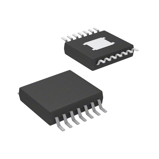
PACKAGE
HTSSOP (14)
BODY SIZE (NOM)
5.00 mm × 4.40 mm
For all available packages, see the package option
addendum at the end of the data sheet.
14
VCC_OUT
Vs = 12 V
Vs = 4.5 V
12
VCC
VCC
+
OPAMP
IN1+
–
IN1–
+
VCC_O1
½
OUT1
ALM2402F-Q1
–
OTF1
GND
Output Voltage (VPP)
•
AEC-Q100 qualified for automotive applications:
– Temperature grade 1: –40°C to +125°C, TA
Functional-Safety Capable
– Documentation available to aid functional safety
system design
Low offset voltage: 1 mV (typical)
High output current drive: 400 mA, continuous (per
channel)
– Replaces discrete op amps and transistors
Wide supply range for both supplies (up to 16 V)
Overtemperature shutdown
Current limit
Shutdown pin for low IQ applications
Stable with large capacitive loads
2-MHz gain bandwidth with 3.4-V/µs slew rate
Internal RF/EMI filter
Package: 14-pin HTSSOP (PWP)
10
8
6
4
2
Simplified Schematic
0
1
10
100
1k
10k
Frequency (Hz)
100k
1M
10M
D013
Maximum Output Voltage vs Frequency
An IMPORTANT NOTICE at the end of this data sheet addresses availability, warranty, changes, use in safety-critical applications,
intellectual property matters and other important disclaimers. PRODUCTION DATA.
�ALM2402F-Q1
www.ti.com
SBOS927B – MAY 2019 – REVISED OCTOBER 2021
Table of Contents
1 Features............................................................................1
2 Applications..................................................................... 1
3 Description.......................................................................1
4 Revision History.............................................................. 2
5 Pin Configuration and Functions...................................3
6 Specifications.................................................................. 4
6.1 Absolute Maximum Ratings........................................ 4
6.2 ESD Ratings............................................................... 4
6.3 Recommended Operating Conditions.........................4
6.4 Thermal Information....................................................5
6.5 Electrical Characteristics: VS = 12 V........................... 5
6.6 Electrical Characteristics: VS = 5 V............................. 6
6.7 Typical Characteristics................................................ 8
7 Detailed Description......................................................14
7.1 Overview................................................................... 14
7.2 Functional Block Diagram......................................... 14
7.3 Feature Description...................................................15
7.4 Device Functional Modes..........................................17
8 Application and Implementation.................................. 18
8.1 Application Information............................................. 18
8.2 Typical Application.................................................... 19
9 Power Supply Recommendations................................23
10 Layout...........................................................................24
10.1 Layout Guidelines................................................... 24
10.2 Layout Example...................................................... 24
11 Device and Documentation Support..........................25
11.1 Documentation Support.......................................... 25
11.2 Receiving Notification of Documentation Updates.. 25
11.3 Support Resources................................................. 25
11.4 Trademarks............................................................. 25
11.5 Electrostatic Discharge Caution.............................. 25
11.6 Glossary.................................................................. 25
12 Mechanical, Packaging, and Orderable
Information.................................................................... 25
4 Revision History
NOTE: Page numbers for previous revisions may differ from page numbers in the current version.
Changes from Revision A (September 2019) to Revision B (October 2021)
Page
• Updated the numbering format for tables, figures, and cross-references throughout the document..................1
• Added functional safety bullets to Features section........................................................................................... 1
Changes from Revision * (May 2019) to Revision A (September 2019)
Page
• Changed device from advanced information (preview) to production data (active)............................................1
2
Submit Document Feedback
Copyright © 2021 Texas Instruments Incorporated
Product Folder Links: ALM2402F-Q1
�ALM2402F-Q1
www.ti.com
SBOS927B – MAY 2019 – REVISED OCTOBER 2021
5 Pin Configuration and Functions
IN(1)±
1
14
GND
IN(1)+
2
13
OUT(1)
OTF/SH_DN
3
12
VS_O(1)
IN(2)+
4
11
VS
Thermal
Pad
IN(2)±
5
10
VS_O(2)
GND
6
9
OUT(2)
NC
7
8
NC
Not to scale
Figure 5-1. PWP (14-Pin HTSSOP) Package, Top View
Table 5-1. Pin Functions
PIN
I/O
DESCRIPTION
NAME
NO.
GND
6, 14
Input
Ground pin (both ground pins must be used and connected together on board)
IN(1)+
2
Input
Noninverting op amp input terminal 1
IN(2)+
4
Input
Noninverting op amp input terminal 2
IN(1)–
1
Input
Inverting op amp input terminal 1
IN(2)–
5
Input
Inverting op amp input terminal 2
7, 8
—
OTF/SH_DN
3
Input/output
OUT(1)
13
Output
Op amp output 1
OUT(2)
9
Output
Op amp output 2
VS
11
Input
Gain stage supply pin
VS_O(1)
12
Input
Output stage supply pin
VS_O(2)
10
Input
Output stage supply pin
Thermal pad
—
—
NC
No internal connection (do no connect)
Overtemperature flag and shutdown (see Table 7-1 for truth table)
Connect the exposed thermal pad to ground for best thermal performance. Do not connect
the thermal pad to any pin other than GND. The thermal pad can also be left floating.
Submit Document Feedback
Copyright © 2021 Texas Instruments Incorporated
Product Folder Links: ALM2402F-Q1
3
�ALM2402F-Q1
www.ti.com
SBOS927B – MAY 2019 – REVISED OCTOBER 2021
6 Specifications
6.1 Absolute Maximum Ratings
over operating free-air temperature range (unless otherwise noted) (1)
MIN
MAX
Input supply voltage, VS = (V+) – (V–)
–0.3
18
V
Output supply voltage, VS_O
–0.3
18
V
Positive and negative input to GND voltage
–0.3
18
V
20
mA
0
7
V
Continuous
Continuous
–40
125
°C
150
°C
150
°C
Overtemperature flag pin current
Overtemperature flag pin voltage
Output
short-circuit(2)
Operating temperature
Junction temperature
Storage temperature, Tstg
(1)
(2)
–65
UNIT
Stresses beyond those listed under Absolute Maximum Ratings may cause permanent damage to the device. These are stress
ratings only, which do not imply functional operation of the device at these or any other conditions beyond those indicated under
Recommended Operating Conditions. Exposure to absolute-maximum-rated conditions for extended periods may affect device
reliability.
Short-circuit to ground; one amplifier per package. Long-term, short-circuit operation leads to an elevated die temperature and a
shorter lifetime, and places the amplifier into open-loop operation. Prolonged open-loop operation (especially at high temperatures and
supplies) can lead to a shift in the dc electrical characteristics, such as offset voltage (see the Open-Loop and Closed-Loop Operation
section).
6.2 ESD Ratings
VALUE
V(ESD)
(1)
Electrostatic discharge
Human-body model (HBM), per AEC Q100-002(1)
HBM ESD Classification Level 2
±2000
Charge Device Model (CDM), per AEC Q100-011
CDM ESD Classification Level C5
±750
UNIT
V
AEC Q100-002 indicates that HBM stressing shall be in accordance with the ANSI/ESDA/JEDEC JS-001 specification
6.3 Recommended Operating Conditions
over operating free-air temperature range (unless otherwise noted)
MIN
Input supply voltage, VS = (V+) – V(–)
Output supply voltage, VS_O
UNIT
3
16
V
400
mA
400
mA
Continous output current (sinking) (1)
1
OTF input low voltage (op amp off or shutdown state)
V
V
0.35
V
Postitive and negative input to GND voltage
0
7
V
Overtemperature flag pin voltage
2
5
V
–40
125
°C
Specified temperature
(1)
4
MAX
16
Continous output current (sourcing) (1)
OTF input high voltage (op amp on or full operational state)
NOM
4.5
Current Limit must be taken into consideration when choosing maximum output current.
Submit Document Feedback
Copyright © 2021 Texas Instruments Incorporated
Product Folder Links: ALM2402F-Q1
�ALM2402F-Q1
www.ti.com
SBOS927B – MAY 2019 – REVISED OCTOBER 2021
6.4 Thermal Information
ALM2402FQ1
THERMAL METRIC(1)
PWP (TSSOP)
UNIT
14 PINS
RθJA
Junction-to-ambient thermal resistance
46.5
°C/W
RθJC(top)
Junction-to-case (top) thermal resistance
33.0
°C/W
RθJB
Junction-to-board thermal resistance
27.6
°C/W
ψJT
Junction-to-top characterization parameter
1.5
°C/W
ψJB
Junction-to-board characterization parameter
27.4
°C/W
RθJC(bot)
Junction-to-case (bottom) thermal resistance
2.2
°C/W
(1)
For more information about traditional and new thermal metrics, see the Semiconductor and IC Package Thermal Metrics application
report.
6.5 Electrical Characteristics: VS = 12 V
at TA = 25°C, VS = VS_O1 = VS_O2 = 12 V, RL = 10 kΩ connected to VS / 2, VCM = VS / 2, VOTF = 5 V, and VO = VS / 2 (unless
otherwise noted)
PARAMETER
TEST CONDITIONS
MIN
TYP
MAX
UNIT
OFFSET VOLTAGE
±1
VOS
Input offset voltage
dVOS/dT
Input offset voltage drift
TA = –40°C to +125°C
PSRR
Input offset voltage versus
power supply
VS = 10 V to 16 V
70
VS = 10 V to 16 V, TA = –40°C to +125°C
65
TA = –40°C to +125°C
±7
±15
65
mV
μV/°C
76
dB
INPUT BIAS CURRENT
IB
Input bias current
IOS
Input offset current
±3.5
TA = –40°C to +125°C
±15
±140
±2
TA = –40°C to +125°C
±12
±35
nA
nA
NOISE
Input voltage noise
f = 0.1 Hz to 10 Hz
eN
Input voltage noise density f = 1 kHz
iN
Input current noise
f = 1 kHz
35
μVPP
5.5
µVRMS
115
nV/√ Hz
20
fA/√ Hz
INPUT VOLTAGE RANGE
VCM
CMRR
Common-mode voltage
VS > 8.2 V
0.2
Common-mode rejection
ratio
0.2 V < VCM < 7 V
81
TA = –40℃ to +125℃, 0.2 V < VCM < 7 V
52
0.3 V < VO < (VS) – 1.5 V,
RL = 10 kΩ
85
7
97
V
dB
OPEN-LOOP GAIN
AOL
Open-loop voltage gain
TA = –40°C to +125°C
93
60
dB
FREQUENCY RESPONSE
GBW
Gain-bandwidth product
CL = 15 pF
2.1
MHz
SR
Slew rate
5-V step, G = +1 V/V, CL = 50 pF
3.4
V/μs
tS
Settling time
To 0.1%, 5-V step , G = +1 V/V
2.4
μs
Overload recovery time
VIN × (–1) × gain > VS
10
μs
Total harmonic distortion +
noise
(V+) = 11 V, (V–) = –5 V, VO = 6 VPP, G = +2 V/V, f = 1
kHz,
RL = 100 Ω
–73
dB
THD+N
Submit Document Feedback
Copyright © 2021 Texas Instruments Incorporated
Product Folder Links: ALM2402F-Q1
5
�ALM2402F-Q1
www.ti.com
SBOS927B – MAY 2019 – REVISED OCTOBER 2021
6.5 Electrical Characteristics: VS = 12 V (continued)
at TA = 25°C, VS = VS_O1 = VS_O2 = 12 V, RL = 10 kΩ connected to VS / 2, VCM = VS / 2, VOTF = 5 V, and VO = VS / 2 (unless
otherwise noted)
PARAMETER
TEST CONDITIONS
MIN
TYP
MAX
TA = 25°C
0.3
0.5
TA = –40°C to +125℃,
ISOURCE = 200 mA
130
300
TA = –40°C to +125℃,
ISOURCE = 100 mA
60
150
TA = 25°C
0.4
0.6
TA = –40°C to +125℃,
ISINK = 200 mA
200
550
TA = –40°C to +125℃,
ISINK = 100 mA
100
200
UNIT
OUTPUT
Positive rail, VID = 100 mV
Voltage output swing from
rail
Vo
Negative rail, VID = 100 mV
ISC
Short-circuit current
Sinking (short to supply)
540
Sourcing (short to ground)
750
mV
mV
mA
POWER SUPPLY
Quiescent current per
amplifier
IQ
IO = 0 A, TA = 25℃
4
IO = 0 A, TA = –40°C to +125°C
5
6
VOTF/SH_DN = 0 V
mA
0.5
TEMPERATURE
Thermal shutdown
165
°C
Thermal shutdown
recovery
159
°C
VOL_OTF
Overtemperature fault low
voltage
VIH_OTF
Amplifier enable voltage
VIL_OTF
Amplifier disable voltage
RPULLUP = 2.5 kΩ, VPULLUP = 5.0 V
400
1
mV
V
0.35
V
6.6 Electrical Characteristics: VS = 5 V
at TA = 25°C, VS = VS_O1 = VS_O2 = 5 V, RL = 10 kΩ connected to VS / 2, VCM = VS / 2, VOTF = 5 V, and VO = VS / 2 (unless
otherwise noted)
PARAMETER
TEST CONDITIONS
MIN
TYP
MAX
UNIT
OFFSET VOLTAGE
VOS
Input offset voltage
dVOS/dT
Input offset voltage drift
Input offset voltage versus
power supply
PSRR
TA = 25°C
±1
TA = –40°C to +125°C
±7
±15
TA = –40°C to +125°C
65
VS = 4.5 V to 10 V
82
VS = 4.5 V to 10 V,
TA = –40°C to +125°C
75
mV
μV/°C
94
dB
INPUT BIAS CURRENT
IB
Input bias current
IOS
Input offset current
TA = 25°C
0.5
TA = –40°C to +125°C
TA = 25°C
±2
±30
±2
TA = –40°C to +125°C
±2
±9
nA
nA
NOISE
Input voltage noise
6
f = 0.1 Hz to 10 Hz
eN
Input voltage noise density f = 1 kHz
iN
Input current noise
f = 1 kHz
Submit Document Feedback
35
μVPP
5.5
µVRMS
115
nV/√ Hz
20
fA/√ Hz
Copyright © 2021 Texas Instruments Incorporated
Product Folder Links: ALM2402F-Q1
�ALM2402F-Q1
www.ti.com
SBOS927B – MAY 2019 – REVISED OCTOBER 2021
6.6 Electrical Characteristics: VS = 5 V (continued)
at TA = 25°C, VS = VS_O1 = VS_O2 = 5 V, RL = 10 kΩ connected to VS / 2, VCM = VS / 2, VOTF = 5 V, and VO = VS / 2 (unless
otherwise noted)
PARAMETER
TEST CONDITIONS
MIN
TYP
MAX
UNIT
INPUT VOLTAGE RANGE
VCM
CMRR
Common-mode voltage
Common-mode rejection
ratio
0.2
0.2 V < VCM < (V+) – 1.2 V
80
TA = –40℃ to +125℃,
0.2 V < VCM < (V+) – 1.2 V
52
(V+) – 1.2
V
95
dB
OPEN-LOOP GAIN
AOL
Open-loop voltage gain
0.3 V < VO < (VS) – 1.5 V,
RL = 10 kΩ
TA = 25°C
85
TA = –40°C to +125°C
60
93
dB
FREQUENCY RESPONSE
GBW
Gain-bandwidth product
CL = 15 pF
1.3
MHz
SR
Slew rate
2-V step, G = +1 V/V,
CL = 50 pF
1.7
V/μs
tS
Settling time
To 0.1%, 2-V step , G = +1 V/V
2
μs
Overload recovery time
VIN × (–1) × gain > VS
5
μs
Total harmonic distortion +
noise
VS = 5 V, VO = 2.82 VPP, G = +2 V/V,
f = 1 kHz, RL = 100 Ω
–73
dB
THD+N
OUTPUT
Positive rail, VID = 100 mV
Vo
Voltage output swing from
rail
Negative rail, VID = 100 mV
ISC
Short-circuit current
TA = 25°C
0.3
0.5
TA = –40°C to +125℃,
ISINK = 200 mA
130
300
TA = –40°C to +125℃,
ISINK = 100 mA
60
150
TA = 25°C
0.4
0.6
TA = –40°C to +125℃,
ISINK = 200 mA
200
575
TA = –40°C to +125℃,
ISINK = 100 mA
100
200
Sinking (short to supply)
500
Sourcing (short to ground)
550
mV
mV
mA
POWER SUPPLY
IQ
Quiescent current per
amplifier
IO = 0 A, TA = 25℃
4
IO = 0 A, TA = –40°C to +125°C
4.5
5
VOTF/SH_DN = 0 V
mA
0.5
TEMPERATURE
Thermal shutdown
165
°C
Thermal shutdown
recovery
159
°C
VOL_OTF
Overtemperature fault low
voltage
VIH_OTF
Amplifier enable voltage
VIL_OTF
Amplifier disable voltage
RPULLUP = 2.5 kΩ, VPULLUP = 5.0 V
400
1
mV
V
0.35
V
Submit Document Feedback
Copyright © 2021 Texas Instruments Incorporated
Product Folder Links: ALM2402F-Q1
7
�ALM2402F-Q1
www.ti.com
SBOS927B – MAY 2019 – REVISED OCTOBER 2021
6.7 Typical Characteristics
at TA= 25°C, VS = 12 V, VCM= VS_O1= VS_O2= VS/2, and RL= 10 kΩ (unless otherwise noted)
40
30
36
Offset Voltage (mV)
28
Amplifiers (%)
40 qC
20
32
24
20
16
12
8
25 qC
10
0
-10
-20
125 qC
4
-120
-100
-80
-60
-40
Offset Voltage Drift (µV/qC)
-20
-30
-6
0
-5
D001
-4
-3
-2
-1
0
Input Common-mode Voltage (V)
1
2
D017
5 typical units
Figure 6-2. Offset Voltage
vs Input Common-Mode Voltage
Figure 6-1. Offset Voltage Drift
Production Distribution
120
5
4
100
180
Gain
Phase 150
80
120
60
90
40
60
20
30
0
0
1
0
-1
-2
Phase (q)
2
Gain (dB)
Offset Voltage (mV)
3
-3
-4
-5
4
6
8
10
12
Supply Voltage (V)
14
16
-20
100m
10
D018
CLOAD = 200 nF
5 typical units
100
1k
10k
Frequency (Hz)
100k
1M
-30
10M
D002
RL = 50 Ω
Figure 6-4. Open-Loop Gain and Phase
vs Frequency
Figure 6-3. Offset Voltage vs Power Supply
30
65
G= 1
G= 1
G = 10
VS = 12 V
VS = 4.5 V
60
20
55
50
Gain (dB)
Phase Margin (q)
1
45
40
10
0
35
30
-10
25
20
10
100
Load Capacitance (pF)
1000
-20
100
D003
1k
10k
100k
Frequency (Hz)
1M
10M
D004
Gain = 1 V/V
Figure 6-5. Phase Margin vs Capacitive Load
8
Figure 6-6. Closed-Loop Gain vs Frequency
Submit Document Feedback
Copyright © 2021 Texas Instruments Incorporated
Product Folder Links: ALM2402F-Q1
�ALM2402F-Q1
www.ti.com
SBOS927B – MAY 2019 – REVISED OCTOBER 2021
6.7 Typical Characteristics (continued)
at TA= 25°C, VS = 12 V, VCM= VS_O1= VS_O2= VS/2, and RL= 10 kΩ (unless otherwise noted)
100
120
VS = 12 V
VS = 4.5 V
100
60
40
20
80
60
40
20
0
0
1
10
100
1k
10k
Frequency (Hz)
100k
1M
10M
1
10
D005
Figure 6-7. PSRR vs Frequency
-40
-60
0.01
-80
D006
0.1
-60
0.01
-80
10k
-100
100m
1
Output Amplitude (VRMS)
D010
D011
Input signal
Measurement
frequency =1 kHz bandwidth = 80 kHz
Measurement
bandwidth = 80 kHz
Figure 6-10. THD+N vs Output Amplitude
Figure 6-9. THD+N Ratio vs Frequency
14
32
Vs = 12 V
Vs = 4.5 V
24
Input Bias Current (nA)
12
Output Voltage (VPP)
10M
-40
0.001
10m
-100
0.001
Gain = 2 V/V
1M
RLOAD = 100 :
RLOAD = 10K :
Noise (%)
Total Harmonic Distortion
Noise (dB)
0.1
VO = 8 VPP
100k
1
Total Harmonic Distortion
Total Harmonic Distortion
Noise ( )
RLOAD = 100 :
RLOAD = 10K :
1k
Frequency (Hz)
1k
10k
Frequency (Hz)
Figure 6-8. CMRR vs Frequency
1
100
100
Total Harmonic Distortion + Noise (dB)
Rejection Ratio (dB)
80
, VS = 12 V
, VS = 12 V
, VS = 4.5 V
, VS = 4.5 V
Rejection Ratio (dB)
PSRR
PSRR
PSRR
PSRR
10
8
6
4
IB +
16
IB
8
0
IOS
-8
2
0
1
10
100
1k
10k
Frequency (Hz)
100k
1M
10M
-16
-6
-4.5
D013
Figure 6-11. Maximum Output Voltage
vs Frequency
-3
-1.5
0
1.5
Input Common-mode Voltage (V)
3
D019
Figure 6-12. Input Bias Current
vs Common-Mode Voltage
Submit Document Feedback
Copyright © 2021 Texas Instruments Incorporated
Product Folder Links: ALM2402F-Q1
9
�ALM2402F-Q1
www.ti.com
SBOS927B – MAY 2019 – REVISED OCTOBER 2021
6.7 Typical Characteristics (continued)
45
5
40
4.5
35
4
30
Output Voltage (V)
Input Bias Current (nA)
at TA= 25°C, VS = 12 V, VCM= VS_O1= VS_O2= VS/2, and RL= 10 kΩ (unless otherwise noted)
IB
25
20
IB +
15
10
IOS
3.5
25 qC
3
85 qC
2.5
125 qC
2
1.5
5
1
0
0.5
-5
-40
40 qC
0
-20
0
20
40
60
80
Temperature (qC)
100
120
0
140
0.2
D020
0.4
0.6
Output Current (A)
0.8
1
D022
Figure 6-14. Output Voltage Swing
vs Output Source Current
Figure 6-13. Input Bias Current vs Temperature
130
0
125
120
Rejection Ratio (dB)
Output Voltage (V)
-1.5
85 qC
40 qC
-3
125 qC
-4.5
25 qC
115
110
105
100
95
90
85
80
75
-6
0
0.2
0.4
Output Current (A)
0.6
70
-40
0.8
Figure 6-15. Output Voltage Swing
vs Output Sink Current
20
40
60
80
Temperature (qC)
100
120
140
D025
Input Referred Voltage Noise (10 PV/div)
Power Supply Rejection Ratio (dB)
92
90
88
86
84
82
80
78
76
74
72
-20
0
20
40
60
80
Temperature (qC)
100
120
Time (1 s/div)
140
D027
D026
Figure 6-17. PSRR vs Temperature
10
0
Figure 6-16. CMRR vs Temperature
94
70
-40
-20
D024
Figure 6-18. 0.1-Hz to 10-Hz Noise
Submit Document Feedback
Copyright © 2021 Texas Instruments Incorporated
Product Folder Links: ALM2402F-Q1
�ALM2402F-Q1
www.ti.com
SBOS927B – MAY 2019 – REVISED OCTOBER 2021
6.7 Typical Characteristics (continued)
at TA= 25°C, VS = 12 V, VCM= VS_O1= VS_O2= VS/2, and RL= 10 kΩ (unless otherwise noted)
3.5
Quiescent Current Per Amplifer (mA)
Voltage Noise Density (nV/—Hz)
10000
1000
100
10
3
2.5
2
1.5
1
0.5
0
5
100m
1
10
100
1k
Frequency (Hz)
10k
100k
0
1M
2
4
6
8
10
Supply Voltage (V)
D007
5 typical units
90
4.5
85
3.5
3
2.5
VS = 4.5 V
2
D028
VS = 12 V
75
70
65
60
VS = 4.5 V
55
1.5
50
1
-40
-20
0
20
40
60
80
Temperature (qC)
100
120
45
-40
140
-20
0
D029
5 typical units
20
40
60
80
Temperature (qC)
100
120
140
D030
RL = 100 Ω
Figure 6-21. Quiescent Current vs Temperature
Figure 6-22. Open-Loop Gain vs Temperature
100000
30
25
10000
RISO = 0
RISO = 25
RISO = 50
20
Overshoot ( )
ZOUT (:)
16
VO = 8 VPP
80
Open-Loop Gain (dB)
Quiescent Current (mA)
5
VS = 16 V
14
Figure 6-20. Quiescent Current vs Power Supply
Figure 6-19. Input Voltage Spectral Noise Density vs Frequency
4
12
1000
15
10
5
100
0
10
100m
1
10
100
1k
10k
Frequency (Hz)
100k
1M
10M
-5
10
100
Capactiance (pF)
D012
10-mV output step
Figure 6-23. Open-Loop Output Impedance
vs Frequency
1000
D032
Gain = –1 V/V
Figure 6-24. Small-Signal Overshoot
vs Capacitive Load
Submit Document Feedback
Copyright © 2021 Texas Instruments Incorporated
Product Folder Links: ALM2402F-Q1
11
�ALM2402F-Q1
www.ti.com
SBOS927B – MAY 2019 – REVISED OCTOBER 2021
6.7 Typical Characteristics (continued)
at TA= 25°C, VS = 12 V, VCM= VS_O1= VS_O2= VS/2, and RL= 10 kΩ (unless otherwise noted)
50
Voltage (2 V/div)
Overshoot ( )
40
VIN (V), VS = 12 V
VOUT (V), VS = 12 V
VIN (V), VS = 4.5 V
VOUT (V), VS = 4.5 V
RISO = 0
RISO = 25
RISO = 50
30
20
10
0
10
100
Capactiance (pF)
10-mV output step
1000
Time (100 Ps/div)
D033
D034
Gain = 1 V/V
Figure 6-25. Small-Signal Overshoot
vs Capacitive Load
Figure 6-26. No Phase Reversal
Voltage (1 V/div)
Voltage (5 mV/div)
VIN
VOUT, RLOAD = 10K :
VOUT, RLOAD = 50 :
VOUT
VIN
Time (5 Ps/div)
Time (1 Ps/div)
D035
D036
VS = 4.5 V
VIN = 10 mVPP
Figure 6-27. Negative Overload Recovery
Figure 6-28. Small-Signal Step Response
0.9
Faling
Rising
0.85
Output (5 mV/div)
Short-Circuit Current (A)
0.8
Sourcing
0.75
0.7
0.65
0.6
0.55
0.5
Sinking
0.45
0.4
0.35
-40
Time (1 Ps/div)
-20
D040
0
20
40
60
80
Temperature (qC)
100
120
140
D041
VIN = 5 V
Figure 6-29. Settling Time
12
Figure 6-30. Short-Circuit Current vs Temperature
Submit Document Feedback
Copyright © 2021 Texas Instruments Incorporated
Product Folder Links: ALM2402F-Q1
�ALM2402F-Q1
www.ti.com
SBOS927B – MAY 2019 – REVISED OCTOBER 2021
6.7 Typical Characteristics (continued)
EMIRR IN+ (dB)
at TA= 25°C, VS = 12 V, VCM= VS_O1= VS_O2= VS/2, and RL= 10 kΩ (unless otherwise noted)
160
150
140
130
120
110
100
90
80
70
60
50
40
30
20
10
0
10M
100M
1G
Frequency (Hz)
10G
D015
PRF = –10 dBm
Figure 6-31. EMIRR vs Frequency
Submit Document Feedback
Copyright © 2021 Texas Instruments Incorporated
Product Folder Links: ALM2402F-Q1
13
�ALM2402F-Q1
www.ti.com
SBOS927B – MAY 2019 – REVISED OCTOBER 2021
7 Detailed Description
7.1 Overview
The ALM2402F-Q1 is a dual-power op amp qualified for use in automotive applications. Key features for this
device are low offset voltage, high output current drive capability, and high FPBW capability. The device also
offers protection features such as thermal shutdown and current limit. The 14-pin HTSSOP package minimizes
board space and power dissipation.
7.2 Functional Block Diagram
VCC
IN(1)+
EMI
VS_O(1)
13
OUT(1)
14
GND
11
VS
10
VS_O(2)
9
OUT(2)
PMOS Current Limiting and
Biasing
+
2
12
OTA
Rejection
IN(1)±
NMOS Current Limiting and
Biasing
±
1
EN
EN
OTF/SH_DN
3
VCC
Internal
Thermal Detection
Circuitry
VCC
IN(2)+
PMOS Current Limiting and
Biasing
+
4
EMI
OTA
Rejection
14
IN(2)±
5
GND
6
NMOS Current Limiting and
Biasing
±
EN
Submit Document Feedback
Copyright © 2021 Texas Instruments Incorporated
Product Folder Links: ALM2402F-Q1
�ALM2402F-Q1
www.ti.com
SBOS927B – MAY 2019 – REVISED OCTOBER 2021
7.3 Feature Description
7.3.1 OTF/SH_DN
The overtemperature and shutdown (OTF/SH_DN) pin is a bidirectional pin that allows both op amps to be put
into a low IQ state (~500 µA) when forced low or less than VIL_OTF. As a result of this pin being bidirectional, and
the respective enable and disable functionality, this pin must be pulled high or greater than VIH_OTF through a
pullup resistor; see the Electrical Characteristics table.
When the junction temperature of ALM2402F-Q1 exceeds the limits specified in the Recommended Operating
Conditions table, the OTF/SH_DN pin goes low to alert the application that both the outputs have turned off
because of an overtemperature event. Also, the OTF pin goes low if VS_O1 and VS_O2 are 0 V. In case of an
overtemperature event, the op amps are shut down even if OTF/SH_DN is forced high.
When OTF/SH_DN is pulled low and the op amps are shut down, the op amps are in an open loop, even when
there is negative feedback applied. This occurrence is due to the loss of the open-loop gain in the op amps when
the biasing is disabled. See Section 7.4.1 for more details on open- and closed-loop considerations.
7.3.2 Output Stage Supply Voltage
The ALM2402F-Q1 uses three power rails. VS powers the op-amp signal path (OTA) and protection circuitry.
VS_O1 and VS_O2 power the output high side driver. Each supply can operate at separate voltage levels
(higher or lower). The minimum and maximum values listed in the Recommended Operating Conditions table
are voltages that enable the ALM2402F-Q1 to properly function at or near the specification listed in Electrical
Characteristics table.
7.3.3 Current-Limit and Short-Circuit Protection
Each op amp in the ALM2402F-Q1 has separate internal current limiting for the PMOS (high-side) and NMOS
(low-side) output transistors. If the output is shorted to ground then the PMOS (high-side) current limit is
activated, and limits the current to 750 mA nominally. If the output is shorted to supply then the NMOS
(low-side) current limit is activated and limits the current to 550 mA nominally at 25°C. The current limit value
decreases with increasing temperature as a result of the temperature coefficient of a base-emitter junction
voltage. Similarly, the current limit value increases at low temperatures.
In the case of short-to-ground scenarios, a programmable current limit for the PMOS (high-side) is achieved
by adding resistance between VS_O(x), where x = 1 or 2, and the supply VS. The added current limit resistor
reduces the drain-source voltage across the PMOS output transistor, thus reducing the output current drive
capability. For a desired current limit (ILIMIT), an appropriate current limiting resistor (Rlimit) is selected using
Equation 1.
RLIMIT
(VS 1.5) / ILIMIT
(1)
When current is limited, the safe limits for the die temperature must be taken in to account; see the
Recommended Operating Conditions and Absolute Maximum Ratings tables. With too much power dissipation,
the die temperature can surpass thermal shutdown limits; the op amp shuts down and reactivates after the die
has fallen below thermal limits. However, do not continuously operate the device in thermal hysteresis for long
periods of time (see the Absolute Maximum Ratings table).
Submit Document Feedback
Copyright © 2021 Texas Instruments Incorporated
Product Folder Links: ALM2402F-Q1
15
�ALM2402F-Q1
www.ti.com
SBOS927B – MAY 2019 – REVISED OCTOBER 2021
7.3.4 Input Common-Mode Overvoltage Clamps
The input common mode range of the ALM2402F-Q1 is between (V–) + 0.2 V and (V+) – 1.2 V (see the
Electrical Characteristics table). Staying within this range allows the op amps to perform and operate within
the specification listed in the Electrical Characteristics. Operating beyond these limits can cause distortion and
nonlinearities.
In order for the inputs to tolerate high voltages in the event of a short to supply, Zener diodes have been added
(see Figure 7-1). The current into this Zener diode is limited through internal resistors (10 kΩ each). When
operating near or above the Zener voltage (7 V), the additional voltage error caused by the mismatch in internal
resistors must be taken in to account. In unity gain configurations, the op amp forces both gate voltages to be
equal to the Zener voltage on the positive input pin, and ideally both Zeners sink the same amount of current and
force the output voltage to be equal to VIN. However, in reality, RN and RP and VZ between both Zener diodes
do not perfectly match, and have some percentage difference between their values. This occurrence leads to the
output being VO = VIN × (ΔR + ΔVZ) .
½
ALM2402F-Q1
RN
–
+
RP
+
VIN
–
Figure 7-1. Schematic Including Input Clamps
7.3.5 Thermal Shutdown
If the die temperature exceeds safe limits, all outputs are disabled, and the OTF/SH_DN pin is driven low. After
the die temperature has fallen to a safe level, operation automatically resumes. The OTF/SH_DN pin is released
after operation has resumed.
When operating the die at a high temperature, the op amp toggles on and off between the thermal shutdown
hysteresis. In this event, the safe limits for the die temperature must be taken in to account; see the
Recommended Operating Conditions and Thermal Conditions tables. Do not continuously operate the device
in thermal hysteresis for long periods of time; see the Recommended Operating Conditions table.
16
Submit Document Feedback
Copyright © 2021 Texas Instruments Incorporated
Product Folder Links: ALM2402F-Q1
�ALM2402F-Q1
www.ti.com
SBOS927B – MAY 2019 – REVISED OCTOBER 2021
7.3.6 Output Stage
Designed as a high-voltage, high current operational amplifier, the ALM2402F-Q1 device delivers a robust output
drive capability. A class AB output stage with common-source transistors is used to achieve full rail-to-rail output
swing capability. For resistive loads up to 10 kΩ, the output swings typically to within 5 mV of either supply rail
regardless of the power-supply voltage applied. Different load conditions change the ability of the amplifier to
swing close to the rails.
Each output transistor has internal reverse diodes between drain and source that conduct if the output is forced
greater than the supply or less than ground (reverse current flow). These diodes can be used as flyback
protection in inductive-load driving applications. Limit the use of these diodes to pulsed operation to minimize
junction temperature overheating due to (VF × IF). Internal current limiting circuitry does not operate when current
is flown in the reverse direction and the reverse diodes are active.
7.3.7 EMI Susceptibility and Input Filtering
Op amps vary with regard to the susceptibility of the device to electromagnetic interference (EMI). If conducted
EMI enters the op amp, the dc offset observed at the amplifier output may shift from the nominal value while EMI
is present. This shift is a result of signal rectification associated with the internal semiconductor junctions. While
all op-amp pin functions can be affected by EMI, the signal input pins are likely to be the most susceptible. The
ALM2402F-Q1 incorporates an internal input low-pass filter that reduces the amplifiers response to EMI. Both
common-mode and differential mode filtering are provided by this filter.
Texas Instruments has developed the ability to accurately measure and quantify the immunity of an operational
amplifier over a broad frequency spectrum extending from 10 MHz to 990 MHz. The EMI rejection ratio (EMIRR)
metric allows op amps to be directly compared by the EMI immunity. Detailed information can also be found in
the EMI Rejection Ratio of Operational Amplifiers application report, available for download from www.ti.com.
7.4 Device Functional Modes
7.4.1 Open-Loop and Closed-Loop Operation
As a result of the very high open-loop dc gain of the ALM2402F-Q1, the device functions as a comparator
in open-loop for most applications. As noted in the Electrical Characteristics table, the majority of electrical
characteristics are verified in negative feedback, closed-loop configurations. Certain dc electrical characteristics,
like offset, may have a higher drift across temperature and lifetime when continuously operated in open loop
over the lifetime of the device.
7.4.2 Shutdown
When the OTF/SH_DN pin is left floating or is grounded, the op amp shuts down to a low IQ state and does
not operate; the op amp outputs go to a high-impedance state. See the OTF/SH_DN section for more detailed
information on the OTF/SH_DN pin.
Table 7-1. Shutdown Truth Table
NAME
OTF/SH_DN
LOGIC STATE
OP AMP STATE
High ( > VIH_OTF see Recommended Operating Conditions)
Operating
Low ( < VIL_OTF see Recommended Operating Conditions)
Shutdown (low IQ state)
Submit Document Feedback
Copyright © 2021 Texas Instruments Incorporated
Product Folder Links: ALM2402F-Q1
17
�ALM2402F-Q1
www.ti.com
SBOS927B – MAY 2019 – REVISED OCTOBER 2021
8 Application and Implementation
Note
Information in the following applications sections is not part of the TI component specification,
and TI does not warrant its accuracy or completeness. TI’s customers are responsible for
determining suitability of components for their purposes, as well as validating and testing their design
implementation to confirm system functionality.
8.1 Application Information
The ALM2402F-Q1 is a dual-power op amp with performance and protection features that are optimal for many
applications. For op amps, there are many general design consideration that must taken into account. The
following sections describe what to consider for most closed-loop applications, and gives a specific example of
the ALM2402F-Q1 being used in a motor-drive application.
8.1.1 Capacitive Load and Stability
The ALM2402F-Q1 is designed to be used in applications where driving a capacitive load is required. As
with all op amps, specific instances can occur where the ALM2402F-Q1 device can become unstable. The
particular op-amp circuit configuration, layout, gain, and output loading are some of the factors to consider
when establishing whether or not an amplifier is stable in operation. An op amp in the unity-gain (1 V/V) buffer
configuration that drives a capacitive load exhibits a greater tendency to be unstable than an amplifier operated
at a higher-noise gain. The capacitive load, in conjunction with the op-amp output resistance, creates a pole
within the feedback loop that degrades the phase margin. The degradation of the phase margin increases as
the capacitive loading increases. When operating in the unity-gain configuration, the ALM2402F-Q1 remains
stable with a pure capacitive load up to approximately 1 nF. Increasing the amplifier closed-loop gain allows
the amplifier to drive increasingly larger capacitance. This increased capability is evident when observing the
overshoot response of the amplifier at higher voltage gains.
One technique for increasing the capacitive load drive capability of the amplifier operating in a unity-gain
configuration is to insert a small resistor, typically 100 mΩ to 10 Ω, in series with the output (RS), as shown in
Figure 8-1. This resistor significantly reduces the overshoot and ringing associated with large capacitive loads.
V+
±
RS
VOUT
+
VIN
+
±
RL
CL
Figure 8-1. Capacitive Load Drive
18
Submit Document Feedback
Copyright © 2021 Texas Instruments Incorporated
Product Folder Links: ALM2402F-Q1
�ALM2402F-Q1
www.ti.com
SBOS927B – MAY 2019 – REVISED OCTOBER 2021
8.2 Typical Application
R2
R1
Resolver
+
COSINE
Sensing
Coil
Rotor
Excitation
Coil
Vbias
ALM2402F-Q1
+
SINE
CBL
R3
Sensing
Coil
R4
SIN+
SIN–
COS–
COS+
CBL
V+
excite–
V–
V+
excite+
DAC
ADC
ADC
V–
Resolver-to-Digital
Converter
Figure 8-2. Resolver-Based Application
High-power ac and brushless DC (BLDC) motor-drive applications need angular and position feedback in order
to efficiently and accurately drive the motor. Position feedback can be achieved by using optical encoders,
hall sensors, or resolvers. Resolvers are the goto choice when environmental or longevity requirements are
challenging and extensive.
A resolver acts like a transformer with one primary coil and two secondary coils. The primary coil, or excitation
coil, is located on the rotor of the resolver. As the rotor of the resolver spins, the excitation coil induces a current
into the sine and cosine sensing coils. These coils are oriented 90 degrees from one another, and produce a
vector position read by the resolver to digital converter chip.
Resolver excitation coils can have a very low dc resistance (< 100 Ω), requiring a sink and a source of up to 200
mA from the excitation driver. The ALM2402F-Q1 can source and sink this current while providing current limiting
and thermal shutdown protection. Incorporating these protections in a resolver design can increase the life of the
end product.
The fundamental design steps and ALM2402F-Q1 benefits shown in this application example can be applied to
other inductive load applications, such as dc and servo motors.
Submit Document Feedback
Copyright © 2021 Texas Instruments Incorporated
Product Folder Links: ALM2402F-Q1
19
�ALM2402F-Q1
www.ti.com
SBOS927B – MAY 2019 – REVISED OCTOBER 2021
8.2.1 Design Requirements
For this design example, use the parameters listed in Table 8-1 as the input parameters.
Table 8-1. Design Parameters
DESIGN PARAMETER
EXAMPLE VALUE
Ambient temperature range
–40°C to +125°C
Available supply voltages
12 V
EMC capacitance (CL)
50 nF
Excitation input voltage range
2 VRMS to 7 VRMS
Excitation frequency
10 kHz
8.2.2 Detailed Design Procedure
When using the ALM2402F-Q1 in a resolver application, determine:
•
•
•
•
•
•
Resolver excitation input impedance or resistance and inductance: ZO= 100 + j188; (R = 100 Ω and L = 3
mH)
Resolver transformation ration (VEXC / VSINCOS): 0.5 V/V at 10 kHz
Package and RθJA: HTSSOP, 46.5°C/W
Op amp maximum junction temperature: 150°C
Op amp bandwidth: 1.3 MHz
Op amp Slew Rate: 1.2 V/µs
8.2.2.1 Resolver Excitation Input (Op Amp Output)
Like a transformer, a resolver needs an alternating current input to function properly. The resolver receives
alternating current from the primary coil (excitation input) and creates a multiple of this input current on the
secondary sides (SIN, COS ports). When determining how to generate this alternating current, make sure to
understand the op amp abilities and limitations. For the excitation input, the resolver input impedance, stability
RMS voltage, and desired frequency must be taken in to account.
8.2.2.1.1 Excitation Voltage
The resolver primary winding or excitation coil can be driven by a single-ended op amp output with the other side
of the coil grounded, or differentially as shown in Figure 8-2. A differential drive offers higher voltage (double)
on to the excitation coil, while not using as much output voltage headroom from the op amp. This larger output
voltage due to the differential drive leads to lower distortion on the output signal.
For this example, the resolver impedance is specified from 2 VRMS and 7 VRMS up to 20-kHz maximum
frequency. To highlight use with a 7 VRMS resolver, an excitation voltage of 10 VPP is applied from each
channel of the ALM2402F-Q1. The op amp is set in an inverting gain = –2 V/V, while applying an adequate
common-mode bias. These conditions give the required 7 VRMS differential output (3.5 VRMS per each op amp
channel) to the resolver primary winding without running into any op-amp headroom issues.
Another consideration for excitation is op-amp power dissipation. As described in the Power Dissipation and
Thermal Reliability section, power dissipation from the op amp can be lowered by driving the output peak
voltages close to the supply and ground voltages. With the very low VOH/VOL of the ALM2402F-Q1, lower power
dissipation is easily accomplished. See the Output Stage section for a further description of the rail-rail output
stage.
8.2.2.1.2 Excitation Frequency
The excitation frequency is chosen based on the desired secondary-side output signal resolution. The excitation
signal is similar to a sampling pulse in ADCs, with the real information being in the envelope created by the rotor.
With a GBW of 1.3 MHz, the ALM2402F-Q1 has more than enough open-loop gain at 10 kHz to create negligible
closed-loop gain error.
Along with GBW, the ALM2402F-Q1 has optimal THD and SR performance to achieve 10-VPP output per
channel.
20
Submit Document Feedback
Copyright © 2021 Texas Instruments Incorporated
Product Folder Links: ALM2402F-Q1
�ALM2402F-Q1
www.ti.com
SBOS927B – MAY 2019 – REVISED OCTOBER 2021
8.2.2.1.3 Excitation Impedance
Knowledge of the primary-side impedance is very important when choosing an op amp for this application. As
shown in Figure 8-3, the excitation coil looks like an inductance in series with a resistance. Often, these values
are not given, or are given as a function of frequency or phase angle, and must by calculated from the Cartesian
or polar form. This calculation is a trivial task.
After the coil resistance is determined, the maximum or peak-peak current needed from ALM2402F-Q1 is
determined using Equation 2:
IOUT =
VPP
RL
(2)
In this example, the peak-to-peak output current equates to approximately 100 mA. Each op amp handles the
peak current, with one op amp sinking current while the other op amp is sourcing current. Knowledge of the op
amp current is very important when determining the device power dissipation, a topic that is discussed in Power
Dissipation and Thermal Reliability.
R2
CEMC
Excitation Coil
Model
R1
–
+
LEXC
RCRS
ALM2402F-Q1
RL
Vbias
CCRS
+
–
R3
CEMC
R4
Figure 8-3. Excitation Coil Implementation
As shown in Figure 8-3, designers often add a resistor (RCRS) in series with a capacitor (CCRS) to eliminate
crossover distortion. This distortion occurs as a result of the biasing of BJTs in a discrete implementation. With
the ALM2402F-Q1 rail-rail output and high-output current drive capability, this configuration is rarely needed.
Common practice is to also add EMC capacitors to the op-amp outputs to help shield other devices on the PCB
from the radiation created by the motor and resolver. When choosing CEMC, make sure to take the stability of the
op amp into account.
8.2.2.2 Resolver Output
As mentioned in Section 8.2.2.1.2, the excitation signal is similar to a sampling pulse in ADCs, with the real
information being in the envelope created by the rotor. Equation 3, Equation 4, and Equation 5 show the
behavior of the sin and cos outputs. The excitation signal is attenuated and enveloped by the voltage created
from the electromagnetic response of the rotating rotor. The resolver analog-output-to-digital converter filters out
the excitation signal, and processes the sine and cosine angles produced by the rotor. Hence, signal integrity or
Submit Document Feedback
Copyright © 2021 Texas Instruments Incorporated
Product Folder Links: ALM2402F-Q1
21
�ALM2402F-Q1
www.ti.com
SBOS927B – MAY 2019 – REVISED OCTOBER 2021
the sine and cosine envelope is most important in resolver design; although, some trade-offs in signal integrity of
the excitation signal can be made for cost or convenience. Often, a square wave or sawtooth signal is used to
accomplish excitation, as opposed to a sine wave.
VEXC = VPP u sin(2Sft)
(3)
VSIN = TR u VPP u sin(2Sft) u sin(T)
(4)
VCOS = TR u VPP u sin(2Sft) u cos(T)
(5)
8.2.2.3 Power Dissipation and Thermal Reliability
Power dissipation is critical to many industrial and automotive applications. Resolvers are typically chosen
over other position feedback techniques because of reliability and accuracy in harsh conditions and high
temperatures.
The ALM2402F-Q1 is capable of high output current with power-supply voltages up to 16 V. Internal power
dissipation increases when operating at high supply voltages. The power dissipated in the op amp (POPA) is
calculated using Equation 6:
POPA
(V
VO(X)) u IOUT
(V
VO(X)) u
VO(X)
RL
(6)
To calculate the worst-case power dissipation in the op amp, the ac and dc cases must be considered
separately.
In the case of constant output current (dc) to a resistive load, the maximum power dissipation in the op amp
occurs when the output voltage is half the positive supply voltage. This calculation assumes that the op amp is
sourcing current from the positive supply to a grounded load. If the op amp sinks current from a grounded load,
modify Equation 7 to include the negative supply voltage instead of the positive.
POPA(MAX _ DC)
POPA (
VO(X)
)
2
(VO(X))2
4RL
(7)
The maximum power dissipation in the op amp for a sinusoidal output current (ac) to a resistive load occurs
when the peak output voltage is 2/π times the supply voltage, given symmetrical supply voltages, as shown in
Equation 8:
POPA(MAX _ AC)
POPA (
2VO(X)
)
S
2 ˜ (VO(X))2
S2 ˜ RL
(8)
After the total power dissipation is determined, the junction temperature at the worst expected ambient
temperature case must be determined by using Equation 9:
TJ(MAX) = POPA u RTJA
TA(MAX)
(9)
8.2.2.3.1 Improving Package Thermal Performance
The value of RθJA depends on the PCB layout. An external heat sink, a cooling mechanism such as a cold air
fan, or both, can help reduce RθJA and thus improve device thermal capabilities. See TI’s design support web
page at www.ti.com/thermal for general guidance on improving device thermal performance.
22
Submit Document Feedback
Copyright © 2021 Texas Instruments Incorporated
Product Folder Links: ALM2402F-Q1
�ALM2402F-Q1
www.ti.com
SBOS927B – MAY 2019 – REVISED OCTOBER 2021
8.2.3 Application Curves
The THD+N performance for the circuit described in the Excitation Voltage section is measured for a 10-kHz,
10-VPP output signal from each op-amp channel. These measurement results are displayed in Table 8-2.
Table 8-2. Maximum Output Power and THD+N
LOAD IMPEDANCE
(Ω)
MAXIMUM OUTPUT POWER
(mW)
THD+N AT MAXIMUM OUTPUT POWER
(dB)
100
292
–50
Figure 8-4 shows the THD+N performance for different input signal frequencies with a measurement bandwidth
of 80 kHz. Figure 8-5 shows the circuit response with load capacitances of up to 100 nF. Using a larger resistor
in series with the output, as shown in Section 8.1.1 further improves phase margin.
1
Noise (dB)
100
-60
-80
0.01
90
80
Overshoot ( )
0.1
Total Harmonic Distortion
Noise ( )
Total Harmonic Distortion
-40
G 1
G 2
100
1k
Frequency (Hz)
70
60
50
40
30
20
10
10
-100
0.001
RISO = 0
RISO = 5
RISO = 10
10k
D044
Figure 8-4. THD+N vs Frequency
100
1000
Capactiance (pF)
10000
100000
D043
Figure 8-5. Small-Signal Overshoot vs Capacitive
Load
9 Power Supply Recommendations
The ALM2402F-Q1 is specified for continuous operation from 4.5 V to 16 V (±2.25 V to ±8 V) for VS, and 3 V to
16V (±1.5 V to ±8 V) for VS_O(X); many specifications apply from –40°C to +125°C.
Place 0.1-μF bypass capacitors close to the power-supply pins to reduce errors coupling in from noisy or
high-impedance power supplies. For more detailed information on bypass capacitor placement, see the Layout
Guidelines section.
CAUTION
Supply voltages larger than 18 V can permanently damage the device (see the Absolute Maximum
Ratings).
Submit Document Feedback
Copyright © 2021 Texas Instruments Incorporated
Product Folder Links: ALM2402F-Q1
23
�ALM2402F-Q1
www.ti.com
SBOS927B – MAY 2019 – REVISED OCTOBER 2021
10 Layout
10.1 Layout Guidelines
For best operational performance of the device, use good PCB layout practices, including:
•
•
•
•
Noise can propagate into analog circuitry through the power pins of the circuit as a whole, as well as the
operational amplifier. Bypass capacitors are used to reduce the coupled noise by providing low impedance
power sources local to the analog circuitry.
– Connect low-ESR, 0.1-μF ceramic bypass capacitors between each supply pin and ground, placed as
close as possible to the device. A single bypass capacitor from V+ to ground is applicable for single
supply applications.
Separate grounding for analog and digital portions of circuitry is one of the simplest and most-effective
methods of noise suppression. One or more layers on multilayer PCBs are usually devoted to ground planes.
A ground plane helps distribute heat and reduces EMI noise pickup. Make sure to physically separate digital
and analog grounds, paying attention to the flow of the ground current. For more detailed information, see
Circuit Board Layout Techniques.
To reduce parasitic coupling, run the input traces as far away as possible from the supply or output traces.
If keeping the traces separate is not possible, then cross the sensitive trace perpendicular, as opposed to in
parallel with the noisy trace.
Keep the length of input traces as short as possible. Always remember that the input traces are the most
sensitive part of the circuit.
10.2 Layout Example
This layout does not verify optimum thermal impedance performance. See TI’s design support web page at
www.ti.com/thermal for general guidance on improving device thermal performance.
Figure 10-1. ALM2402F-Q1 Layout Example
24
Submit Document Feedback
Copyright © 2021 Texas Instruments Incorporated
Product Folder Links: ALM2402F-Q1
�ALM2402F-Q1
www.ti.com
SBOS927B – MAY 2019 – REVISED OCTOBER 2021
11 Device and Documentation Support
11.1 Documentation Support
11.1.1 Related Documentation
For related documentation see the following: Texas Instruments, ALM2402F-Q1 Evaluation Module user's guide
11.2 Receiving Notification of Documentation Updates
To receive notification of documentation updates, navigate to the device product folder on ti.com. Click on
Subscribe to updates to register and receive a weekly digest of any product information that has changed. For
change details, review the revision history included in any revised document.
11.3 Support Resources
TI E2E™ support forums are an engineer's go-to source for fast, verified answers and design help — straight
from the experts. Search existing answers or ask your own question to get the quick design help you need.
Linked content is provided "AS IS" by the respective contributors. They do not constitute TI specifications and do
not necessarily reflect TI's views; see TI's Terms of Use.
11.4 Trademarks
TI E2E™ is a trademark of Texas Instruments.
All trademarks are the property of their respective owners.
11.5 Electrostatic Discharge Caution
This integrated circuit can be damaged by ESD. Texas Instruments recommends that all integrated circuits be handled
with appropriate precautions. Failure to observe proper handling and installation procedures can cause damage.
ESD damage can range from subtle performance degradation to complete device failure. Precision integrated circuits may
be more susceptible to damage because very small parametric changes could cause the device not to meet its published
specifications.
11.6 Glossary
TI Glossary
This glossary lists and explains terms, acronyms, and definitions.
12 Mechanical, Packaging, and Orderable Information
The following pages include mechanical, packaging, and orderable information. This information is the most
current data available for the designated devices. This data is subject to change without notice and revision of
this document. For browser-based versions of this data sheet, refer to the left-hand navigation.
Submit Document Feedback
Copyright © 2021 Texas Instruments Incorporated
Product Folder Links: ALM2402F-Q1
25
�PACKAGE OPTION ADDENDUM
www.ti.com
10-Dec-2020
PACKAGING INFORMATION
Orderable Device
Status
(1)
Package Type Package Pins Package
Drawing
Qty
Eco Plan
(2)
Lead finish/
Ball material
MSL Peak Temp
Op Temp (°C)
Device Marking
(3)
(4/5)
(6)
ALM2402FQPWPRQ1
ACTIVE
HTSSOP
PWP
14
2000
RoHS & Green
NIPDAU
Level-3-260C-168 HR
-40 to 125
A2402FQ
(1)
The marketing status values are defined as follows:
ACTIVE: Product device recommended for new designs.
LIFEBUY: TI has announced that the device will be discontinued, and a lifetime-buy period is in effect.
NRND: Not recommended for new designs. Device is in production to support existing customers, but TI does not recommend using this part in a new design.
PREVIEW: Device has been announced but is not in production. Samples may or may not be available.
OBSOLETE: TI has discontinued the production of the device.
(2)
RoHS: TI defines "RoHS" to mean semiconductor products that are compliant with the current EU RoHS requirements for all 10 RoHS substances, including the requirement that RoHS substance
do not exceed 0.1% by weight in homogeneous materials. Where designed to be soldered at high temperatures, "RoHS" products are suitable for use in specified lead-free processes. TI may
reference these types of products as "Pb-Free".
RoHS Exempt: TI defines "RoHS Exempt" to mean products that contain lead but are compliant with EU RoHS pursuant to a specific EU RoHS exemption.
Green: TI defines "Green" to mean the content of Chlorine (Cl) and Bromine (Br) based flame retardants meet JS709B low halogen requirements of


 工商网监
湘ICP备2023018690号
工商网监
湘ICP备2023018690号
