bq2011K
Gas Gauge IC for
High Discharge Rates
Features
General Description
➤ Conservative and repeatable
measurement of available charge
in rechargeable batteries
The bq2011K Gas Gauge IC is intended for battery-pack installation to
maintain an accurate record of a battery’s available charge. The IC monitors a voltage drop across a sense resistor connected in series between the
negative battery terminal and ground
to determine charge and discharge activity of the battery. The bq2011K is
designed for systems such as power
tools with very high discharge rates.
➤ Designed for portable equipment
such as power tools with high discharge rates
➤ Designed for battery pack integration
-
120µA typical standby current
(self-discharge estimation mode)
Small size enables implementations in as little as 1 2
square inch of PCB
➤ Direct drive of LEDs for capacity
display
➤ Self-discharge compensation using internal temperature sensor
➤ Simple single-wire serial communications port for subassembly
testing
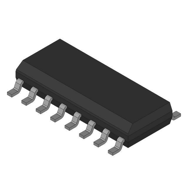
➤ 16-pin narrow SOIC
Pin Connections
Battery self-discharge is estimated
based on an internal timer and temperature sensor. Compensations for
battery temperature and rate of
charge or discharge are applied to
the charge, discharge, and
selfdischarge calculations to provide
available charge information across
a wide range of operating conditions.
Initial battery capacity is set using
the PROG1-4 and SPFC pins. Actual
battery capacity is automatically
“learned” in the course of a discharge cycle from full to empty and
may be displayed depending on the
display mode.
Nominal available charge may be directly indicated using a five-segment LED display. These segments
are used to graphically indicate
nominal available charge.
The bq2011K supports a simple
single-line bidirectional serial link to
an external processor (common
ground). The bq2011K outputs battery information in response to external commands over the serial link. To
support subassembly testing, the
outputs may also be controlled by
command. The external processor
may also overwrite some of the
bq2011K gas gauge data registers.
The bq2011K may operate directly
from four cells. With the REF output and an external transistor, a
simple, inexpensive regulator can be
built to provide VCC from a greater
number of cells.
Internal registers include available
charge, temperature, capacity, battery
ID, and battery status.
Pin Names
LCOM
LCOM
1
16
VCC
SEG1/PROG1
2
15
REF
SEG2/PROG2
3
14
NC
SEG3/PROG3
4
13
DQ
SEG4/PROG4
5
12
RBI
SEG5
6
11
SB
SPFC
7
10
DISP
VSS
8
9
SR
16-Pin Narrow SOIC
PN2011JK.eps
LED common output
SEG1/PROG1 LED segment 1/ Program
1 input
SEG2/PROG2 LED segment 2 / Program
2 input
SEG3/PROG3 LED segment 3/ Program
3 input
SEG4/PROG4 LED segment 4/ Program
4 input
SEG5
LED segment 5
SPFC
Programmed full count
selection input
10/97 B
1
REF
Voltage reference output
NC
No connect
DQ
Serial communications
input/output
RBI
Register backup input
SB
Battery sense input
DISP
Display control input
SR
Sense resistor input
VCC
3.0–6.5V
VSS
Negative battery terminal
�bq2011K
Pin Descriptions
LCOM
LED common
No connect
DISP
Display control input
DISP floating allows the LED display to
be active during certain charge and discharge conditions. Transitioning DISP
low activates the display for 4 ± 0.5 seconds.
Open-drain output switches VCC to source current for the LEDs. The switch is off during initialization to allow reading of PROG1-4 pull-up
or pull-down program resistors. LCOM is high
impedance when the display is off.
SEG1–
SEG5
NC
SB
LED display segment outputs
This input monitors the single-cell voltage
potential through a high-impedance resistive divider network for the end-of-discharge
voltage (EDV) threshold and maximum cell
voltage (MCV).
Each output may activate an LED to sink
the current sourced from LCOM, the battery,
or VCC.
PROG1–
PROG4
Programmed full count selection inputs
(dual function with SEG1 - SEG4)
RBI
DQ
Programmed full count selection input
Serial I/O pin
This is an open-drain bidirectional pin.
This three-level input pin along with PROG1-3
define the programmed full count (PFC)
thresholds described in Table 1. The state of
the SPFC pin is only read immediately after
a reset condition.
SR
Register backup input
This input is used to provide backup potential to the bq2011K registers during periods
when VCC < 3V. A storage capacitor should
be connected to RBI.
These three-level input pins define the programmed full count (PFC) in conjunction
with SPFC pin, define the display mode and
enable or disable self-discharge.
SPFC
Secondary battery input
REF
Voltage reference output for regulator
REF provides a voltage reference output for
an optional micro-regulator.
Sense resistor input
VCC
Supply voltage input
The voltage drop (VSR) across the sense resistor RS is monitored and integrated over
time to interpret charge and discharge activity. The SR input is tied to the low side of
the sense resistor and battery pack ground
(see Figure 1). VSR > VSS indicates discharge,
and VSR < VSS indicates charge. The effective voltage drop, VSRO, as seen by the
bq2011K is VSR + VOS (see Table 4).
VSS
Ground
2
�bq2011K
Figure 1 shows a typical battery pack application of the
bq2011K using the LED display with absolute mode as a
charge-state indicator. The absolute display mode uses
the programmed full count (PFC) as the full reference,
forcing each segment of the display to represent a fixed
amount of charge. A push-button display feature is
available for momentarily enabling the LED display.
Functional Description
General Operation
The bq2011K determines battery capacity by monitoring
the amount of charge input to or removed from a rechargeable battery. The bq2011K measures discharge and charge
currents, estimates self-discharge, monitors the battery for
low-battery voltage thresholds, and compensates for temperature and charge/discharge rates. The charge measurement is made by monitoring the voltage across a smallvalue series sense resistor between the battery’s negative
terminal and ground. The available battery charge is determined by monitoring this voltage over time and correcting the measurement for the environmental and operating
conditions.
The bq2011K monitors the charge and discharge currents as a voltage across a sense resistor (see RS in Figure 1). A filter between the negative battery terminal
and the SR pin may be required if the rate of change of
the battery current is too great.
Register Backup
The bq2011K RBI input pin is intended to be used with
a storage capacitor to provide backup potential to the in-
R1
bq2011K
Gas Gauge IC
Q1
ZVNL110A
REF
LCOM
SEG1/PROG1
C1
0.1 F
VCC
RB1
VCC
SB
SEG2/PROG2
RB2
SEG3/PROG3
DISP
SEG4/PROG4
VSS
SEG5
RS
SR
SPFC
RBI
DQ
Charger
Indicates optional.
Directly connect to VCC across 4 cells (4.8V nominal and should not
exceed 6.5V) with a resistor and a Zener diode to limit voltage during charge.
Otherwise, R1, C1, and Q1 are needed for regulation of >4 cells.
Load
Programming resistors and ESD-protection diodes are not shown.
R-C on SR may be required (application-specific), where the maximum R should not exceed 20K.
FG201103.eps
Figure 1. Application Diagram: LED Display, Absolute Mode
3
�bq2011K
ternal bq2011K registers when VCC momentarily drops below 3.0V. VCC is output on RBI when VCC is above 3.0V.
TMPGG (hex)
After VCC rises above 3.0V, the bq2011K checks the internal
registers for data loss or corruption. If data has changed,
then the NAC register is cleared, and the LMD register is
loaded with the initial PFC.
Voltage Thresholds
In conjunction with monitoring VSR for charge/discharge
currents, the bq2011K monitors the single-cell battery potential through the SB pin. The single-cell voltage potential is determined through a resistor-divider network per
the following equation:
RB1
= N −1
RB2
where N is the number of cells, RB1 is connected to the
positive battery terminal, and RB2 is connected to the
negative battery terminal. The single-cell battery voltage is monitored for the end-of-discharge voltage (EDV)
and for maximum cell voltage (MCV). The EDV threshold level is used to determine when the battery has
reached an “empty” state, and the MCV threshold is used
for fault detection during charging. The MCV threshold
for the bq2011K is fixed at:
0x
< -30°C
1x
-30°C to -20°C
2x
-20°C to -10°C
3x
-10°C to 0°C
4x
0°C to 10°C
5x
10°C to 20°C
6x
20°C to 30°C
7x
30°C to 40°C
8x
40°C to 50°C
9x
50°C to 60°C
Ax
60°C to 70°C
Bx
70°C to 80°C
Cx
> 80°C
Layout Considerations
The bq2011K measures the voltage differential between
the SR and VSS pins. VOS (the offset voltage at the SR
pin) is greatly affected by PC board layout. For optimal
results, the PC board layout should follow the strict rule of
a single-point ground return. Sharing high-current
ground with small signal ground causes undesirable noise
on the small signal nodes. Additionally:
VMCV = 2.00V
The EDV threshold varies as a function of discharge current as follows:
VSRO (mV)
0 < VSRO ≤ 10
10 < VSRO ≤ 20
20 < VSRO ≤ 40
40 < VSRO ≤ 60
VSRO > 60
Temperature Range
VEDV (V)
1.160
1.124
1.060
0.960
0 (OVLD)
Reset
Reset can be accomplished with a command over the serial port as described on page 13.
■
The capacitors (SB and VCC) should be placed as
close as possible to the SB and VCC pins, respectively,
and their paths to VSS should be as short as possible.
A high-quality ceramic capacitor of 0.1µf is
recommended for VCC.
■
The sense resistor (RS) should be as close as possible
to the bq2011K.
■
The R-C on the SR pin should be located as close as
possible to the SR pin. The maximum R should not
exceed 20K.
Gas Gauge Operation
The operational overview diagram in Figure 2 illustrates the operation of the bq2011K. The bq2011K accumulates a measure of charge and discharge currents, as
well as an estimation of self-discharge. Charge currents
are temperature and rate compensated, whereas selfdischarge is only temperature compensated.
Temperature
The bq2011K internally determines the temperature in
10°C steps centered from -35°C to +85°C. The temperature steps are used to adapt charge and discharge rate
compensations, self-discharge counting, and available
charge display translation. The temperature range is
available over the serial port in 10°C increments as
shown below:
The main counter, Nominal Available Charge (NAC),
represents the available battery capacity at any given
time. Battery charging increments the NAC register,
while battery discharging and self-discharge decrement
4
�bq2011K
the NAC register and increment the DCR (Discharge
Count Register).
2.
Programmed Full Count (PFC) or initial battery capacity:
The Discharge Count Register (DCR) is used to update
the Last Measured Discharge (LMD) register only if a
complete battery discharge from full to empty occurs
without any partial battery charges. Therefore, the
bq2011K adapts its capacity determination based on the
actual conditions of discharge.
The initial LMD and gas gauge rate values are programmed by using PFC. The PFC also provides the
100% reference for the absolute display mode. The
bq2011K is configured for a given application by selecting a PFC value from Table 1. The correct PFC
may be determined by multiplying the rated battery capacity in mAh by the sense resistor value:
The battery’s initial capacity is equal to the Programmed Full Count (PFC) shown in Table 1. Until
LMD is updated, NAC counts up to but not beyond this
threshold during subsequent charges. This approach allows the gas gauge to be charger-independent and compatible with any type of charge regime.
1.
Battery capacity (mAh) * sense resistor (Ω) =
PFC (mVh)
Selecting a PFC slightly less than the rated capacity for absolute mode provides capacity above the
full reference for much of the battery’s life.
Last Measured Discharge (LMD) or learned
battery capacity:
Example: Selecting a PFC Value
LMD is the last measured discharge capacity of the
battery. On initialization (application of VCC or battery replacement), LMD = PFC. During subsequent
discharges, the LMD is updated with the latest
measured capacity in the Discharge Count Register
(DCR) representing a discharge from full to below
EDV. A qualified discharge is necessary for a capacity transfer from the DCR to the LMD register.
The LMD also serves as the 100% reference threshold used by the relative display mode.
Inputs
Given:
Sense resistor = 0.002Ω
Number of cells = 6
Capacity = 1800mAh, NiCd cells
Current range = 1A to 80A
Absolute display mode
Self-discharge = C 80
Voltage drop across sense resistor = 2mV to 160mV
Charge
Current
Discharge
Current
Self-Discharge
Timer
Rate and
Temperature
Compensation
Temperature
Compensation
+
Main Counters
and Capacity
Reference (LMD)
+
-
Nominal
Available
Charge
(NAC)
<
Last
Measured
Discharged
(LMD)
Temperature Step,
Other Data
Temperature
Translation
Outputs
Chip-Controlled
Available Charge
LED Display
+
Discharge
Count
Qualified Register
(DCR)
Transfer
Serial
Port
FG201104.eps
Figure 2. Operational Overview
5
�bq2011K
Therefore:
3.
1800mAh * 0.002Ω = 3.6mVh
Nominal Available Charge (NAC):
NAC counts up during charge to a maximum value
of LMD and down during discharge and self discharge to 0. NAC is reset to 0 on initialization and
on the first valid charge following discharge to EDV.
To prevent overstatement of charge during periods
of overcharge, NAC stops incrementing when NAC
= LMD.
Select:
PFC = 35840 counts or 3.39mVh
SPFC = Z (float)
PROG1, PROG2 = H or Z
PROG3 = L
PROG4 = H or Z
Note: NAC is set to the value in LMD when
PROG4 is pulled low during a reset.
The initial full battery capacity is 3.39mVh (1695mAh) until the bq2011K “learns” a new capacity with a qualified
discharge from full to EDV.
Table 1. bq2011K Programmed Full Count mVh Selections
Programmed
Full Count (PFC)
mVh
Scale
40192
3.81
1
32256
3.05
1
28928
2.74
1
Display
Mode
SPFC
PROG1
PROG2
PROG3
10560
H
H or Z
H or Z
H or Z
10560
Z
H or Z
H or Z
H or Z
L
H or Z
H or Z
H or Z
10560
H
L
H or Z
H or Z
10560
Z
L
H or Z
H or Z
10560
L
L
H or Z
H or Z
10560
Absolute
25856
2.45
1
35840
3.39
1
23296
2.21
1
Table 2. Programmed Self-Discharge
PROG4
NAC Reset Value
Self-Discharge
H or Z
NAC = 0
Enabled
L
NAC = PFC
Disabled
6
�bq2011K
4.
Discharge Count Register (DCR):
Self-Discharge Estimation
The DCR counts up during discharge independent
of NAC and could continue increasing after NAC
has decremented to 0. Prior to NAC = 0 (empty
battery), both discharge and self-discharge increment the DCR. After NAC = 0, only discharge increments the DCR. The DCR resets to 0 when NAC
= LMD. The DCR does not roll over but stops
counting when it reaches FFFFh.
The bq2011K continuously decrements NAC and increments DCR for self-discharge based on time and temperature. The self-discharge count rate is programmed
to be a nominal 1 80 * NAC rate per day or disabled per
Table 2. This is the rate for a battery temperature between 20–30°C. The NAC register cannot not be decremented below 0.
The DCR value becomes the new LMD value on the
first charge after a valid discharge to VEDV if:
Count Compensations
The bq2011K determines fast charge when the NAC updates at a rate of ≥2 counts/sec. Charge activity is compensated for temperature and rate before updating the
NAC and/or DCR. Self-discharge estimation is compensated for temperature before updating the NAC or DCR.
No valid charge initiations (charges greater than
256 NAC counts; or 0.006 – 0.01C) occurred during
the period between NAC = LMD and EDV detected.
The self-discharge count is not more than 4096
counts (8% to 18% of PFC, specific percentage
threshold determined by PFC).
Charge Compensation
Two charge efficiency factors are used for trickle charge
and fast charge. Fast charge is defined as a rate of
charge resulting in ≥ 2 NAC counts/sec (≥ 0.15C to 0.32C
depending on PFC selections; see Table 1). The compensation defaults to the fast charge factor until the actual
charge rate is determined.
The temperature is ≥ 0°C when the EDV level is
reached during discharge.
The valid discharge flag (VDQ) indicates whether
the present discharge is valid for LMD update.
Charge Counting
Temperature adapts the charge rate compensation factors over three ranges between nominal, warm, and hot
temperatures. The compensation factors are shown below.
Charge activity is detected based on a negative voltage
on the VSR input. If charge activity is detected, the
bq2011K increments NAC at a rate proportional to VSRO
(VSR + VOS) and, if enabled, activates an LED display
if VSRO < -2mV. Charge actions increment the NAC after compensation for charge rate and temperature.
The bq2011K determines a valid charge activity sustained at a continuous rate equivalent to VSRO < -400µV.
A valid charge equates to a sustained charge activity
greater than 256 NAC counts. Once a valid charge is detected, charge counting continues until V SRO rises
above -400µV.
Charge
Temperature
Trickle Charge
Compensation
Fast Charge
Compensation
50°C
0.70
0.85
Discharge Counting
Discharge Compensation
All discharge counts where VSRO > 500µV cause the
NAC register to decrement and the DCR to increment.
Exceeding the fast discharge threshold (FDQ) if the rate
is equivalent to VSRO > 2mV activates the display, if enabled. The display remains active for 10 seconds after
VSRO falls below 2mV.
Corrections for the rate of discharge are made by adjusting EDV thresholds. The compensation factor used during discharge is set to 1.00 for all rates and temperatures. The recoverable charge at colder temperatures is
adjusted for display purposes only. See page 13.
7
�bq2011K
Self-Discharge Compensation
Current-Sensing Error
The self-discharge compensation is programmed for a
nominal rate of 1 80 * NAC per day or disabled. This is
the rate for a battery within the 20–30°C temperature
range (TMPGG = 6x). This rate varies across 8 ranges
from 70°C, doubling with each higher temperature step (10°C). See Table 3.
Table 4 illustrates the current-sensing error as a function of V SR . A digital filter eliminates charge and
discharge counts to the NAC register when VSRO (VSR +
VOS) is between -400µV and 500µV.
Table 3. Self-Discharge Compensation
The bq2011K includes a simple single-pin (DQ plus return) serial data interface. A host processor uses the interface to access various bq2011K registers. Battery characteristics may be easily monitored by adding a single contact to the battery pack. The open-drain DQ pin on the
bq2011K should be pulled up by the host system, or may be
left floating if the serial interface is not used.
Temperature
Range
Communicating With the bq2011K
Self-Discharge Compensation
Typical Rate/Day
< 10°C
NAC
10–20°C
NAC
20–30°C
NAC
30–40°C
NAC
40–50°C
NAC
50–60°C
NAC
60–70°C
NAC
> 70°C
NAC
320
160
The interface uses a command-based protocol, where the
host processor sends a command byte to the bq2011K.
The command directs the bq2011K to either store the
next eight bits of data received to a register specified by
the command byte or output the eight bits of data specified by the command byte.
80
40
20
10
The communication protocol is asynchronous return-toone. Command and data bytes consist of a stream of eight
bits that have a maximum transmission rate of 333
bits/sec. The least-significant bit of a command or data
byte is transmitted first. The protocol is simple enough
that it can be implemented by most host processors using
either polled or interrupt processing. Data input from the
bq2011K may be sampled using the pulse-width capture
timers available on some microcontrollers.
5
2 .5
Error Summary
The LMD is susceptible to error on initialization or if no
updates occur. On initialization, the LMD value includes the error between the programmed full capacity
and the actual capacity. This error is present until a
valid discharge occurs and LMD is updated (see the
DCR description in the “Layout Considerations” section).
The other cause of LMD error is battery wear-out. As
the battery ages, the measured capacity must be adjusted to account for changes in actual battery capacity.
Communication is normally initiated by the host processor sending a BREAK command to the bq2011K. A
BREAK is detected when the DQ pin is driven to a
logic-low state for a time, tB or greater. The DQ pin
should then be returned to its normal ready-high logic
state for a time, tBR. The bq2011K is now ready to receive a command from the host processor.
The return-to-one data bit frame consists of three distinct
sections. The first section is used to start the transmission
by either the host or the bq2011K taking the DQ pin to a
Table 4. bq2011K Current-Sensing Errors
Symbol
Parameter
Typical
INL
Integrated non-linearity
error
±2
INR
Integrated nonrepeatability error
±1
Maximum
Units
Notes
±4
%
Add 0.1% per °C above or below 25°C
and 1% per volt above or below 4.25V.
±2
%
Measurement repeatability given
similar operating conditions.
8
�bq2011K
logic-low state for a period, tSTRH,B. The next section is the
actual data transmission, where the data should be valid by
a period, tDSU, after the negative edge used to start communication. The data should be held for a period, tDV, to allow
the host or bq2011K to sample the data bit.
The W/R bit of the command register is used to select
whether the received command is for a read or a write
function.
The final section is used to stop the transmission by returning the DQ pin to a logic-high state by at least a period,
tSSU, after the negative edge used to start communication.
The final logic-high state should be held until a period, tSV,
to allow time to ensure that the bit transmission was
stopped properly. The timings for data and break communication are given in the serial communication timing specification and illustration sections.
CMDR Bits
The W/R values are:
7
6
5
4
3
2
1
0
W/R
-
-
-
-
-
-
-
Where W/R is:
Communication with the bq2011K is always performed
with the least-significant bit being transmitted first.
Figure 3 shows an example of a communication sequence to read the bq2011K NAC register.
bq2011K Registers
0
The bq2011K outputs the requested register contents specified by the address portion of CMDR.
1
The following eight bits should be written
to the register specified by the address portion of CMDR.
The lower seven-bit field of CMDR contains the address
portion of the register to be accessed. Attempts to write
to invalid addresses are ignored.
The bq2011K command and status registers are listed in
Table 5 and described below.
Command Register (CMDR)
CMDR Bits
The write-only CMDR register is accessed when eight
valid command bits have been received by the bq2011K.
The CMDR register contains two fields:
■
W/R bit
■
Command address
7
-
6
5
AD6 AD5
4
AD4
3
AD3
2
AD2
1
0
AD1
AD0
(LSB)
Primary Status Flags Register (FLGS1)
The read-only FLGS1 register (address=01h) contains
the primary bq2011K flags.
Written by Host to bq2011K
CMDR = 03h
LSB
MSB
Break 1 1 0 0 0 0 0 0
Received by Host to bq2011K
NAC = 65h
LSB
MSB
1 0 1 0 0 11 0
DQ
TD201103.eps
Figure 3. Typical Communication With the bq2011K
9
�bq2011K
Table 5. bq2011K Command and Status Registers
Symbol
Register
Name
Control Field
Loc.
(hex)
Read/
Write
7(MSB)
6
5
4
3
2
1
0(LSB)
CMDR
Command
register
00h
Write
W/R
AD6
AD5
AD4
AD3
AD2
AD1
AD0
FLGS1
Primary
status flags
register
01h
Read
CHGS
BRP
MCV
n/u
VDQ
n/u
EDV
n/u
Temperature
TMPGG and gas gauge 02h
register
Read
TMP3
TMP2
TMP1
TMP0
GG3
GG2
GG1
GG0
NACH
Nominal
available
charge high
byte register
03h
R/W
NACH7 NACH6 NACH5 NACH4 NACH3 NACH2 NACH1 NACH0
NACL
Nominal
available
charge low
byte register
17h
Read
NACL7 NACL6
BATID
Battery
identification
register
04h
R/W
BATID7 BATID6 BATID5 BATID4 BATID3 BATID2 BATID1 BATID0
LMD
Last measured discharge register
05h
R/W
LMD7
LMD6
LMD5
LMD4
LMD3
LMD2
LMD1
LMD0
FLGS2
Secondary
status flags
register
06h
Read
CR
DR2
DR1
DR0
n/u
n/u
n/u
OVLD
OCTL
Output control register
0ah
Write
1
OC5
OC4
OC3
OC2
OC1
n/u
OCE
RST
Reset register
39h
Write
RST
0
0
0
0
0
0
0
Note:
n/u = not used
10
NACL5
NACL4 NACL3 NACL2 NACL1 NACL0
�bq2011K
mains set until either LMD is updated or one of three
actions that can clear VDQ occurs:
The charge status flag (CHGS) is asserted when a
valid charge rate is detected. Charge rate is deemed
valid when VSRO < -400µV. A VSRO of greater than400µV or discharge activity clears CHGS.
■
The self-discharge count register (SDCR) has
exceeded the maximum acceptable value (4096
counts) for an LMD update.
■
A valid charge action equal to 256 NAC counts with
VSRO < -400µV.
■
The EDV flag was set at a temperature below 0°C
The CHGS values are:
FLGS1 Bits
7
6
5
4
3
2
1
0
CHGS
-
-
-
-
-
-
-
The VDQ values are:
Where CHGS is:
0
1
FLGS1 Bits
Either discharge activity detected or VSRO >
-400µV
VSRO < -400µV
The battery replaced flag (BRP) is asserted whenever
the potential on the SB pin (relative to VSS), VSB, rises
above 0.1V and determines the internal registers have
been corrupted. The BRP flag is also set when the
bq2011K is reset (see the RST register description).
BRP is cleared if either the bq2011K is charged until
NAC = LMD or discharged until EDV is reached. BRP =
1 signifies that the device has been reset.
5
4
3
2
1
0
-
BRP
-
-
-
-
-
-
bq2011K is charged until NAC = LMD or
discharged until the EDV flag is asserted
1
Initial or full VCC reset, or a serial port initiated reset has occurred
6
5
4
3
2
1
0
-
-
MCV
-
-
-
-
-
0
VDQ
-
-
-
0
SDCR ≥ 4096, subsequent valid charge action detected, or EDV is asserted with the
temperature less than 0°C
1
On first discharge after NAC = LMD
7
6
5
4
3
2
1
0
-
-
-
-
-
-
EDV
-
0
Valid charge action detected
1
VSB < VEDV
The read-only TMPGG register (address=02h) contains
two data fields. The first field contains the battery temperature. The second field contains the available charge
from the battery.
TMPGG Temperature Bits
7
Where MCV is:
VSB > 2.0V
1
-
Temperature and Gas Gauge Register (TMPGG)
FLGS1 Bits
7
1
2
-
Where EDV is:
The MCV values are:
VSB < 2.0V
3
-
FLGS1 Bits
The maximum cell voltage flag (MCV) is asserted
whenever the potential on the SB pin (relative to VSS) is
above 2.0V. The MCV flag is asserted until the condition
causing MCV is removed.
0
4
-
The EDV values are:
Where BRP is:
0
5
The end-of-discharge warning flag (EDV) warns the
user that the battery is empty. SEG1 blinks at a 4Hz
rate. EDV detection is disabled if OVLD = 1. The EDV
flag is latched until a valid charge has been detected.
FLGS1 Bits
6
6
Where VDQ is:
The BRP values are:
7
7
6
TMP3 TMP2
5
4
TMP1 TMP0
3
2
1
-
-
-
0
The bq2011K contains an internal temperature sensor.
The temperature is used to set charge efficiency factors
as well as to adjust the self-discharge coefficient. The
temperature register contents may be translated as
shown in Table 6.
The valid discharge flag (VDQ) is asserted when the
bq2011K is discharged from NAC=LMD. The flag re-
11
�bq2011K
The adjustment between > 0°C and -20°C < T < 0°C has
a 4°C hysteresis.
Table 6. Temperature Register Contents
Nominal Available Charge Register (NAC)
TMP3
TMP2
TMP1
TMP0
Temperature
0
0
0
0
T < -30°C
0
0
0
1
-30°C < T < -20°C
0
0
1
0
-20°C < T < -10°C
0
0
1
1
-10°C < T < 0°C
0
1
0
0
0°C < T < 10°C
0
1
0
1
10°C < T < 20°C
0
1
1
0
20°C < T < 30°C
0
1
1
1
30°C < T < 40°C
If SEG4 = 0 on reset, then NACH = PFC and NACL = 0.
If SEG4 = Z or H, the NACH and NACL registers are
cleared to zero. NACL stops counting when NACH
reaches zero. When the bq2011K detects a valid charge,
NACL resets to zero; writing to the NAC register affects
the available charge counts and, therefore, affects the
bq2011K gas gauge operation.
1
0
0
0
40°C < T < 50°C
Battery Identification Register (BATID)
1
0
0
1
50°C < T < 60°C
1
0
1
0
60°C < T < 70°C
1
0
1
1
70°C < T < 80°C
1
1
0
0
T > 80°C
The read/write NACH register (address=03h) and the
read-only NACL register (address=17h) are the main
gas gauging registers for the bq2011K. The NAC registers are incremented during charge actions and decremented during discharge and self-discharge actions.
The correction factors for charge/discharge efficiency are
applied automatically to NAC.
The read/write BATID register (address=04h) is available for use by the system to determine the type of battery pack. The BATID contents are retained as long as
VCC is greater than 2V. The contents of BATID have no
effect on the operation of the bq2011K. There is no default setting for this register.
Last Measured Discharge Register (LMD)
LMD is a read/write register (address=05h) that the
bq2011K uses as a measured full reference. The
bq2011K adjusts LMD based on the measured discharge
capacity of the battery from full to empty. In this way
the bq2011K updates the capacity of the battery. LMD
is set to PFC during a bq2011K reset.
The bq2011K calculates the available charge as a function of NAC, temperature, and a full reference, either
LMD or PFC. The results of the calculation are available via the display port or the gas gauge field of the
TMPGG register. The register is used to give available
capacity in 1 16 increments from 0 to 15 16.
Secondary Status Flags Register (FLGS2)
TMPGG Gas Gauge Bits
7
6
5
4
3
2
1
0
-
-
-
-
GG3
GG2
GG1
GG0
The read-only FLGS2 register (address=06h) contains
the secondary bq2011K flags.
The charge rate flag (CR) is used to denote the fast
charge regime. Fast charge is assumed whenever a
charge action is initiated. The CR flag remains asserted
if the charge rate does not fall below 2 counts/sec.
The gas gauge display and the gas gauge portion of the
TMPGG register are adjusted for cold temperature dependencies. A piece-wise correction is performed as follows:
Temperature
The CR values are:
FLGS2 Bits
Available Capacity Calculation
> 0°C
NAC / “Full Reference”
-20°C < T < 0°C
0.75 * NAC / “Full Reference”
< -20°C
0.5 * NAC / “Full Reference”
7
6
5
4
3
2
1
0
CR
-
-
-
-
-
-
-
Where CR is:
12
0
When charge rate falls below 2 counts/sec
1
When charge rate is above 2 counts/sec
�bq2011K
The fast charge regime efficiency factors are used when
CR = 1. When CR = 0, the trickle charge efficiency factors are used. The time to change CR varies due to the
user-selectable count rates.
Reset Register (RST)
The reset register (address=39h) provides the means to
perform a software-controlled reset of the device. A full
device reset may be accomplished by first writing LMD
(address = 05h) to 00h and then writing the RST register contents from 00h to 80h. Setting any bit other than
the most-significant bit of the RST register is not allowed, and results in improper operation of the
bq2011K.
The discharge rate flags, DR2–0, are bits 6–4.
FLGS2 Bits
7
6
5
4
3
2
1
-
DR2
DR1
DR0
-
-
-
0
Resetting the bq2011K sets the following:
They are used to determine the present discharge regime as follows:
■
LMD = PFC
■
VDQ, OCE, and NAC = 0
(NAC = PFC when PROG4 = L)
BRP = 1
DR2
DR1
DR0
VSRO(mV)
0
0
0
0 < VSRO ≤ 10
■
0
0
1
10 < VSRO ≤ 20
Display
0
1
0
20 < VSRO ≤ 40
0
1
1
40 < VSRO ≤ 60
1
0
0
VSRO > 60
The bq2011K can directly display capacity information
using low-power LEDs. If LEDs are used, the segment
pins should be tied to VCC, the battery, or the LCOM pin
through resistors for programming the bq2011K.
The bq2011K displays the battery charge state in absolute mode. In absolute mode, each segment represents a
fixed amount of charge, based on the initial PFC. In absolute mode, each segment represents 20% of the PFC.
As the battery wears out over time, it is possible for the
LMD to be below the initial PFC. In this case, all of the
LEDs may not turn on, representing the reduction in
the actual battery capacity.
The overload flag (OVLD) is asserted when a discharge
overload is detected, VSRO > 60mV. OVLD remains asserted as long as the condition is valid.
FLGS2 Bits
7
6
5
4
3
2
1
0
-
-
-
-
-
-
-
OVLD
The capacity display is also adjusted for the present battery temperature. The temperature adjustment reflects
the available capacity at a given temperature but does not
affect the NAC register. The temperature adjustments are
detailed in the TMPGG register description.
Output Control Register (OCTL)
The write-only OCTL register (address=0ah) provides the
system with a means to check the display connections for
the bq2011K. The segment drivers may be overwritten by
data from OCTL when the least-significant bit of OCTL,
OCE, is set. The data in bits OC5–1 of the OCTL register
(see Table 5 for details) is output onto the segment pins,
SEG5–1, respectively if OCE=1. Whenever OCE is written
to 1, the MSB of OCTL should be set to a 1. The OCE register location must be cleared to return the bq2011K to
normal operation. OCE may be cleared by either writing
the bit to a logic zero via the serial port or by resetting the
bq2011K as explained below. Note: Whenever the OCTL
register is written, the MSB of OCTL should be written to a
logic one.
When DISP is tied to VCC, the SEG1–5 outputs are inactive. When DISP is left floating, the display becomes active during charge if the NAC registers are counting at a
rate equivalent to VSRO < -2mV or fast discharge if the
NAC registers are counting at a rate equivalent to VSRO
> 2mV. When DISP is left floating, the display also becomes active after the detection of a discharge signal
with a minimum amplitude of VSR > 20mV (10A for RS =
0.002Ω) and a minimum pulse width of 25ms. When
DISP is pulled low, the segment outputs become active
for 4s, ± 0.5s.
13
�bq2011K
The segment outputs are modulated as two banks, with
segments 1, 3, and 5 alternating with segments 2 and 4.
The segment outputs are modulated at approximately
320Hz, with each bank active for 30% of the period.
Microregulator
The bq2011K can operate directly from 4 cells. To facilitate the power supply requirements of the bq2011K, an
REF output is provided to regulate an external lowthreshold n-FET. A micropower source for the bq2011K
can be inexpensively built using the FET and an external resistor.
SEG1 blinks at a 4Hz rate whenever VSB has been detected to be below VEDV to indicate a low-battery condition or NAC is less than 10% of PFC.
14
�bq2011K
Absolute Maximum Ratings
Symbol
Parameter
Minimum
Maximum
Unit
VCC
Relative to VSS
-0.3
7.0
V
All other pins
Relative to VSS
-0.3
7.0
V
VSR
Relative to VSS
TOPR
Operating temperature
Note:
Notes
-0.3
7.0
V
Minimum 100Ω series resistor
should be used to protect SR in case
of a shorted battery (see the
bq2011K application note for
details).
0
70
°C
Commercial
Permanent device damage may occur if Absolute Maximum Ratings are exceeded. Functional operation should be limited to the Recommended DC Operating Conditions detailed in this data sheet. Exposure to conditions beyond the operational limits for extended periods of time may affect device reliability.
DC Voltage Thresholds (TA = TOPR; V = 3.0 to 6.5V)
Symbol
Parameter
Minimum
Typical
Maximum
Unit
Notes
0.96 ∗ VEDV
VEDV
1.04 ∗ VEDV
V
SB
-
-
-400
µV
VSR + VOS
VEDV
End-of-discharge warning
VSRQ
Valid charge
VSRD
Valid discharge
500
-
-
µV
VSR + VOS
VMCV
Maximum single-cell voltage
1.95
2.0
2.05
V
SB
Note:
For proper operation of the threshold detection circuit, VCC must be at least 1.5V greater than the voltage being measured.
15
�bq2011K
DC Electrical Characteristics (TA = TOPR)
Symbol
VCC
VOS
VREF
RREF
ICC
Parameter
Supply voltage
Minimum
Typical
Maximum
Unit
Notes
VCC excursion from < 2.0V to ≥
3.0V initializes the unit.
3.0
4.25
6.5
V
-
±50
±150
µV
DISP = VCC
Reference at 25°C
5.7
6.0
6.3
V
IREF = 5µA
Reference at -40°C to +85°C
4.5
-
7.5
V
IREF = 5µA
Reference input impedance
2.0
5.0
-
MΩ
VREF = 3V
-
90
135
µA
VCC = 3.0V, DQ = 0
-
120
180
µA
VCC = 4.25V, DQ = 0
-
170
250
µA
VCC = 6.5V, DQ = 0
Offset referred to VSR
Normal operation
VSB
Battery input
0
-
VCC
V
RSBmax
SB input impedance
10
-
-
MΩ
0 < VSB < VCC
IDISP
DISP input leakage
-
-
5
µA
VDISP = VSS
ILCOM
LCOM input leakage
-0.2
-
0.2
µA
DISP = VCC
IRBI
RBI data-retention current
-
-
100
nA
VRBI > VCC < 3V
RDQ
Internal pulldown
500
-
-
KΩ
VSR
Sense resistor input
-0.3
-
2.0
V
RSR
SR input impedance
VIHPFC
PROG/SPFC logic input high
VILPFC
PROG/SPFC logic input low
VIZPFC
PROG/SPFC logic input Z
IIHPFC
10
-
-
MΩ
VCC - 0.2
-
-
V
VSR > VSS = discharge;
VSR < VSS = charge
-200mV < VSR < VCC
SPFC, PROG1-4
-
-
VSS + 0.2
V
SPFC, PROG1-4
float
-
float
V
SPFC, PROG1-4
PROG/SPFC input high current
-
1.2
-
µA
VPFC = VCC/2
IILPFC
PROG/SPFC input low current
-
1.2
-
µA
VPFC = VCC/2
VOLSL
SEGX output low, low VCC
-
0.1
-
V
VCC = 3V, IOLS ≤ 1.75mA
SEG1–SEG5
VOLSH
SEGX output low, high VCC
-
0.4
-
V
VCC = 6.5V, IOLS ≤ 11.0mA
SEG1–SEG5
VOHML
LCOM output high, low VCC
VCC - 0.3
-
-
V
VCC = 3V, IOHLCOM = -5.25mA
VOHMH
LCOM output high, high VCC
VCC - 0.6
-
-
V
-33
-
-
mA
IOHLCOM LCOM source current
VCC = 6.5V, IOHLCOM = -33.0mA
At VOHLCOM = VCC - 0.6V
IOLS
SEGX sink current
11.0
-
-
mA
At VOLSH = 0.4V, VCC = 6.5V
IOL
Open-drain sink current
5.0
-
-
mA
At VOL = VSS + 0.3V, DQ
IOL ≤ 5mA, DQ
VOL
Open-drain output low
-
-
0.5
V
VIHDQ
DQ input high
2.5
-
-
V
DQ
VILDQ
DQ input low
-
-
0.8
V
DQ
RFLOAT
Float state external impedance
-
5
-
MΩ
Note:
All voltages relative to VSS.
16
SPFC, PROG1-4
�bq2011K
Serial Communication Timing Specification (TA = TOPR)
Symbol
Parameter
Minimum
Typical
Maximum
Unit
tCYCH
Cycle time, host to bq2011K
3
-
-
ms
tCYCB
Cycle time, bq2011K to host
3
-
6
ms
tSTRH
Start hold, host to bq2011K
5
-
-
ns
tSTRB
Start hold, bq2011K to host
500
-
-
µs
tDSU
Data setup
-
-
750
µs
tDH
Data hold
750
-
-
µs
tDV
Data valid
1.50
-
-
ms
tSSU
Stop setup
-
-
2.25
ms
tSH
Stop hold
700
-
-
µs
tSV
Stop valid
2.95
-
-
ms
tB
Break
3
-
-
ms
tBR
Break recovery
1
-
-
ms
Note:
Notes
See note
The open-drain DQ pin should be pulled to at least VCC by the host system for proper DQ operation.
DQ may be left floating if the serial interface is not used.
Serial Communication Timing Illustration
DQ
(R/W "1")
DQ
(R/W "0")
tSTRH
tSTRB
tDH
tDSU
tDV
tSH
tSSU
DQ
(BREAK)
tSV
tCYCH, tCYCB, tB
tBR
TD201002.eps
17
�bq2011K
16-Pin SOIC Narrow (SN)
16-Pin SN (SOIC Narrow)
D
e
Dimension
Minimum
A
0.060
A1
0.004
B
0.013
C
0.007
D
0.385
E
0.150
e
0.045
H
0.225
L
0.015
All dimensions are in inches.
B
E
H
A
C
A1
.004
L
18
Maximum
0.070
0.010
0.020
0.010
0.400
0.160
0.055
0.245
0.035
�bq2011K
Data Sheet Revision History
Change No. Page No.
Description
Nature of Change
1
6
Removed relative display mode from Table 1 Correction
Notes:
Change 1 = Oct. 1997 B changes from Oct. 1995.
Ordering Information
bq2011K
Temperature Range:
blank = Commercial (0 to +70°C)
Package Option:
SN = 16-pin narrow SOIC
Device:
bq2011K Gas Gauge IC
19
�PACKAGE OPTION ADDENDUM
www.ti.com
11-Oct-2005
PACKAGING INFORMATION
Orderable Device
Status (1)
Package
Type
Package
Drawing
Pins Package Eco Plan (2)
Qty
BQ2011KSN-D121
OBSOLETE
SOIC
D
16
TBD
Call TI
Call TI
BQ2011KSN-D121TR
OBSOLETE
SOIC
D
16
TBD
Call TI
Call TI
Lead/Ball Finish
MSL Peak Temp (3)
(1)
The marketing status values are defined as follows:
ACTIVE: Product device recommended for new designs.
LIFEBUY: TI has announced that the device will be discontinued, and a lifetime-buy period is in effect.
NRND: Not recommended for new designs. Device is in production to support existing customers, but TI does not recommend using this part in
a new design.
PREVIEW: Device has been announced but is not in production. Samples may or may not be available.
OBSOLETE: TI has discontinued the production of the device.
(2)
Eco Plan - The planned eco-friendly classification: Pb-Free (RoHS) or Green (RoHS & no Sb/Br) - please check
http://www.ti.com/productcontent for the latest availability information and additional product content details.
TBD: The Pb-Free/Green conversion plan has not been defined.
Pb-Free (RoHS): TI's terms "Lead-Free" or "Pb-Free" mean semiconductor products that are compatible with the current RoHS requirements
for all 6 substances, including the requirement that lead not exceed 0.1% by weight in homogeneous materials. Where designed to be soldered
at high temperatures, TI Pb-Free products are suitable for use in specified lead-free processes.
Green (RoHS & no Sb/Br): TI defines "Green" to mean Pb-Free (RoHS compatible), and free of Bromine (Br) and Antimony (Sb) based flame
retardants (Br or Sb do not exceed 0.1% by weight in homogeneous material)
(3)
MSL, Peak Temp. -- The Moisture Sensitivity Level rating according to the JEDEC industry standard classifications, and peak solder
temperature.
Important Information and Disclaimer:The information provided on this page represents TI's knowledge and belief as of the date that it is
provided. TI bases its knowledge and belief on information provided by third parties, and makes no representation or warranty as to the
accuracy of such information. Efforts are underway to better integrate information from third parties. TI has taken and continues to take
reasonable steps to provide representative and accurate information but may not have conducted destructive testing or chemical analysis on
incoming materials and chemicals. TI and TI suppliers consider certain information to be proprietary, and thus CAS numbers and other limited
information may not be available for release.
In no event shall TI's liability arising out of such information exceed the total purchase price of the TI part(s) at issue in this document sold by TI
to Customer on an annual basis.
Addendum-Page 1
��IMPORTANT NOTICE
Texas Instruments Incorporated and its subsidiaries (TI) reserve the right to make corrections, modifications, enhancements, improvements,
and other changes to its products and services at any time and to discontinue any product or service without notice. Customers should
obtain the latest relevant information before placing orders and should verify that such information is current and complete. All products are
sold subject to TI’s terms and conditions of sale supplied at the time of order acknowledgment.
TI warrants performance of its hardware products to the specifications applicable at the time of sale in accordance with TI’s standard
warranty. Testing and other quality control techniques are used to the extent TI deems necessary to support this warranty. Except where
mandated by government requirements, testing of all parameters of each product is not necessarily performed.
TI assumes no liability for applications assistance or customer product design. Customers are responsible for their products and
applications using TI components. To minimize the risks associated with customer products and applications, customers should provide
adequate design and operating safeguards.
TI does not warrant or represent that any license, either express or implied, is granted under any TI patent right, copyright, mask work right,
or other TI intellectual property right relating to any combination, machine, or process in which TI products or services are used. Information
published by TI regarding third-party products or services does not constitute a license from TI to use such products or services or a
warranty or endorsement thereof. Use of such information may require a license from a third party under the patents or other intellectual
property of the third party, or a license from TI under the patents or other intellectual property of TI.
Reproduction of TI information in TI data books or data sheets is permissible only if reproduction is without alteration and is accompanied
by all associated warranties, conditions, limitations, and notices. Reproduction of this information with alteration is an unfair and deceptive
business practice. TI is not responsible or liable for such altered documentation. Information of third parties may be subject to additional
restrictions.
Resale of TI products or services with statements different from or beyond the parameters stated by TI for that product or service voids all
express and any implied warranties for the associated TI product or service and is an unfair and deceptive business practice. TI is not
responsible or liable for any such statements.
TI products are not authorized for use in safety-critical applications (such as life support) where a failure of the TI product would reasonably
be expected to cause severe personal injury or death, unless officers of the parties have executed an agreement specifically governing
such use. Buyers represent that they have all necessary expertise in the safety and regulatory ramifications of their applications, and
acknowledge and agree that they are solely responsible for all legal, regulatory and safety-related requirements concerning their products
and any use of TI products in such safety-critical applications, notwithstanding any applications-related information or support that may be
provided by TI. Further, Buyers must fully indemnify TI and its representatives against any damages arising out of the use of TI products in
such safety-critical applications.
TI products are neither designed nor intended for use in military/aerospace applications or environments unless the TI products are
specifically designated by TI as military-grade or "enhanced plastic." Only products designated by TI as military-grade meet military
specifications. Buyers acknowledge and agree that any such use of TI products which TI has not designated as military-grade is solely at
the Buyer's risk, and that they are solely responsible for compliance with all legal and regulatory requirements in connection with such use.
TI products are neither designed nor intended for use in automotive applications or environments unless the specific TI products are
designated by TI as compliant with ISO/TS 16949 requirements. Buyers acknowledge and agree that, if they use any non-designated
products in automotive applications, TI will not be responsible for any failure to meet such requirements.
Following are URLs where you can obtain information on other Texas Instruments products and application solutions:
Products
Applications
Audio
www.ti.com/audio
Communications and Telecom www.ti.com/communications
Amplifiers
amplifier.ti.com
Computers and Peripherals
www.ti.com/computers
Data Converters
dataconverter.ti.com
Consumer Electronics
www.ti.com/consumer-apps
DLP® Products
www.dlp.com
Energy and Lighting
www.ti.com/energy
DSP
dsp.ti.com
Industrial
www.ti.com/industrial
Clocks and Timers
www.ti.com/clocks
Medical
www.ti.com/medical
Interface
interface.ti.com
Security
www.ti.com/security
Logic
logic.ti.com
Space, Avionics and Defense
www.ti.com/space-avionics-defense
Power Mgmt
power.ti.com
Transportation and
Automotive
www.ti.com/automotive
Microcontrollers
microcontroller.ti.com
Video and Imaging
www.ti.com/video
RFID
www.ti-rfid.com
Wireless
www.ti.com/wireless-apps
RF/IF and ZigBee® Solutions
www.ti.com/lprf
TI E2E Community Home Page
e2e.ti.com
Mailing Address: Texas Instruments, Post Office Box 655303, Dallas, Texas 75265
Copyright © 2011, Texas Instruments Incorporated
�


 工商网监
湘ICP备2023018690号
工商网监
湘ICP备2023018690号
