RTT
bq2084-V143
DBT
www.ti.com
SLUS732 – SEPTEMBER 2006
SBS v1.1-COMPLIANT GAS GAUGE FOR
USE WITH THE bq29312
FEATURES
•
•
•
•
•
•
•
•
•
•
•
Provides Accurate Measurement of Available
Charge in Li-Ion and Li-Polymer Batteries
Supports the Smart Battery Specification
(SBS) V1.1
Integrated Time Base Removes Need for
External Crystal with Optional Crystal input
Works With the TI bq29312 Analog Front-End
(AFE) Protection IC to Provide Complete Pack
Electronics for 7.2-V, 10.8-V or 14.4-V Battery
Packs With Few External Components
Based on a Powerful Low-Power RISC CPU
Core With High-Performance Peripherals
Integrated Flash Memory Eliminates the Need
for External Configuration EEPROM
Uses 16-Bit Delta Sigma Converter for
Accurate Voltage and Temperature
Measurements
Measures Charge Flow Using a High
Resolution 16-Bit Integrating Converter
– Better Than 0.65-nVh of Resolution
– Self-Calibrating
– Offset Error Less Than 1-µV
Programmable Cell Modeling for Maximum
Battery Fuel Gauge Accuracy
Drives 3-, 4-, or 5-Segment LED Display for
Remaining Capacity Indication
Available in a 38-Pin TSSOP (DBT) Package
APPLICATIONS
•
•
•
Notebook PCs
Medical and Test Equipment
Portable Instrumentation
DESCRIPTION
The bq2084-V143 SBS-compliant gas gauge IC for
battery pack or in-system installation maintains an
accurate record of available charge in Li-ion or
Li-polymer batteries. The bq2084-V143 monitors
capacity and other critical parameters of the battery
pack and reports the information to the system host
controller over a serial communication bus. It is
designed to work with the bq29312 AFE protection
IC to maximize functionality and safety and minimize
component count and cost in smart battery circuits.
Using information from the bq2084-V143, the host
controller can manage remaining battery power to
extend the system run time as much as possible.
The bq2084-V143 uses an integrating converter with
continuous sampling for the measurement of battery
charge and discharge currents. Optimized for
coulomb counting in portable applications, the
self-calibrating integrating converter has a resolution
better than 0.65-nVh and an offset measurement
error of less than 1-µV (typical). For voltage and
temperature reporting, the bq2084-V143 uses a
16-bit A-to-D converter. With the bq29312, the
onboard ADC also monitors the pack and individual
cell voltages in a battery pack and allows the
bq2084-V143 to generate the control signals
necessary to implement the cell balancing and the
required safety protection for Li-ion and Li-polymer
battery chemistries.
The bq2084-V143 supports the Smart Battery Data
(SBData) commands and charge-control functions. It
communicates data using the System Management
Bus (SMBus) 2-wire protocol. The data available
include
the
battery's
remaining
capacity,
temperature, voltage, current, and remaining
run-time predictions.
The bq2084-V143 provides LED drivers and a
pushbutton input to depict remaining battery capacity
from full to empty in 20%, 25%, or 33% increments
with a 3-, 4-, or 5-segment display.
Please be aware that an important notice concerning availability, standard warranty, and use in critical applications of Texas
Instruments semiconductor products and disclaimers thereto appears at the end of this data sheet.
PRODUCTION DATA information is current as of publication date.
Products conform to specifications per the terms of the Texas
Instruments standard warranty. Production processing does not
necessarily include testing of all parameters.
Copyright © 2006, Texas Instruments Incorporated
�bq2084-V143
www.ti.com
SLUS732 – SEPTEMBER 2006
These devices have limited built-in ESD protection. The leads should be shorted together or the device placed in conductive foam
during storage or handling to prevent electrostatic damage to the MOS gates.
DESCRIPTION (CONTINUED)
The bq2084-V143 contains 1k bytes of internal data flash memory, which store configuration information. The
information includes nominal capacity and voltage, self-discharge rate, rate compensation factors, and other
programmable cell-modeling factors used to accurately adjust remaining capacity for use-conditions based on
time, rate, and temperature. The bq2084-V143 also automatically calibrates or learns the true battery capacity in
the course of a discharge cycle from programmable near full to near empty levels.
The bq29312 analog front-end (AFE) protection IC is used to maximize functionality and safety and minimize
component count and cost in smart battery circuits. The bq29312 AFE protection IC provides power to the
bq2084-V143 from a 2-, 3-, or 4-series Li-ion cell stack, eliminating the need for an external regulator circuit.
ORDERING INFORMATION
PACKAGE (1)
TA
38-PIN TSSOP
–20°C to 85°C
(1)
(2)
(3)
(DBT) (2)
bq2084DBT-V143
36-PIN QFN (RTT) (3)
bq2084RTT-V143
For the most current package and ordering information, see the Package Option Addendum at the end
of this document, or see the TI Web site at www.ti.com.
The bq2084DBT-V141 is available in tape and reel. Add an R suffix to the device type (e.g.,
bq2084DBTR-V141) to order tape and reel version.
The bq2084RTT-V140 is available in tape and reel only. Add an T suffix to the device type (e.g.,
bq2084RTTT-V140) to order mini tape and reel version.
ABSOLUTE MAXIMUM RATINGS
over operating free-air temperature range unless otherwise noted (1)
UNIT
Supply voltage range, VDD relative to VSS
(2)
–0.3 V to 4.1 V
Open-drain I/O pins, V(IOD) relative to VSS (2)
–0.3 V to 6 V
Input voltage range to all other pins, VI relative to VSs (2)
TA
Operating free-air temperature range
–20°C to 85°C
Tstg
Storage temperature range
–65°C to 150°C
(1)
(2)
2
–0.3 V to VDD + 0.3 V
Stresses beyond those listed under absolute maximum ratings may cause permanent damage to the device. These are stress ratings
only, and functional operation of the device at these or any other conditions beyond those indicated under recommended operating
conditions is not implied. Exposure to absolute-maximum-rated conditions for extended periods may affect device reliability.
VSS refers to the common node of V(SSA), V(SSD), and V(SSP).
Submit Documentation Feedback
�bq2084-V143
www.ti.com
SLUS732 – SEPTEMBER 2006
ELECTRICAL CHARACTERISTICS
VDD = 3 V to 3.6 V, TA = –20°C to 85°C unless otherwise noted
PARAMETER
VDD
TEST CONDITIONS
MIN
TYP
MAX
3
3.3
3.6
Supply voltage
VDDA and VDDD
IDD
Operating mode current
No flash programming
or LEDs active
I(SLP)
Low-power storage mode current
Sleep mode
VOL
Output voltage low SMBC, SMBD, SDATA, SCLK, SAFE,
PU
IOL = 0.5 mA
0.4
LED1-LED5
IOL = 10 mA
0.4
VIL
VIH
µA
8
µA
–0.3
0.8
DISP
–0.3
0.8
Input voltage high SMBC, SMBD, SDATA, SCLK, EVENT,
PU, PRES, PFIN
2
6
DISP
2
VDD + 0.3
Input voltage range VIN, TS
V(AI2)
Input voltage range SR1, SR2
Z(AI1)
Input impedance SR1, SR2
–0.25 V to 0.25 V
Z(AI2)
Input impedance VIN, TS
0 V–1 V
V
380
Input voltage low SMBC, SMBD, SDATA, SCLK, EVENT,
PU, PRES, PFIN
V(AI1)
UNIT
VSS – 0.3
1.0
VSS – 0.25
0.25
V
V
V
V
V
2.5
MΩ
8
MΩ
POWER-ON RESET
Negative-going voltage input
2.1
2.3
2.5
V
Vhys
Power-on reset hysteresis
50
125
200
mV
POWER ON RESET BEHAVIOR
vs
FREE-AIR TEMPERATURE
2.50
140
2.45
135
2.40
130
VIT-
2.35
125
2.30
120
2.25
115
Vhys
2.20
110
2.15
105
2.10
-20 -10
V hys - Hysterisis Voltage - mV
V IT - Negative Going Input Threshold Voltage - V
VIT+
100
0
10 20 30 40 50 60 70 80
TA - Free-Air Temperature - °C
INTEGRATING ADC CHARACTERISTICS
VDD = 3 V to 3.6 V, TA = –20°C to 85°C unless otherwise noted
PARAMETER
V(SR)
Input voltage range, V(SR2) and V(SR1)
V(SROS)
Input offset
INL
Integral nonlinearity error
TEST CONDITIONS
VSR = V(SR2)– V(SR1)
MIN
TYP
–0.25
MAX
0.25
1
FAST = 0, –0.1 V to 0.8 x Vref
Submit Documentation Feedback
0.004%
UNIT
V
mV
0.018%
3
�bq2084-V143
www.ti.com
SLUS732 – SEPTEMBER 2006
PLL SWITCHING CHARACTERISTICS
VDD = 3 V to 3.6 V, TA = –20°C to 85°C unless otherwise noted
PARAMETER
t(SP)
(1)
Start-up time
TEST CONDITIONS
MIN
TYP MAX
±0.5% frequency error
(1)
2
5
UNIT
ms
The frequency error is measured from the trimmed frequency of the internal system clock, which is 128 x oscillator frequency, nominally
4.194 MHz.
OSCILLATOR
VDD = 3 V to 3.6 V, TA = –20°C to 85°C (unless otherwise noted) (TYP: VDD = 3.3 V, TA = 25°C)
PARAMETER
f(eio)
Frequency error from 32.768 kHz
f(dio)
Frequency drift (1)
f(sio)
f(sxo)
(1)
(2)
TEST CONDITIONS
ROSC = 100k
XCK1 = 12 pF XTAL
ROSC = 100k, TA = 0°C to 50°C
Start-up time (2)
MIN
TYP
MAX
–2%
0.5%
2%
–0.25%
UNIT
0.25%
–1%
1%
ROSC = 100k
200
µs
XCK1 = 12 pF XTAL
250
ms
The frequency drift is measured from the trimmed frequency at VDD = 3.3 V, TA = 25°C.
The start-up time is defined as the time it takes for the oscillator output frequency to be ±1%
DATA FLASH MEMORY CHARACTERISTICS
VDD = 3 V to 3.6 V, TA = –20°C to 85°C unless otherwise noted
PARAMETER
TEST CONDITIONS
MIN
Data retention
See
(1)
10
Flash programming write-cycles
See
(1)
20k
t(WORDPROG)
Word programming time
See
(1)
I(DDPROG)
Flash-write supply current
See
(1)
tDR
(1)
TYP
MAX
UNIT
Years
Cycles
2
ms
8
12
mA
TYP
MAX
UNIT
10
100
nA
Specified by design. Not production tested.
REGISTER BACKUP
PARAMETER
I(RBI)
RBI data-retention input current
V(RBI)
RBI data-retention voltage
(1)
TEST CONDITIONS
MIN
VRBI > 2 V, VDD < VIT
(1)
1.3
V
Specified by design. Not production tested.
SMBus TIMING SPECIFICATIONS
VDD = 3 V to 3.6 V, TA = -20°C to 85°C unless otherwise noted
PARAMETER
SMBus operating frequency
Slave mode, SMBC 50% duty cycle
f(MAS)
SMBus master clock frequency
Master mode, no clock low slave extend
t(BUF)
Bus free time between start and stop
T(HD:STA)
Hold time after (repeated) start
t(SU:STA)
Repeated start setup time
t(SU:STO)
Stop setup time
t(HD:DAT)
Data hold time
tSU:DAT)
Data setup time
t(TIMEOUT)
Error signal/detect
t(LOW)
Clock low period
(1)
4
TEST CONDITIONS
f(SMB)
MIN
TYP MAX
UNIT
10
100
kHz
51.2
kHz
4.7
µs
4
µs
4.7
µs
4
µs
Receive mode
0
Transmit mode
300
ns
250
See
(1)
25
4.7
The bq2084-V143 times out when any clock low exceeds t(TIMEOUT).
Submit Documentation Feedback
ns
35
ms
µs
�bq2084-V143
www.ti.com
SLUS732 – SEPTEMBER 2006
SMBus TIMING SPECIFICATIONS (continued)
VDD = 3 V to 3.6 V, TA = -20°C to 85°C unless otherwise noted
PARAMETER
TEST CONDITIONS
MIN
TYP MAX
4
UNIT
t(HIGH)
Clock high period
See
(2)
50
µs
tLOW:SEXT)
Cumulative clock low slave extend time
See
(3)
25
ms
tLOW:MEXT
Cumulative clock low master extend time
See
(4)
10
ms
tf
Clock/data fall time
(VILMAX – 0.15 V) to (VIHMIN + 0.15 V)
300
ns
tr
Clock/data rise time
0.9 VDD to (VILMAX– 0.15 V)
1000
ns
(2)
(3)
(4)
t(HIGH) Max. is minimum bus idle time. SMBC = 1 for t > 50 ms causes reset of any transaction involving bq2084-V143 that is in
progress.
t(LOW:SEXT) is the cumulative time a slave device is allowed to extend the clock cycles in one message from initial start to the stop.
t(LOW:MEXT) is the cumulative time a master device is allowed to extend the clock cycles in one message from initial start to the stop.
SMBus TIMING DIAGRAMS
Submit Documentation Feedback
5
�bq2084-V143
www.ti.com
SLUS732 – SEPTEMBER 2006
SYSTEM DIAGRAM
Discharge / Charge /
Pre-Charge FET s
Fuse
Pack +
Pre-Charge Control
Fail-Safe
Protection
Power Management
LDO, TOUT and Power Mode Control
Pres
Temperature Measurement
Cell Imbalance Threshold
AND SBS. Current()> Balance IMAX for a period of Cell Imbalance time then the CIM bit in PF Status is set.
Table 6. Cell Balancing and Cell Imbalance Programming
NAME
DF ADDRESS
DESCRIPTION
Cell Balance Threshold
0xe8-0xe9
Sets the maximum voltage in mV that each cell must achieve to initiate cell balancing.
Programming Cell Balance Threshold to 65,535 disables cell balancing.
Cell Balance Min
0xec
Sets in mV the cell differential that must exist to initiate cell balancing
Cell Balance Window
0xea-0xeb
Sets in mV the amount that the cell balance threshold increases during cell balancing
Cell Balance Interval
0xed
Sets the cell balancing time interval in seconds.
Cell Imbalance Threshold
0xee-0xef
Sets the severe imbalance fault limit for cell imbalance detection
Balance IMAX
0xf2-0xf3
Sets the charge current required to allow a cell imbalance to be detected
Cell Imbalance Time
0x134
Sets the time period during which a cell imbalance must be selected for the bq2084 to enter
PF mode.
Submit Documentation Feedback
19
�bq2084-V143
www.ti.com
SLUS732 – SEPTEMBER 2006
DISPLAY PORT
General
The display port drives a 3-, 4-, or 5-LED bar-graph display. The display is activated by a logic signal on the
DISP input. The bq2084-V143 can display RM in either a relative or absolute mode with each LED representing
a percentage of the full-battery reference. In relative mode, the bq2084-V143 uses FCC as the full-battery
reference; in absolute mode, it uses Design Capacity (DC). The DMODE bit in Pack Configuration DF 0x28
programs the bq2084-V143 for the absolute or relative display mode. The LED bits program the 3-, 4-, or 5-LED
option.
Activation
The display may be activated at any time by a high-to-low transition on the DISP input. This is usually
accomplished with a pullup resistor and a pushbutton switch. Detection of the transition activates the display and
starts a 4-s display timer. Reactivation of the display requires that the DISP input return to a logic-high state and
then transition low again. The second high-to-low transition can be detected only after the display timer expires.
If unused, the DISP input must be pulled up to VCC. If the EDV0 bit is set, the bq2084-V143 disables the LED
display.
Display Modes
In relative mode, each LED output represents 20%, 25%, or 33% of the RelativeStateOfCharge() value. In
absolute mode, each LED output represents 20%, 25% or 33% of the AbsoluteStateOfCharge() value. Table 7
shows the display options for 5 LEDs, for 4 LEDs, Table 8 and Table 9 for 3 LEDs. In either mode, the
bq2084-V143 blinks the LED display if RemainingCapacity() is less than Remaining CapacityAlarm(). The
display is disabled if EDV0 = 1.
Table 7. Display Mode for Five LEDs
CONDITION
RELATIVE OR ABSOLUTE
FIVE-LED DISPLAY OPTION
StateOfCharge()
LED1
LED2
LED3
LED4
LED5
EDV0 = 1
OFF
OFF
OFF
OFF
OFF
charge
detection current (DF 0x113/4)
GG Charge OC (set by DF 0x12a to 0x12c)
CHG off, ZVCHG off, DSG on
Same AFE SCC
GG Discharge OC (set by DF 0x12d to 0x12f) CHG on, ZVCHG off, DSG off
Same AFE SCD
NR=0
FAILURE
FET STATUS
EXIT CONDITIONS
AFE OLV
All FETs off
RRES=high
AFE SCC
All FETs off
PRES=high
AFE SCD
All FETs off
PRES=high
GG Charge OC (set by DF 0x12a to 0x12c)
All FETs off
PRES=high
GG Discharge OC (set by DF 0x12d to 0x12f) All FETs off
PRES=high
22
Submit Documentation Feedback
�bq2084-V143
www.ti.com
SLUS732 – SEPTEMBER 2006
The AFE protection features can also recover automatically after AFE Recovery Time (DF 0x160) if the AFE
Recovery Time is set to a nonzero value. When the protection feature is recovered in this manner, it does not
re-trigger for AFE Hold Off Time (DF 0x161).
AFE Integrity Check
The bq2084-V143 checks the programming of the AFE registers at a period determined by AFE Check Time DF
0xfb. The units of the check period are seconds unless the bq2084-V143 is in sleep mode, in which case the
period is AFE Check Time x Sleep Current Multiplier (DF 0xfd). If the data is not correct, the bq2084-V143
increments an internal counter until it reaches the AFE Fail Limit (DF 0xe4). Setting AFE Check Time to 0
disables this function.
When the internal AFE Fail counter reaches AFE Fail Limit, then the AFE bit in PF Status is set.
AFE Watchdog Fault and Clear
The bq29312 has a feature where the 32-kHz output (CLKOUT, pin 35) of the bq2084-V143 is used to drive its
internal clock. If this clock fails, a fault is declared in the AFE. See the bq29312 data sheet for further details.
The fault is cleared automatically on return of the 32-kHz input via the bq2084-V143 CLKOUT pin.
Permanent Failure Mode (SAFE Output)
The SAFE output of the bq2084-V143 provides an additional level of safety control. The active low safety output
can blow a fuse or control another switch on the basis of temperature, pack-voltage cell-voltage, CHG FET
Failure, severe cell imbalance, or an integrity check of the AFE and Data Flash configuration registers.
The bq2084-V143 can also activate the SAFE output and set the PF Flag based on the PFIN input. If this pin is
low for PFIN Time seconds ±1 s, then the PFIN bit in PF Status is set.
The SAFE output can be driven low in any of the following conditions, and the bq2084-V143 sets the PF Flag
register (DF 0x11e) to 0x66 (011001100). The activation of the SAFE output and the setting of the PF Flag can
be enabled or disabled for different safety option per the PF Config (DF 0x11f) register settings.
The SAFE output and PF Flag register can only be cleared using a series of ManufacturerAccess() commands.
Table 12. SAFE Activation Conditions (1)
CONDITION
ACTIONS
Voltage() > Safety Over Voltage (DF 0x6b and 0x6c),
SOV and PF set
Temperature() > Safety Over Temperature in Charge (DF 0x75 and 0x76)
SOTC and PF set
Temperature() > Safety Over Temperature in Discharge (DF 0x77 and 0x78)
SOTD and PF set
When Miscellaneous Configuration (0x2a) bit 13 AC is set, and the number of AFE failures has reached the AFE Fail
Limit (DF 0xe4)
AFE and PF set
When VCELL(MAX) - VCELL(MIN) > Cell Imbalance Threshold (DF 0xee, 0xef) during charging
CIM and PF set
If charge FET is off, and charge current greater than FET Fail charge current stored in DF 0x125-0x126 for the time
determined by FET Fail time in DF 0x129, or if discharge FET is off and discharge current greater than FET Fail
discharge current stored in DF 0x127-0x128 for the time determined by FET Fail time in DF 0x129.
The PFIN input has detected a low state for PFIN Time in consecutive seconds, as determined by DF 0x120
(1)
FETF and PF set
PFIN, PF set
SAFE output activated and PF Flag set only if enabled by PF Config (DF 0x0x11f)
Permanent Failure Status (PF Status)
PF Status DF 0x11d contains the flags for the cause of the permanent failure mode.
b7
b6
b5
b4
b3
b2
b1
b0
PFF
PFIN
FETF
CIM
AFE
SOTD
SOTC
SOV
Submit Documentation Feedback
23
�bq2084-V143
www.ti.com
SLUS732 – SEPTEMBER 2006
SOV
The SOV bit indicates a safety overvoltage occurred which if enabled by PF Config would cause the SAFE
output to activate.
0
SOV fault not detected (default)
1
SOV fault detected
SOTC
The SOTC bit indicates a safety overtemperature in charge occurred which if enabled by PF Config would
cause the SAFE output to activate.
0
SOTC fault not detected (default)
1
SOTC fault detected
SOTD
The SOTD bit indicates a safety overtemperature in discharge occurred which if enabled by PF Config would
cause the SAFE output to activate.
0
SOTD fault not detected (default)
1
SOTD fault detected
AFE
The AFE bit indicates an AFE integrity fault state occurred which if enabled by PF Config would cause the
SAFE output to activate.
0
AFE is operating correctly (default)
1
AFE Integrity check fail limit reached
CIM
The CIM bit indicates that a severe cell imbalance occurred during charging, which if enabled by PF Config,
would cause the SAFE output to activate.
0
All cells are within the Cell Imbalance Threshold (default)
1
There is a severe cell imbalance
FETF
The FETF bit indicates a FET or FET driver failure occurred, which if enabled by PF Config would cause the
SAFE output to activate.
0
The FETs are operating normally (default)
1
The FETs or FET drivers have a fault
PFIN
The PFIN bit is used to indicate that the output of the 2nd level protector has activated.
0
The PFIN input is high (default)
1
The PFIN input drive and held low by 2nd level protector output
FPP
The FPP bit is used to indicate that current has been detected when the fuse has been set to be blown.
24
0
Current not detected with fuse blown
1
Current detected with fuse blown
Submit Documentation Feedback
�bq2084-V143
www.ti.com
SLUS732 – SEPTEMBER 2006
Permanent Failure Configuration (PF Config)
PF Config DF 0x11f contains the enable/disable configuration that determines if the SAFE output is activated
and the PF Flag set for each possible failure mode.
b7
b6
b5
b4
b3
b2
b1
b0
-
XPFIN
XFETF
XCIM
XAFE
XSOTD
XSOTC
XSOV
XSOV
The XSOV bit enables or disables the activation of SAFE and the setting of the PF Flag when PF Status SOV
is set.
0
Activation disabled (default)
1
Activation enabled
XSOTC
The XSOTC bit enables or disables the activation of SAFE and the setting of the PF Flag when PF Status
SOTC is set.
0
Activation disabled (default)
1
Activation enabled
XSOTD
The XSOTD bit enables or disables the activation of SAFE and the setting of the PF Flag when PF Status
SOTD is set.
0
Activation disabled (default)
1
Activation enabled
XAFE
The XAFE bit enables or disables the activation of SAFE and the setting of the PF Flag when PF Status AFE is
set. Bit 13 of Miscellaneous Config DF 0x2a also needs to be set for activation.
0
Activation disabled (default)
1
Activation enabled
XCIM
The XCIM bit enables or disables the activation of SAFE and the setting of the PF Flag when PF Status CIM is
set.
0
Activation disabled (default)
1
Activation enabled
XFETF
The XFETF bit enables or disables the activation of SAFE and the setting of the PF Flag when PF Status FETF
is set.
0
Activation disabled (default)
1
Activation enabled
XPFIN
The XPFIN bit enables or disables the activation of SAFE and the setting of the PF Flag when PF Status PFIN
is set.
0
Activation disabled (default)
1
Activation enabled
Submit Documentation Feedback
25
�bq2084-V143
www.ti.com
SLUS732 – SEPTEMBER 2006
Permanent Failure Flag (PF Flag)
PF Flag DF 0x11e contains the flag indicating if the /SAFE output has been activated.
STATE
b7
b6
b5
b4
b3
b2
b1
b0
Clear
0
0
0
0
0
0
0
0
Set
0
1
1
0
0
1
1
0
PF FLAG
The PF Flag indicates that the SAFE output of the bq2084-V143 has been activated.
0x00
SAFE output high (default)
0x66
SAFE output activated
An example circuit using the SAFE output to blow a fuse is shown in Figure 2.
Figure 2. Example SAFE Circuit Implementation
Low-Power Modes
The bq2084-V143 enters sleep mode when the charge and discharge current is less than the threshold
programmed in Sleep Current Threshold DF 0xfc, the SMBus lines are low for at least 2s, and bit 12 of Misc.
Configuration DF 0x2a is set to zero. Additionally, PRES must be pulled high if the NR bit in Misc Config is set to
0. The bq2084-V143 wakes up periodically to monitor voltage and temperature and to apply self-discharge
adjustment. The sleep period is set in Sleep Timer DF 0xfe. The bq2084-V143 wakes up at a period set by
Sleep Current Multiplier DF 0xfd multiplied by Sleep Time to measure current. The bq2084-V143 comes out of
sleep when either of the SMBus lines go high or when the current is measured and it is greater than the Sleep
Current Threshold.
The sleep current threshold, SLP (mA), is stored in Sleep Current Thresh DF 0xfc as:
Sleep Current Thresh = SLP(mA)/0.5
The wake-up period for current measurement, WAT(s), is set using the following formula:
Sleep Current Multiplier x Sleep Time = WAT(s)
During sleep mode, both charge and discharge FETs are turned off if the NR bit in Misc Config is cleared. If the
bq2084-V143 is in Non-Removable mode where NR=1, then the discharge FET retains its state on entry to
sleep.
Shutdown Mode
The bq2084-V143 goes into shutdown, in which all FETs are turned off and the pack electronics are powered
down (including the bq2084-V143), when SBS.Voltage() falls below Shutdown Voltage DF 0x7c-0x7d and
Voltage at the Pack pin is less than VPACK threshold (DF 0x131, 0x132) both for 2 consecutive samples (1 to 2
s).
26
Submit Documentation Feedback
�bq2084-V143
www.ti.com
SLUS732 – SEPTEMBER 2006
Vpack is programmed in units of 0.935 mV/count and has tolerance of ±6%. For example, to set 12 V as Vpack
Threshold, the program value should be 12000/0.935 = 12834.
When the DSG FET is turned on, the pack voltage is close to the battery voltage even with no charger attached.
Therefore, to enter shutdown, the Vpack threshold should be set higher than the shutdown threshold plus the
tolerance.
The bq2084-V143 can also be instructed to enter Shutdown mode via the ManufacturerAccess() command.
When the command is sent to the bq2084-V143, the bq29312 is instructed to enter shutdown mode by the
bq2084-V143. This forces the chipset into its lowest power mode. The bq2084-V143 does not issue a shutdown
command to the AFE unless the pack voltage is less than the Vpack Threshold. Program the Vpack threshold
higher than the SBS.Voltage() when ship command is issued. Exit from this mode is only achieved by
application of a charger.
After exiting shutdown mode, the bq2084-V143 does not enter the shutdown mode again until the Shutdown
Timer (DF 0x133, units are seconds) has expired even if the correct conditions are present. After the Shutdown
Timer has expired, the SMBus command or voltage and current conditions enables the bq2084-V143 to enter
shutdown mode.
Submit Documentation Feedback
27
�bq2084-V143
www.ti.com
SLUS732 – SEPTEMBER 2006
Normal Operation
SBS.VCELLx( ) Measured
SBS.PackVoltage( ) Measured
SBS.Voltage( ) calculated
SBS.Voltage( ) 0, and the CVUV bit is cleared.
REMAINING_CAPACITY_ALARM bit is set when the bq2084-V143 detects that RemainingCapacity() is less
than that set by the RemainingCapacityAlarm() function. This bit is cleared when either the value set by the
RemainingCapacityAlarm() function is lower than the RemainingCapacity() or when the RemainingCapacity() is
increased by charging.
REMAINING_TIME_ALARM bit is set when the bq2084-V143 detects that the estimated remaining time at the
present discharge rate is less than that set by the RemainingTimeAlarm() function. This bit is cleared when
either the value set by the RemainingTimeAlarm() function is lower than the AverageTimeToEmpty() or when the
AverageTimeToEmpty() is increased by charging.
STATUS BITS
The initialized bit is set when the bq2084-V143 has detected a valid load of data flash at full or partial reset. It is
cleared when the bq2084-V143 detects an improper data flash load.
DISCHARGING bit is set when the bq2084-V143 determines that the battery is not being charged. This bit is
cleared when the bq2084-V143 detects that the battery is being charged.
FULLY_CHARGED bit is set when the bq2084-V143 detects a primary charge termination or an Overcharge
condition. It is cleared when RelativeStateOfCharge() is less than the programmed Fully Charged Clear % in DF
0x4a.
FULLY_DISCHARGED bit is set when Voltage() or VCELL is less than the EDV2 threshold and Current() <
Overload Current or when RelativeStateOfCharge() < Battery Low %. This bit is cleared when
RelativeStateOfCharge() is greater than or equal to 20%.
ERROR CODES
ERROR CODES
DESCRIPTION
OK
The bq2084-V143 processed the function code without detecting any errors.
Busy
The bq2084-V143 is unable to process the function code at this time.
Reserved
The bq2084-V143 detected an attempt to read or write to a function code reserved by this version of the
specification.
The bq2084-V143 detected an attempt to access an unsupported optional manufacturer function code.
Unsupported
The bq2084-V143 does not support this function code which is defined in this version of the specification.
AccessDenied
The bq2084-V143 detected an attempt to write to a read-only function code.
Overflow/Underflow
The bq2084-V143 detected a data overflow or underflow.
BadSize
The bq2084-V143 detected an attempt to write to a function code with an incorrect data block.
UnknownError
The bq2084-V143 detected an unidentifiable error.
CycleCount()(0x17)
Description: Returns the number of cycles the battery has experienced. The mAh value of each count is
determined by programming the Cycle Count Threshold value in DF 0x38-0x39. The bq2084-V143 saves the
cycle count value to Cycle Count DF 0x0c-0x0d after an update to CycleCount().
Purpose: The CycleCount() function provides a means to determine the battery wear. It may be used to give
advance warning that the battery is nearing its end of life.
SMBus protocol: Read word
44
Submit Documentation Feedback
�bq2084-V143
www.ti.com
SLUS732 – SEPTEMBER 2006
Output: Unsigned integer—count of total charge removed from the battery over its life.
Units: cycle
Range: 0 to 65,534 cycles; 65,535 indicates battery has experienced 65,535 or more cycles.
Granularity: 1 cycle
Accuracy: Absolute count
DesignCapacity() (0x18)
Description: Returns the theoretical or nominal capacity of a new pack. The DesignCapacity() value is
expressed in either current (mAh at a C/5 discharge rate) or power, (10 mWh at a P/5 discharge rate) depending
on the setting of the BatteryMode()CAPACITY_MODE bit.
Purpose: The DesignCapacity() function is used by the SMBus host's power management along with
FullChargeCapacity() to determine battery wear. The power management system may present this information to
the user and also adjust its power policy as a result.
SMBus protocol: Read word
Output: Unsigned integer—battery capacity in units of mAh or 10 mWh.
BATTERY MODES
CAPACITY_MODE
BIT = 0
CAPACITY_MODE
BIT = 1
Units
mAh
10 mWh
Range
0-65,535 mAh
0-65,535 10 mWh
Granularity
Not applicable
Not applicable
Accuracy
Not applicable
Not applicable
DesignVoltage() (0x19)
Description: Returns the theoretical voltage of a new pack (mV). The bq2084-V143 sets DesignVoltage() to the
value programmed in Design Voltage DF 0x04-0x05.
Purpose: The DesignVoltage() function can be used to give additional information about a particular smart
battery expected terminal voltage.
SMBus protocol: Read word
Output: Unsigned integer—the battery's designed terminal voltage in mV
Units: mV
Range: 0 to 65,535 mV
Granularity: Not applicable
Accuracy: Not applicable
SpecificationInfo() (0x1a)
Description: Returns the version number of the smart battery specification the battery pack supports, as well as
voltage and current scaling information in a packed unsigned integer. Power scaling is the product of the voltage
scaling times the current scaling. The SpecificationInfo() is packed in the following fashion:
(SpecID_H × 0x10 + SpecID_L) + (VScale + IPScale × 0x10) × 0x100.
The bq2084-V143 VScale (voltage scaling) and IPScale (current scaling) should always be set to zero. The
bq2084-V143 sets SpecificationInfo() to the value programmed in Specification Information DF 0x06-0x07.
Purpose: The SpecificationInfo() function is used by the SMBus host's power management system to determine
what information the smart battery can provide.
SMBus protocol: Read word
Output: Unsigned integer—packed specification number and scaling information:
Submit Documentation Feedback
45
�bq2084-V143
www.ti.com
SLUS732 – SEPTEMBER 2006
FIELD
BITS USED
FORMAT
ALLOWABLE VALUES
SpecID_L
0...3
4-bit binary value
0–15
SpecID_H
4...7
4-bit binary value
0–15
VScale
8...11
4-bit binary value
0 (multiplies voltage by 10^ VScale)
IPScale
12...15
4-bit binary value
0 (multiplies current by 10 ^ IPScale)
ManufactureDate() (0x1b)
Description: This function returns the date the cell pack was manufactured in a packed integer. The date is
packed in the following fashion: (year-1980) * 512 + month * 32 + day. The bq2084-V143 sets
ManufactureDate() to the value programmed in Manufacture Date DF 0x08-0x09.
Purpose: The ManufactureDate() provides the system with information that can be used to uniquely identify a
particular battery pack when used along with SerialNumber().
SMBus protocol: Read word
Output: Unsigned integer-packed date of manufacture:
FIELD
BITS USED
FORMAT
Day
0...4
5-bit binary value
0-31 (corresponds to date)
ALLOWABLE VALUES
Month
5...8
4-bit binary value
1-12 (corresponds to month number)
Year
9...15
7-bit binary value
0-127 (corresponds to year biased by 1980)
SerialNumber() (0x1c)
Description: This function is used to return a serial number. This number, when combined with the
ManufacturerName(), the DeviceName(), and the ManufactureDate(), uniquely identifies the battery (unsigned
integer). The bq2084-V143 sets SerialNumber() to the value programmed in Serial Number DF 0x0a-0x0b.
Purpose: The SerialNumber() function can be used to identify a particular battery. This may be important in
systems that are powered by multiple batteries where the system can log information about each battery that it
encounters.
SMBus protocol: Read word
Output: Unsigned integer
ManufacturerName() (0x20)
Description: This function returns a character array containing the battery manufacturer's name. For example,
MyBattCo identifies the smart battery manufacturer as MyBattCo. The bq2084-V143 sets ManufacturerName() to
the value programmed in Manufacturer Name DF 0x0e-0x19. When Misc Configuration 2 SSTRING is set then
the extended manufacturer name data flash is appended (0x151-0x15f).
Purpose: The ManufacturerName() function returns the name of the smart battery manufacturer. The
manufacturer's name can be displayed by the SMBus host's power management system display as both an
identifier and as an advertisement for the manufacturer. The name is also useful as part of the information
required to uniquely identify a battery.
SMBus protocol: Read block
Output: String—character string with maximum length of 11 characters (11 + length byte).
DeviceName() (0x21)
Description: This function returns a character string that contains the battery name. For example, a
DeviceName() of bq2084-V143 indicates that the battery is a model bq2084-V143. The bq2084-V143 sets
DeviceName() to the value programmed in Device Name DF 0x1a-0x21. When Misc Configuration 2 SSTRING
is set then the extended device name data flash is appended (0x141-0x14f)
Purpose: The DeviceName() function returns the battery name for identification purposes.
SMBus protocol: Read block
Output: String—character string with maximum length of 7 characters (7 + length byte).
46
Submit Documentation Feedback
�bq2084-V143
www.ti.com
SLUS732 – SEPTEMBER 2006
DeviceChemistry() (0x22)
Description: This function returns a character string that contains the battery chemistry. For example, if the
DeviceChemistry() function returns NiMH, the battery pack contains nickel metal hydride cells. The bq2084-V143
sets DeviceChemistry() to the value programmed in Device Chemistry DF 0x22-0x26.
Purpose: The DeviceChemistry() function gives cell chemistry information for use by charging systems. The
bq2084-V143 does not use DeviceChemisty() values for internal charge control or fuel gauging.
SMBus protocol: Read block
Output: String—character string with maximum length of 4 characters (4 + length byte).
The following is a partial list of chemistries and their expected abbreviations. These abbreviations are not case
sensitive.
CHEMISTRY
ABBREVIATIONS
Lead acid
PbAc
Lithium ion
LION
Nickel cadmium
NiCd
Nickel metal hydride
NiMH
Nickel zinc
NiZn
Rechargeable alkaline-manganese
RAM
Zinc air
ZnAr
The ManufacturerData() (0x23)
Description: This function allows access to the manufacturer data contained in the battery (data). The
bq2084-V143 stores seven critical operating parameters in this data area.
Purpose: The ManufacturerData() function may be used to access the manufacturer's data area. The data fields
of this command reflect the programming of eight critical data flash locations and can be used to facilitate
evaluation of the bq2084-V143 under various programming sets. The ManufacturerData() function returns the
following information in order: Pack Configuration, Gauge Configuration, Misc Configuration (2 bytes), Digital
Filter, Self Discharge Rate, Pack Load Estimate, Battery Low%, and Near Full (2 bytes) AFE Status, and the
pending EDV threshold voltage (low byte and high byte).
SMBus protocol: Read block
Output: Block data—data that reflects data flash programming as assigned by the manufacturer with maximum
length of 13 characters (13 + length byte).
Pack Status and Pack Configuration (0x2f)
This function returns the pack status and pack configuration registers. The pack status register contains a
number of status bits relating to bq2084-V143 operation. The pack status register is the least significant byte of
the word. The pack configuration register reflects how the bq2084-V143 is configured as defined by the value
programmed in Pack Configuration in DF 0x28.
The pack status register consists of the following bits:
b7
PRES
b6
EDV2
b5
SS
b4
VDQ
b3
AFEFAIL
b2
PF
b1
CVOV
b0
CVUV
PRES
The PRES bit indicates that the bq2084-V143 has been inserted into the system.
0
bq2084-V143 is out of the system
1
bq2084-V143 is inserted into a system
Submit Documentation Feedback
47
�bq2084-V143
www.ti.com
SLUS732 – SEPTEMBER 2006
EDV2
The EDV2 bit indicates that pack or cell voltage (program option) is less than the EDV2 threshold.
0
Voltage > EDV2 threshold (discharging)
1
Voltage = EDV2 threshold
SS
The SS bit indicates the seal state of the bq2084-V143.
0
The bq2084-V143 is in the unsealed state.
1
The bq2084-V143 is in the sealed state.
AFEFAIL
The AFEFAIL bit indicates that AFE communications has failed.
0
AFE communications are okay.
1
AFE communications have failed.
VDQ
The VDQ bit indicates if the present discharge cycle is valid for an FCC update.
0
Discharge cycle not valid
1
Discharge cycle valid
PF
The PF bit indicates that the bq2084-V143 PF Flag has been set. It is cleared only when the PF Flag has been
cleared.
0
bq2084-V143 PF Flag = 0x00
1
bq2084-V143 PF Flag = 0x66
CVOV
The CVOV bit indicates that a protection limit has been exceeded including Prolonged Overcurrent,
Overvoltage, or Overtemperature conditions. The bit is not latched and merely reflects the present fault status.
0
No secondary protection limits exceeded
1
A secondary protection limit exceeded
CVUV
The CVUV bit indicates that a protection limit has been exceeded including overload or overdischarge
conditions. The bit is not latched and merely reflects the present fault status.
0
No secondary protection limits exceeded
1
A secondary protection limit exceeded
VCELL4-VCELL1 (0x3c-0x3f)
These functions return the calculated individual cell voltages in mV. If NVCELL is set in Misc Configuration 2
then the SMBus commands are changed to 0x38-0x3b). The alternative commands are NACK'ed when not
selected.
DATA FLASH
General
The bq2084-V143 accesses the internal data flash during reset and when storing historical data. The data flash
stores basic configuration information for use by the bq2084-V143. The data flash must be programmed
correctly for proper bq2084-V143 operation.
48
Submit Documentation Feedback
�bq2084-V143
www.ti.com
SLUS732 – SEPTEMBER 2006
Memory Map
The following table shows the memory map for the data flash. It shows the default programming for the
bq2084-V143. The default programming reflects example data for a 3s2p Li-ion battery pack with a 0.02-Ω
sense resistor. The data flash must be reprogrammed to meet the requirements of individual applications.
DATA FLASH ADDRESS
NAME
LI-ION EXAMPLE
0x01
Remaining Time Alarm
0x03
Remaining Capacity Alarm
0x04
0x05
0x06
HIGH BYTE
LOW BYTE
0x00
0x02
DATA
MSB
LSB
10 minutes
00
0a
360 mAh
01
68
Design Voltage
14400 mV
38
40
0x07
Specification Information
v1.1/PEC
00
31
0x08
0x09
Manufacture Date
1/1/2003=11809
2e
21
0x0a
0x0b
Serial Number
1
00
01
0x0c
0x0d
Cycle Count
0
00
00
0x0e
Manufacturer Name Length
11
0b
0x0f
Character 1
T
54
0x10
Character 2
e
45
0x11
Character 3
x
58
0x12
Character 4
a
41
0x13
Character 5
s
53
0x14
Character 6
0x15
Character 7
I
49
0x16
Character 8
n
4e
0x17
Character 9
s
53
0x18
Character 10
t
54
0x19
Character 11
.
2e
0x1a
Device Name Length
6
06
0x1b
Character 1
b
42
0x1c
Character 2
q
51
0x1d
Character 3
2
32
0x1e
Character 4
0
30
20
0x1f
Character 5
8
38
0x20
Character 6
4
34
0x21
Character 7
—
00
0x22
Device Chemistry Length
4
04
0x23
Character 1
L
4c
0x24
Character 2
I
49
0x25
Character 3
O
4f
0x26
Character 4
N
4e
0x27
Manufacturer Data Length
9
09
0x28
Pack Configuration
DMODE, 4-LEDs, 4-CELL
c3
Gauge Configuration
CSYNC, OTVC
Misc Configuration
OT, VOD
0x2c
Digital Filter (Dead Band)
9860 nV
22
0x2d
Self-Discharge Rate
0.2%
14
0x2e
Electronics Load
0 mA
00
0x2f
Battery Low % (MSB)
7.03%
12
0x29
0x2a
0x2b
41
0b
00
0x30
0x31
Near Full
200 mAh
00
c8
0x32
0x33
Design Capacity
7200 mAh
1c
20
0x34
0x35
Reserved
0
00
00
Submit Documentation Feedback
49
�bq2084-V143
www.ti.com
SLUS732 – SEPTEMBER 2006
DATA FLASH ADDRESS
LI-ION EXAMPLE
DATA
HIGH BYTE
LOW BYTE
MSB
LSB
0x36
0x37
Full Charge Capacity
7200 mAh
1c
20
0x38
0x39
Cycle Count Threshold
5200 mAh
14
50
0x3a
0x3b
Charging Voltage
16800 mV
41
a0
c4
0x3c
0x3d
Precharge Voltage
2500 mV
09
0x3e
0x3f
Fast-Charging Current
2500 mA
09
c4
0x40
0x41
Maintenance Charging Current
0 mA
00
00
0x42
0x43
00
64
Precharge Current
100 mA
0x44
Precharge Temperature
9.6°C
60
0x45
Precharge Temperature Hysteresis
3.0°C
1e
0x46
Charge Inhibit Temp Low
0.0°C
Charge Inhibit Temp High
50°C
0x49
Fast Charge Termination %
100%
ff
0x4a
Fully Charged Clear %
95%
5f
0x47
0x48
00
01
f4
0x4b
0x4c
Current Taper Threshold
240 mA
00
f0
0x4d
0x4e
Current Taper Qual Voltage
300 mV
01
2c
Current Taper Window
40s
0x4f
0x50
0x51
28
Reserved
0x52
Maximum Overcharge
0x53
Reserved
0x54
Charge Efficiency
0x55
Reserved
0x56
0x57
0x58
50
NAME
40
300 mAh
01
2c
02
100%
ff
64
Reserved
02
Reserved
22
32
0x59
0x5a
Reserved
01
ae
0x5b
0x5c
Overload Current
5000 mA
13
88
0x5d
0x5e
Over Voltage Margin
700 mV
02
bc
0x5f
0x60
Reserved
01
f4
0x61
0x62
Clear Fail Current
256 mA
01
00
0x63
0x64
Cell Over Voltage
4350 mV
10
fe
0x65
0x66
Cell Under Voltage
2300 mV
08
fc
0x67
0x68
Terminate Voltage
11300 mV
2c
24
0x69
0x6a
Reserved
00
00
0x6b
0x6c
Safety Over Voltage
20000 mV
3a
98
0x6d
0x6e
Charge Suspend Temp High
60°C
02
58
0x6f
0x70
Charge Suspend Temp High Reset
55°C
02
26
0x71
0x72
Over Temperature Discharge
70°C
02
bc
0x73
0x74
Over Temperature Discharge Reset
60°C
02
58
0x75
0x76
Safety OverTemperature Charge
75°C
02
ee
0x77
0x78
Safety OverTemperature Discharge
75°C
02
ee
0x79
Charge Suspend Temp Low
0°C
00
0x7a
Reserved
0x7b
Current Deadband
3 mA
03
Shutdown Voltage
8800 mV
22
60
VOC75
15848 mV
3d
e8
0x7c
0x7d
0x7e
0x7f
ef
0x80
Reserved
bf
0x81
Reserved
56
0x82
Reserved
40
Submit Documentation Feedback
�bq2084-V143
www.ti.com
SLUS732 – SEPTEMBER 2006
DATA FLASH ADDRESS
HIGH BYTE
LOW BYTE
0x83
0x84
NAME
LI-ION EXAMPLE
VOC50
15240 mV
DATA
MSB
LSB
3b
88
0x85
Reserved
7f
0x86
Reserved
3d
0x87
0x88
Reserved
0x89
VOC25
27
15024 mV
3a
b0
0x8a
Reserved
3f
0x8b
Reserved
24
0x8c
Reserved
0e
0x8d
Reserved
14
0x8e
Voltage Average Time
1s
0x8f
Correction Current Limit
64 mA
01
40
0x90
0x91
Reserved
0b
e1
0x92
0x93
Reserved
0b
68
0x95
0x96
EMF/EDV0
3000 mV
0b
b8
0x97
0x98
EDV C0 Factor/EDV1
3250 mV
0c
b2
0x99
0x9a
EDV R0 Factor/EDV2
3400 mV
0d
48
0x9b
0x9c
EDV T0 Factor
0
00
00
0x9d
0x9e
EDV R1 Factor
0
00
00
0x94
Reserved
19
0x9f
EDV TC Factor
0
00
0xa0
EDV C1 Factor
0
00
0xa1
Reserved
08
0xa2
Reserved
9b
0xa3
Reserved
c7
0xa4
Reserved
64
0xa5
Reserved
14
0xa6
0xa7
Reserved
02
00
0xa8
0xa9
Reserved
01
00
0xaa
Reserved
0xab
Reserved
0xac
Learning Low Temp
0xad
Reserved
08
02
11.9°C
77
0a
0xae
0xaf
Reserved
01
80
0xb0
0xb1
Reserved
01
00
0xb2
Reserved
08
0xb3
Reserved
18
0xb4
Reserved
14
0xb5
0xb6
TS Const 1
91
83
0xb7
0xb8
TS Const 2
51
70
0xb9
0xba
TS Const 3
e2
8f
0xbb
0xbc
TS Const 4
0f
ac
0xbd
0xbe
TS Const 5
00
00
0xbf
0xc0
Reserved
0f
ac
0xc1
Reserved
02
0xc2
AFE State Control
00
0xc3
AFE Function Control
00
0xc4
AFE Cell Select
00
Submit Documentation Feedback
51
�bq2084-V143
www.ti.com
SLUS732 – SEPTEMBER 2006
DATA FLASH ADDRESS
NAME
LI-ION EXAMPLE
0xc5
AFE Overload
140 mV
0xc6
AFE Overload Delay
31 ms
0xc7
AFE Short Circuit Charge
HIGH BYTE
LOW BYTE
0xc8
AFE Vref*
0xcb
0xcc
Sense Resistor Gain*
0xcd
0xce
CC Delta*
(1)
0xcf
0xd0
CC Delta*
(1)
0f
17
17
9750 mV
26
16
0.02 &
3b
d0
0.0000323 mAh
92
0a
16
00
0xd3
CC Offset*
fa
(2)
49701
c2
25
0xd4
DSC Offset*
(2)
38
26
0xd5
ADC Offset*
(2)
38
26
0
00
Temperature Offset* (1)
0xd7
Board Offset*
(1)
0
00
0xd8
0xd9
Reserved
00
40
0xda
0xdb
Reserved
01
00
0xdc
0xdd
Reserved
0xde
0xdf
Version
05
1.0
Reserved
01
00
00
32
0xe0
0xe1
Cell Over Voltage Reset
4150 mV
10
36
0xe2
0xe3
Cell Under Voltage Reset
3000 mV
0b
b8
0xe4
0xe5
AFE Fail Limit
2 counts
00
02
0xe6
0xe7
Reserved
ff
ff
0xe8
0xe9
Cell Balance Thresh
3900 mV
0f
3c
0xea
0xeb
Cell Balance Window
100 mV
00
64
Cell Balance Min
40 mV
Cell Balance Interval
20 s
0xec
0xed
52
(1)
LSB
12
Reserved
0xd6
(2)
(1)
0xca
0xd1
(1)
MSB
AFE Short Circuit Discharge
0xc9
0xd2
DATA
28
14
0xee
0xef
Cell Imbalance Threshold
01
f4
0xf0
0xf1
Balance Vcell Max
10
36
0xf2
0xf3
Balance Imax
00
9e
0xf4
0xf5
Reserved
a5
5a
0xf6
0xf7
Reserved
7a
43
0xf8
0xf9
Reserved
20
83
0xfa
Battery Low (LSB)
7.03 %
12
0xfb
AFE Check Time
0s
00
0xfc
Sleep Current Thresh
2 mA
04
0xfd
Sleep Current Multiplier
5 counts
05
0xfe
Sleep Time
20 s
14
0xff
0x100
Manufacturer Info 1
00
00
0x101
0x102
Manufacturer Info 2
00
00
0x103
0x104
Manufacturer Info 3
00
00
0x105
0x106
Vmax Charge Voltage
4280 mv
10
b8
0x107
0x108
Voff Charge Voltage
4280 mv
10
b8
0x109
0x10a
Von Charge Voltage
4200 mv
10
68
Reserved locations must be set as shown. Locations marked with an * are typical calibration values that can be adjusted for maximum
accuracy. For these locations, the table shows the appropriate default or initial setting.
Reserved locations must be set as shown. Locations marked with an * are typical calibration values that can be adjusted for maximum
accuracy. For these locations, the table shows the appropriate default or initial setting.
Submit Documentation Feedback
�bq2084-V143
www.ti.com
SLUS732 – SEPTEMBER 2006
DATA FLASH ADDRESS
NAME
LI-ION EXAMPLE
DATA
HIGH BYTE
LOW BYTE
MSB
LSB
0x10b
0x10c
Pulse Max On Time
60 s
01
e0
0x10d
0x10e
Pulse Min Off Time
0.125 s
00
01
0x10f
0x110
Max Charge Time
7200 s
1c
20
0x111
0x112
Precharge Detection Current
10 mA
00
0a
0x113
0x114
Charge Detection Current
100 mA
00
64
0x115
0x116
Discharge Detection Current
-150 mA
ff
6a
0x117
0x118
Reserved
10
68
0x119
0x11a
Reserved
10
36
0x11b
0x11c
Reserved
00
0x11d
Permanent Fail Status
0
00
0x11e
Permanent Fail Flag
0
00
0x11f
Permanent Fail Config
0
00
0x120
Permanent Fail Input Time
0
00
0x121
0x122
Reserved
17
12
0x123
0x124
Reserved
26
73
0x125
0x126
FET Fail Charge Current
20 mA
00
20
0x127
0x128
FET Fail Discharge Current
-20 mA
ff
FET Fail Time
20 s
0x12b
Charge OC Threshold
4000 mA
Charge OC Time
6s
0x12e
Discharge OC Threshold
10970 mA
0x12f
Discharge OC Time
10 s
00
0x130
Fault Reset Time
30 s
1e
0x129
0x12a
0x12c
0x12d
0x131
0x132
VPACK Threshold
ec
14
0f
a0
06
2a
07
da
d0
0x133
Shutdown Timer
20 s
14
0x134
Cell Imbalance Time
20 s
14
0x135
0x136
0x137
0x138
0x139
Reserved
EDV0
3000mV
0b
Misc Configuration 2
b8
00
0x13a
13b
Reserved
ff
ff
0x13c
13d
Reserved
ff
ff
0x13e
13f
Reserved
ff
0x140
0x141
Aux Device Name Length
0x14f
0x150
0x151
Aux Device Name
Aux Manufacturer Name Length
0x15f
0 bytes
00
0 bytes
Aux Manufacturer Name
ff
00
00
00
00
00
0x160
AFE Recovery
3s
03
0x161
AFE Holdoff
30s
1e
0x162
Over Temperature Time
10s
0a
0x163
0x164
Reserved
0x165
Reserved
0x168
Max 32K Reinit
Submit Documentation Feedback
00
0a
0a
3
03
53
�bq2084-V143
www.ti.com
SLUS732 – SEPTEMBER 2006
ADDITIONAL PROGRAMMING INFORMATION
ADDITIONAL DATA FLASH PROGRAMMING
The following sections describe the function of each data flash location and how the data is to be stored.
Fundamental Parameters
Sense Resistor Value
The 32-bit CC Delta DF 0xcd-0xd0 corrects the coulomb counter for sense resistor variations. It represents the
gain factor for the coulomb counter. The 16-bit Sense Resistor Gain in DF 0xcb-0xcc scales each integrating
converter conversion to mAh. The Current() related measurement Sense Resistor Gain is based on the
resistance of the series sense resistor. The following formula computes a nominal or starting value for Sense
Resistor Gain from the sense resistor value (in Ω).
Sense Resistor Gain = 306.25/Rs
RSNS Value (mΩ)
Sense Resistor Gain
5
61250
10
30625
20
15312
CC offset
CC offset DF 0xd2-0xd3, contains the offset for the coulomb counter. It is automatically updated when the pack
has met the conditions for sleep, before it enters sleep mode.
DSC offset
DSC offset DF 0xd4, contains the offset for the pack ground reference. It is automatically updated when the
pack has met the conditions for sleep, before it enters sleep mode.
ADC offset
ADC offset DF 0xd5, contains the offset for the a/d converter. It is automatically updated when the pack has
met the conditions for sleep, before it enters sleep mode.
Digital Filter
The desired digital filter threshold, VDF (V), is set by the value stored in Digital Filter DF 0x2c.
Digital Filter = VDF / 290 nV
CELL AND PACK CHARACTERISTICS
Battery Pack Capacity and Voltage
Pack capacity in mAh units is stored in Design Capacity, DF 0x32-0x33. In mAh mode, the bq2084-V143 copies
Design Capacity to DesignCapacity(). In mWh mode, the bq2084-V143 multiplies Design Capacity by Design
Voltage DF 0x04-0x05 to calculate DesignCapacity() scaled to 10 mWh. Design Voltage is stored in mV.
The initial value for Full Charge Capacity, in mAh, is stored in DF 0x36-0x37. Full Charge Capacity is modified
over the course of pack usage to reflect cell aging under the particular use conditions. The bq2084-V143
updates Full Charge Capacity in mAh after a capacity learning cycle.
Remaining Time Alarm and Capacity Alarm
Remaining Time Alarm in DF 0x02-0x03 set the alarm thresholds used in the SMBus command codes 0x01 and
0x02, respectively. Remaining Time Alarm is stored in minutes and Remaining Capacity Alarm in units of mAh or
10 mWh, depending on the BatteryMode() setting.
54
Submit Documentation Feedback
�bq2084-V143
www.ti.com
SLUS732 – SEPTEMBER 2006
Cycle Count Initialization
Cycle Count DF 0x0c-0x0d stores the initial value for the CycleCount() function. It should be programmed to
0x0000.
Cycle Count Threshold
Cycle Count Threshold 0x37-0x38 sets the number of mAh that must be removed from the battery to increment
CycleCount(). Cycle Count threshold is a 16-bit value stored in mAh.
Charge Efficiency
The bq2084-V143 applies the efficiency factor, EFF%, to all charge added to the battery. EFF% is encoded in
Charge Efficiency DF 0x54 according to the following equation:
Charge Efficiency = (EFF% w 2.56-1)
PACK OPTIONS
Pack Configuration
Pack Configuration DF 0x28 contains bit-programmable features.
b7
b6
b5
b4
b3
b2
b1
b0
DMODE
LED1
LED0
HPE
CPE
SM
CC1
CC0
DMODE
The DMODE bit determines whether the LED outputs indicate AbsoluteStateOfCharge() or
RelativeStateOfCharge().
0
LEDs reflect AbsoluteStateOfCharge()
1
LEDs reflect RelativeStateOfCharge()
LED1–LED0
The LED bits set the number of LEDs for Remaining Capacity () indication.
0-0
Configures the bq2084-V143 for five LEDs
0-1
Configures the bq2084-V143 for three LEDs
1-0
Configures the bq2084-V143 for four LEDs
1-1
Configures the bq2084-V143 for five LEDs
HPE
The HPE bit enables/disables PEC transmissions to the smart battery host for master mode alarm messages.
0
No PEC byte on alarm warning to host
1
PEC byte on alarm warning to host
CPE
The CPE bit enables/disables PEC transmissions to the smart battery charger for master mode messages.
0
No PEC byte on broadcasts to charger
1
PEC byte on broadcasts to charger
SM
The SM bit enables/disables master mode broadcasts by the bq2084-V143.
0
Broadcasts to host and charger enabled
1
Broadcasts to host and charger disabled
If the SM bit is set, modifications to bits in BatteryMode() do not re-enable broadcasts.
Submit Documentation Feedback
55
�bq2084-V143
www.ti.com
SLUS732 – SEPTEMBER 2006
CC1–CC0
The CC bits configure the bq2084-V143 for the number of series cells in the battery pack.
1-1
Configures the bq2084-V143 for four series cells
1-0
Configures the bq2084-V143 for three series cells
0-1
Configures the bq2084-V143 for two series cells
Gauge Configuration
Gauge Configuration DF 0x29 contains bit-programmable features:
b7
b6
b5
b4
b3
b2
b1
b0
FEDV0
CSYNC
SC
CEDV
EDVV
OVSEL
VCOR
OTVC
FEDV0
When this bit is set, the EDV0 voltage is fixed while the EDV1 and EDV2 are left as compensated values if
CEDV is also set. When this bit is set, the compensated values of EDV1 and EDV2 are limited from going
below EDV0.
0
EDV0 acted upon per CEDV bit setting
1
EDV0 fixed regardless of CEDV setting
CSYNC
In usual operation of the bq2084-V143, the CSYNC bit is set so that the coulomb counter is adjusted when a
fast charge termination is detected. In some applications, especially those where an externally controlled
charger is used, it may be desirable not to adjust the coulomb counter. In these cases the CSYNC bit should
be cleared.
0
The bq2084-V143 does not alter RM at the time of a valid charge termination.
1
The bq2084-V143 updates RM with a programmed percentage of FCC at a valid charger termination.
SC
The SC bit enables learning cycle optimization for a Smart Charger or independent charge.
1
Learning cycle optimized for independent charger
0
Learning cycle optimized for Smart Charger
CEDV
The CEDV bit determines whether the bq2084-V143 implements automatic EDV compensation to calculate the
EDV0, EDV1, and EDV2 thresholds base on rate, temperature, and capacity. If the bit is cleared, the
bq2084-V143 uses the fixed values programmed in data flash for EDV0, EDV1, and EDV2. If the bit is set, the
bq2084-V143 calculates EDV0, EDV1, and EDV2.
0
EDV compensation disabled
1
EDV compensation enabled
EDVV
The EDVV bit selects whether EDV termination is to be done with regard to Voltage () or the lowest single-cell
voltage.
0
EDV conditions determined on the basis of the lowest single-cell voltage
1
EDV conditions determined on the basis of Voltage()
OVSEL
The OVSEL bit determines if Safety Over Voltage is based on Voltage () or highest cell voltages.
0
56
Safety overvoltage based on Voltage ()
Submit Documentation Feedback
�bq2084-V143
www.ti.com
SLUS732 – SEPTEMBER 2006
1
Safety overvoltage based on highest cell voltage multiplied by the number of cells and then compared
to the safety voltage.
VCOR
The VCOR bit enables the midrange voltage correction algorithm. When it is set, the bq2084-V143 compares
the pack voltage to RM and may adjust RM according to the values programmed in VOC25, VOC50, and
VOC75.
0
Continuous midrange corrections disabled
1
Continuous midrange corrections enabled
OTVC
The OTVC bit programs the bq2084-V143 to perform a midrange voltage one time after a device reset
0
One-time midrange correction disabled
1
One-time midrange correction enabled
Miscellaneous Configuration
Misc Configuration DF 0x2a (high) and 0x2b (low) contains additional bit programmable features.
Misc Configuration (high) DF 0x2a
b15
b14
b13
b12
b11
b10
b9
b8
IT
0
AFEDET
DS
OT
ECLED
1
VOD
IT
The IT bit configures the bq2084-V143 to use its internal temperature sensor. The DF constants 0xb5-0xc0
need to match the required thermistor on internal temperature sensor. See the Data Flash Settings for Internal
or External Temperature Sensor Table.
0
bq2084-V143 requires an external thermistor.
1
bq2084-V143 uses its internal temperature sensor.
AFEDET
The AFEDET bit programs the bq2084-V143 to look for errors with I2C communications and the AFE and
enables the detection of the AFE permanent failure if bit 3 of PF Config 0x11f is set.
0
Does not verify AFE communications.
1
Does verify AFE communications.
DS
The DS bit programs the bq2084-V143 to enter sleep mode on SMBus inactivity.
0
bq2084-V143 enters sleep mode when the SMBus is low for 2 s.
1
bq2084-V143 does not enter sleep mode.
OT
The OT bit enables the bq2084-V143 to turn off the FETs when the bq2084-V143 detects an overtemperature
condition.
1
bq2084-V143 turns the appropriate FET off under over temperature conditions
0
bq2084-V143 takes no FET action at all on over temperature conditions
ECLED
The ECLED bit programs the LED activity during charging (DSG bit = 0).
0
The LEDs are not enabled during charging.
1
The LEDs are enabled during charging.
Submit Documentation Feedback
57
�bq2084-V143
www.ti.com
SLUS732 – SEPTEMBER 2006
VOD
The VOD bit enables a 1-s time delay in the setting of the CVOV and CVUV bits in PackStatus.
0
No delay
1
1-s delay
Misc Configuration (low) DF 0x2b
b7
LEDRCA
b6
PFET1
b5
PFET0
b4
NR
b3
CHGFET
b2
0
b1
0
b0
DSGOT
LEDRCA
The LEDRCA bit programs the LED to blink when there is a RemainingCapacityAlarm.
0
The LEDs blink when there is a RemainingCapacityAlarm.
1
The LEDs are off when there is a RemainingCapacityAlarm.
PFET1, PFET0
The PFETx bits define the precharge FET operation. See the bq29312 data sheet for more detail.
0,0
The bq29312 ZVCHG FET is turned on for precharge. Assumes charger has precharge function.
0,1
The charge FET is turned on for precharge. Assumes charger has precharge function.
1,0
The bq29312 OD FET is turned on for precharge. Assumes charger does not have precharge function.
1,1
Not defined, unpredictable operation
NR
The NR bit defines whether the bq2084-V143 is to be used with a nonremovable system battery. If set to
indicate a nonremovable system battery there are additional clear conditions for a battery failure due to
overcharge, overcurrent, and overload. The additional conditions besides battery removal (defined as the loss
system present pin going high) are either detection of an opposite current of that caused the failure or when
AverageCurrent() is less than Clear Fail Current DF 0x61, 0x62 for a time defined by Fault Reset Time DF
0x130. Also, for a nonremovable battery the charge FET is left on for discharge current failures and the
discharge FET is left on for charge current failures.
0
Removable battery, battery fail conditions cleared by battery removal only.
1
Nonremovable system battery.
CHGFET
The CHGFET bit programs the charge FET to remain on even after a charge terminate condition.
0
The charge FET is turned off after a charge termination condition.
1
The charge FET is turned on after a charge termination condition.
DSGOT
When this bit is set, it allows the DSG FET to remain on after overtemperature in charge conditions
0
bq2084-V143 turns both FETs off during an overtemperature in charge
1
bq2084-V143 only turns off the CHG FET during overtemperature in charge
Misc Configuration 2 (low byte) (0x139)
b7
0
b6
0
b5
SSTRING
b4
NVCELL
b3
CCDSG
b2
SOCL
b1
CVFC
b0
DEPFET
SSTRING
When this bit is set, it enables an additional 15 characters of storage for both SBS.ManufacturerName( ) and
SBS.DeviceName( ). (Storage is in separate area of data flash)
0
58
ManufacturerName( ) and DeviceName( ) strings are 11 and 7 characters respectively
Submit Documentation Feedback
�bq2084-V143
www.ti.com
SLUS732 – SEPTEMBER 2006
1
ManufacturerName( ) and DeviceName( ) strings are 26 and 22 characters respectively
NVCELL
When this bit is set, it forces SBS.VCELL1..4( ) to be accessible via alternative commands.
0
SBS.VCELL1..4( ) available via 0x3c-0x3f
1
SBS.VCELL1..4( ) available via 0x38-0x3b
CCDSG
When this bit is set, it forces SBS.ChargingCurrent( ) to be reported as 0 when SBS.BatteryStatus( )
DISCHARGING is also set.
0
SBS.ChargingCurrent( ) is not modified just because SBS.BatteryStatus( ) DISCHARGING is set.
1
SBS.ChargingCurrent( ) is set to 0 when SBS.BatteryStatus( ) DISCHARGING is set.
SOCL
When this bit is set, it limits both RSOC and ASOC to 99% until a valid charge termination is detected.
0
RSOC and ASOC are not limited.
1
RSOC and ASOC are limited to 99% until charge termination.
CVFC
When this bit is set, it causes SBS.ChargingVoltage( ) to be set to 0 when SBS.BatteryStatus( ) FC = 1.
0
SBS.ChargingVoltage( ) is not modified
1
SBS.ChargingVoltage( ) is set to 0 when FC = 1
DEPFET
When this bit is set, it enables the CHG FET to be turned on when in depleted mode and when the lowest cell
voltage reading is greater than the precharge voltage threshold
0
No FET action taken
1
CHG FET turned on
Constants and String Data
Specification Information
Specification Information DF 0x06-0x07 stores the default value for the SpecificationInfo() function. It is stored in
data flash in the same format as the data returned by the SpecificationInfo().
Manufacture Date
Manufacture Date DF 0x08-0x09 stores the default value for the ManufactureDate() function. It is stored in data
flash in the same format as the data returned by the ManufactureDate().
Serial Number
Serial Number DF 0x0a-0x0b stores the default value for the SerialNumber() function. It is stored in data flash in
the same format as the data returned by the SerialNumber().
Manufacturer Name Data
Manufacturer Name Length DF 0x0e stores the length of the desired string that is returned by the
ManufacturerName() function. Locations DF 0x0f-0x19 store the characters for ManufacturerName() in ASCII
code.
Device Name Data
Device Name Length DF 0x1a stores the length of the desired string that is returned by the DeviceName()
function. Locations DF 0x1b-0x21 store the characters for DeviceName() in ASCII code.
Submit Documentation Feedback
59
�bq2084-V143
www.ti.com
SLUS732 – SEPTEMBER 2006
Device Chemistry Data
Device Chemistry Length DF 0x22 stores the length of the desired string that is returned by the
DeviceChemistry() function. Locations DF 0x23-0x26 store the characters for DeviceChemistry() in ASCII code.
Manufacturers Data Length
Manufacturers Data Length DF 0x27 stores the length of the desired number of bytes that is returned by the
ManufacturersData() function. It should be set to 9.
Temperature Limits
The limits described below are extensions to those limits detailed in the safety and charging sections of this data
sheet.
Charge Suspend Temp Low
Charge Suspend Temp Low DF 0x79 sets the lowest temperature, in degrees C/10, at which normal operation is
allowed. If the temperature falls below this limit, the pack goes into a temporary failure state, the charge FET is
turned off, and the MAC status is set to system present. It is cleared when the pack warms, or the pack is
removed.
Charge Inhibit Temp Low
Charge Inhibit Temp Low DF 0x46 inhibits charging by setting ChargingCurrent() and ChargingVoltage() to 0
and turn off the CHG FET. It is programmed in degrees C/10 and the range of -12.8°C to 12.7°C.
Charge Inhibit Temp High
Charge Inhibit Temp High DF 0x47 - 0x48 inhibits charging by setting ChargingCurrent() and ChargingVoltage()
to 0
Charge Suspend Temp High
Charge Suspend Temp High DF 0x6d-0x6e sets the highest temperature, in degrees C/10, at which charging
will be allowed to continue. If this temperature is exceeded during charging, the pack goes into a temporary
failure state, and the MAC status is set to system present. It is cleared when the pack cools below
OverTemperature Charge Reset, or ac adapter is removed, or the pack is removed. Charging can only resume
when the temperature returns to within the charge start temperature limits.
Charge Suspend Temp High Reset
Charge Suspend Temp High Reset DF 0x6f-0x70 sets the temperature, in degrees C/10, at which the pack
recovers from Charge Suspend Temp High fault.
Over Temperature Discharge
Over Temperature Discharge DF 0x71-0x72 sets the highest temperature, in degrees C/10, at which discharging
will be allowed. If the pack exceeds this temperature, charge and discharge FETs are turned off, and MAC
status is set to system present. The pack returns to normal operation when the temperature falls below Over
Temperature Discharge Reset, or if the pack is removed.
Over Temperature Discharge Reset
Over Temperature Discharge Reset DF 0x73-0x74 sets the temperature, in degrees C/10, at which the pack will
recover from Over Temperature Discharge Over temperature will also reset when the pack is removed from the
system if not in the non-removable mode.
Failure Detection Thresholds
Safety OverTemperature Charge
Safety OverTemperature Charge DF 0x75-0x76 sets the temperature, in degrees C/10, above which, during
charging, the pack enters permanent failure, if the XSOTC bit in Permanent Failure Configuration is set.
60
Submit Documentation Feedback
�bq2084-V143
www.ti.com
SLUS732 – SEPTEMBER 2006
Safety OverTemperature Discharge
Safety OverTemperature Discharge DF 0x77-0x78 sets the temperature, in degrees C/10, above which, during
discharging, the pack enters permanent failure, if the XSOTD bit in Permanent Failure Configuration is set.
Charge Detection Current
Charge Detection Current DF 0x113-0x114 sets the threshold in milliamperes for detecting charge current. This
is a signed value and is positive. This threshold is used for detecting cross-conduction, and ensuring that charge
termination is not improperly detected due to loss of charging current.
Discharge Detection Current
Discharge Detection Current DF 0x115-0x116 sets the threshold in milliamperes for detecting discharge current.
This is a signed value and is negative. This threshold is used for detecting cross-conduction and determining
that the charge FET should be turned on during discharge to reduce IR losses.
FET Fail Charge Current
FET Fail Charge Current DF 0x125-0x126 sets the threshold in milliamperes for detecting current in a charge
FET which is turned off. This is a signed value and is positive.
FET Fail Discharge Current
FET Fail Discharge Current DF 0x127-0x128 sets the threshold in milliamperes for detecting current in a
discharge FET which is turned off. This is a signed value and is negative.
FET Fail Time
FET Fail Time DF 0x129 sets the time in seconds that current must be detected in a FET which is turned off, in
order to determine that the FET has failed.
Terminate Voltage
Terminate Voltage DF 0x67-0x68, sets the threshold below which the Terminate Discharge Alarm bit is set. The
alarm is cleared when the voltage rises above this threshold, if the CVUV bit in Pack Status is not set.
Offsets and Limits
Temperature offset
Temperature offset DF 0xd6, contains a signed offset for the pack's temperature measurements, in degrees
C/10. It is set at board test during pack calibration.
Board offset
Board offset DF 0xd7, contains a signed offset for the pack's coulomb counter measurements. If used, it is set at
board design time.
Current Deadband
Current Deadband DF 0x7b, sets the threshold in mA below which a current measurement is not detected.
Shutdown Voltage
Shutdown Voltage DF 0x7c-0x7d sets the pack voltage below which the pack's electronics, including the
bq2084-V143, is shut down to conserve power. All FETs are turned off by the AFE.
Submit Documentation Feedback
61
�bq2084-V143
www.ti.com
SLUS732 – SEPTEMBER 2006
APPLICATION INFORMATION
Figure 7 shows a typical bq2084-V143-based battery pack application. The circuit consists of the bq29312 AFE
IC, bq29400 second-level protection IC, LED, temperature measurement network, data flash connections, serial
port, and the sense resistor. The data flash stores basic battery pack configuration information and
measurement calibration values. The data flash must be programmed properly for bq2084-V143 operation.
62
Submit Documentation Feedback
�BAT2P
X3
Submit Documentation Feedback
1
2
3
BATIN
X5
1
1
R2
100
R8
100
1 k 0.1 µ F
R7
R9
100
C7
C6
1k
R6
C5
0.1 µ F
C4
0.1 µ F
R10
100
0.1 µ F
1
2
3
4
R11
100
8
7
6
5
D1
2N7002 3
Q1
1
R43 2
JP1
3
Q3
BAT54LT1
D3
100 k
R12
100 k
R45
VCC
R14
5k
R13
5k
R17
R18
1M
5k
2
F1
6A
321
0.47 µ F
D4
BAT54LT1
4
300
1W
R22
100 k
4
C21
0.47µ F
R44
100 k
R42
VCC
8 7 65
R16
100
R15
100
2
0.1 µ F
C16
0.1µ F
C19
0.1 µ F
C18
0.1 µ F
1
1
21
2
20
R21
61.9 k
VCC
DSG ZVCHG CHG
1
BAT
22
PACK
RT1
19 SLEEP
C17 4.7µ F
REG 18
10 k
3
TOUT 17
VC1
24
R19
1
OD
4 VC2
U2
8.45 k
SCLK 13
5 VC3 bq29312
SDATA 14
6 VC4
XALERT 16
7 VC5
WDI 10
R20
100
23 PMS
CELL 11
SR1 SR2 GND GND
8 9 15 12
C20
2
100 k
C12
0.1 µ F 2N7002 3
Q2
1
BAV99
D2
BAV99 BSS84
U1
bq29400
VC1 OUT
VC2 VDD
VC3 CD
GND VC4
C1
C2
C8
C9
C10 C11
0.1 µ F 0.1 µ F 0.1 µ F 0.1µ F 0.1 µ F 1 µ F 50 V
.020 75 PPM
BAT1P
X4
4
BAT3P
X2
R1
BAT4P
X1
1k
R5
R4
100
1k
R3
0.1 µ F C3
1
8 7 65
Q5
Si4435DY
321
C14
0.1µ F Q4
Si4435DY
1M
R23
C22
R24
4
Q6
Si4435DY
1M
R27
10
R28
3
SW1
0.1 µ F
100
4
2
3
1
100 k
R35
VCC
D6
4
D7
R37
R39
100
100
1
GREEN 2
1
PACK−
C29 150 pF
C30 2200 pF
GREEN 2
1
D9
SMBD
SMBC
Sys Pres
R46 R47
1M 1M
100
D11
AZ23C5V6
R41
R40
AZ23C5V6
D10
61.9 k
D8
R36
100
100
R38
GREEN 2
1
GREEN 2
1
470
470
470
470
470
100 k
1
GREEN 2
D5
VCC
R30
R31
R32
R33
R34
C28 68 PF
C27 0.47µ F
R25
8
31
VDDD VDDA
11 VSSD
30
VSSA
19 VSSD
VSSA 29
38 VSSD
3
OC
18 PFIN
VSSA/XCK1 34
12
33
ROSC/XCK2
SAFE
37 NC
15
SMBC
2 TS
16
SMBD
U3
6 SCLK
bq2084
32
10 SDATA
FLT
36 NC
NC 7
25 EVENT
LED5 20
35 CLKOUT
LED4 21
1
LED3 22
VIN
5 k 4 PU
LED2 23
5 PRES
LED1 24
28 SR1
NC 14
27
SR2
MRST RBI NC DISP
26
9 13 17
R29
C26
C25 68 PF
VCC
C24 0.47µ F
0.047 µ F
8 765
C13
321
0.1µ F
X10
X9
X8
X7
bq2084-V143
www.ti.com
SLUS732 – SEPTEMBER 2006
APPLICATION INFORMATION (continued)
Figure 7. bq2084-V143 Based Battery Pack Schematic
63
�PACKAGE OPTION ADDENDUM
www.ti.com
14-Oct-2022
PACKAGING INFORMATION
Orderable Device
Status
(1)
Package Type Package Pins Package
Drawing
Qty
Eco Plan
(2)
Lead finish/
Ball material
MSL Peak Temp
Op Temp (°C)
Device Marking
(3)
Samples
(4/5)
(6)
BQ2084DBT-V143
ACTIVE
TSSOP
DBT
38
50
RoHS & Green
NIPDAU
Level-2-260C-1 YEAR
-20 to 85
BQ2084DBT
Samples
BQ2084DBTR-V143
ACTIVE
TSSOP
DBT
38
2000
RoHS & Green
NIPDAU
Level-2-260C-1 YEAR
-20 to 85
2084DBT
Samples
(1)
The marketing status values are defined as follows:
ACTIVE: Product device recommended for new designs.
LIFEBUY: TI has announced that the device will be discontinued, and a lifetime-buy period is in effect.
NRND: Not recommended for new designs. Device is in production to support existing customers, but TI does not recommend using this part in a new design.
PREVIEW: Device has been announced but is not in production. Samples may or may not be available.
OBSOLETE: TI has discontinued the production of the device.
(2)
RoHS: TI defines "RoHS" to mean semiconductor products that are compliant with the current EU RoHS requirements for all 10 RoHS substances, including the requirement that RoHS substance
do not exceed 0.1% by weight in homogeneous materials. Where designed to be soldered at high temperatures, "RoHS" products are suitable for use in specified lead-free processes. TI may
reference these types of products as "Pb-Free".
RoHS Exempt: TI defines "RoHS Exempt" to mean products that contain lead but are compliant with EU RoHS pursuant to a specific EU RoHS exemption.
Green: TI defines "Green" to mean the content of Chlorine (Cl) and Bromine (Br) based flame retardants meet JS709B low halogen requirements of
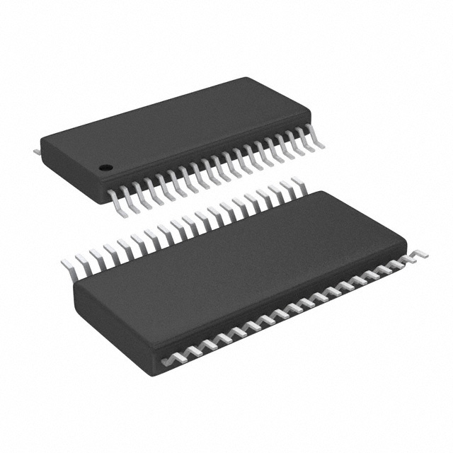


 工商网监
湘ICP备2023018690号
工商网监
湘ICP备2023018690号
